© 2016, IRJET | Impact Factor value: 4.45 | ISO 9001:2008 Certified Journal
| Page 183
Space Vector Modulation Strategy for NPC Converter
K.Murali Krishna Raju,
B.tech.,M.tech.,Guntur, Andhra Pradesh, India.
---***---Abstract
- A three-phase neutral point clamped (NPC)converter is presented for power factor correction and dc-link voltage regulation. A simplified space vector pulse width modulation scheme (SVPWM) is adopted to track line current commands. Using a simplified SVPWM algorithm, the calculate time for the time duration of voltage vector is reduced. The adopted NPC converter has less power switches compared with the conventional three-level NPC converter. Only eight power switches and four clamping diodes with voltage stress of half the dc bus voltage are used in the circuit configuration. Based on the proposed control algorithm, a reference voltage vector is generated on the ac terminal for drawing the sinusoidal line currents with unity power factor. Computer simulations are presented to verify the validity and effectiveness of the proposed control strategy.
1. Introduction
Power electronics are mainly deal with the efficient conversion, control and conditioning of electrical power by static means from its available input form into a desired electrical output form. The electrical power conversion can be realized by power converters built on power semiconductor switching devices and the converter are controlled by control electronics. This kind of power converter is usually known as switching mode converter.
Depending on power handling capabilities, the converters can be classified as
High power converters
Medium power converters and
Low power converters
As the power rating increases, to reduce the current rating of the converter, high voltage switching devices have to be used. High voltage switching devices are comparatively costlier and cannot be switched at high switching frequency. To overcome these problems, several new converter topologies have been used in high voltage applications. The circuit topologies of converters can be classified into [2]
Neutral point diode clamped (NPC) converters,
Flying capacitor clamped converters, and
Cascade full bridge converters.
Neutral point diode clamped and cascaded H-bridge converters are widely used for high power converter applications.
The number of levels in a converter bridge defines the number of voltage steps that are required by the converter bridge in order to achieve a certain voltage level at its output. Because power semiconductor switches have
limited voltage capability, the total voltage of a converter bridge is divided into a number of voltage steps, such that each voltage step can be handled by one power switch. Depending on voltage levels of converters can be classified as:
Two level converters and
Multilevel converters
The converters with voltage level three (or) more are referred as multilevel converters. Multilevel converters have been receiving increased attention recently, due to its capability of medium-voltage and high-power applications. The advantages of multilevel converters are low voltage rating of power semiconductors, low voltage harmonics and less electromagnetic interference.
Conventional diode rectifiers and thyristor rectifiers have several drawbacks such as large current harmonics, low power factor, and large power rating [1]. To overcome these problems, active current wave shaping techniques for single-phase and three-phase converters have been presented to improve the input power factor and draw the sinusoidal line currents form the ac mains. The sinusoidal pulse width modulation (SPWM) schemes have been widely used for the converter and inverter applications.
The advantages of SPWM for the converter application are drawing sinusoidal line currents with low harmonic contents, high power factor, dc link voltage regulation, and possible bidirectional power flow.
To compare with SPWM, space vector modulation (SVPWM) schemes have a lot of merits such as fast dynamic response, larger linear range of fundamental voltage, high dc link voltage utilization, low output voltage distortion, less total switching numbers of power switches, and less switching and conduction losses.
© 2016, IRJET | Impact Factor value: 4.45 | ISO 9001:2008 Certified Journal
| Page 184
2. Twelve Switch NPC Converter
The NPC converter is also called as diode clamped converter. It was first used in a three-level converter. Three-level NPC converter consists of three legs. Each leg contains four power switches and two clamping diodes. The two diodes clamp the switch voltage to half the level of the dc-bus voltages. Totally there are 27 switching combination are possible with this power switches. And three voltage levels are available in each leg. In three-level converter the dc-bus voltage is split into two series connected bulk capacitors. The middle point of the capacitors can be treated as neutral point. In conventional NPC converter each voltage level is generated on conduction and non-conduction functions of two legs.
Fig 2.1 shows the popular topology of diode-clamped (neutral-point diode-clamped) three-level converter. The circuit employs 12 power switching devices
[image:2.595.41.253.321.452.2]
Sa1S'c2
and six clamping diodes(Da1Dc2).Fig 2.1. Schematic Diagram of Three-Phase, Twelve Switch NPC Converter.
All the power semiconductor switches are assumed as ideal switches in the converter [3]. But in practical implementation IGBTs can be used as the switching devices. And the DC bus voltage is split into two series connected bulk capacitors, C1 and C2. The middle point of the two capacitors can be defined as the neutral point “O”. As the result of the diode clamped, the switch voltage is limited to half the level of the dc-bus voltageVd / 2. Thus, the voltage stress of switching devices
is greatly reduced. When switches S a' 1 and Sa2 are
turned-on, the converter input terminal A is connected to the neutral point through one of the clamping diodes.
The voltage Vao has three different
stagesVdc/2,0,Vdc/2similarly for leg B and C. Here takes leg A as an example. For voltage level Vdc/2, Sa1and Sa2
need to be turned on; for zero levelS'a1 and Sa2 need to
be turned on; and for Vdc/2, S'a1and S'a2need to be turned on. We can defined these states as +1, 0,-1 respectively. The switching stages of each bridge leg of three phase, three-level converter is described by using
switching variables F Fa, b andFc. In three- level converter, each bridge leg has three different switching stages.
3. Eight switch NPC converter
In eight-switch NPC converter consists of only two legs instead of three legs as in conventional NPC converter. In these two legs the construction of switches is similar to conventional NPC converter. The idea behind eight-switch NPC converter is to get the same dc bus voltage like three leg NPC converter, by minimum usage of switches. SVPWM is technique is used to get pulses for eight switch NPC converter.
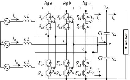
Fig 3.1 gives a circuit configuration of the adopted three-phase NPC converter. Two NPC legs are used in the converter. Each NPC leg has four power semiconductor switches and two clamping diodes. Each power semiconductor has a voltage rating of half the dc bus voltage. Three boost inductors are connected to converter on the ac terminal. These inductors are used to achieve boost operation and to achieve line current filtering. The phase C is directly connected to the midpoint of the split dc capacitors.
Fig 3.1 Schematic Diagram of Three-Phase, Eight Switch NPC Converter
Three valid voltage levels are generated on the ac terminal voltages VacandVbc. Five voltage levels are generated on the voltageVabbased on the proper operation of two NPC legs. The simplified space vector modulation is adopted to obtain the time duration of the selected voltage vectors. The time intervals of power switches corresponding to the selected voltage vectors are calculated to drive the converter. The control goals of the eight switch converter are to obtain a constant dc-link voltage. Balanced three-phase three-line ac source is used in the adopted system. The sum of the instantaneous three-phase voltages and currents is zero
0
xsaxsbxsc … (3.1)
Where x can be phase voltage (or) line current. The three-phase voltages and currents in the steady state are expressed as
cos( )
cos( 2 /3)
os( 2 /3)
vsa Vsm wt vsb Vsm wt vsc Vsmc wt
[image:2.595.309.539.373.485.2]© 2016, IRJET | Impact Factor value: 4.45 | ISO 9001:2008 Certified Journal
| Page 185
cos( ) cos( 2 /3)
os( 2 /3)
isa Ism wt
isb Ism wt
i I c wt
sc sm … (3.3)
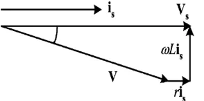
[image:3.595.41.188.289.362.2]Where Vsmand Ismare the peak voltage and peak current of three-phase ac source respectively, is the phase angle between the source voltage and line current. For a unity power factor operation, the phase angle between the line current and phase voltage is zero. Fig 3.2 shows the phasor diagram of the converter for unity power factor operation. For the rectifier operation, the line current is in phase with phase voltage. There is a phase lag between the source voltage Vs and reference control voltageV.
Fig 3.2 Phasor Diagram of the Converter for Unity Power Factor Operation
From the voltage equations on the ac terminal of the converter as shown in Fig 3.1, we have
isa vsa risa vaN d
L isb vsb risb vbN dt i v ri v
sc sc sc cN
… (3.4)
The differential Eqn. (3.4) can be rewritten in the orthogonal coordinate and expressed as
dIs
L Vs rIs V
dt … (3.5) dIs
V Vs rIs L dt
… (3.6) Where Vis the reference control Voltage.
Vsis the source voltage and
Isis the source current
If the voltage drop on the resistor “r” can be neglected, then the reference control voltage on the ac terminal in the synchronous reference frame is expressed as
,
disd
vd vsd L is q
dt
… (3.7)
,
disq
vq vsq L is d
dt
… (3.8)
Where
, vsd vs
T vsq vs
isd is T isq is
… (3.9)
, v vs sa
C v vs sb
vsc , i is sa
C i is sb
isc
1 1/ 2 1/ 2
2
3 0 3 / 2 3 / 2
C
…(3.10)
Using the coordinate transformation from the synchronous reference frame into the stationary reference
frame, the voltage commands Vand V are achieved.
VAnd Vare the projections of reference control voltages in stationary reference frame. Vand Vcan be expressed as
1v v d
T v v q
, Where
cos sin
sin cos
T
… (3.11)
The magnitude and phase angle of the reference control voltage V can be calculated as
2 2
V v v , tan 1 v v
(3.12)
4. SVPWM Technique for Eight Switch NPC
Converter:
Space vector modulation strategy is used for development of pulses of the eight switch NPC converter .For the adopted three-phase NPC converter, eight power switches, and four clamping diodes are used. The power switches Sxy and S'xy (x = a, b; y = 1, 2) are complementary to each other to avoid the short circuit in each converter leg. Three valid switching states are available in each converter leg to achieve three voltage levels vdc/2,0,vdc/2 on the ac terminal. For example of converter leg A, the upper two power switchesSa1andSa2are closed to achieve voltagevaovacvdc/2. In this operation state, line current isa is decreasing becausevsacvsavscvdc/2. If the power switches S'a1 andS'a2 are closed to turn on, the ac side voltagev v /2
ac dc . For this operation state, line current isa is increasing becausevsacvsavscvdc/2. A zero voltage level is generated on the voltage vac if the middle two switches
'1
Sa and Sa2 are closed. For this operation condition, the phase current i
sa is increasing (or decreasing) if the line voltage vsacis positive (or negative). Based on the above descriptions of three operation states in each converter leg, there are nine possible switching combinations in the adopted converter to control the line currents. The voltages measured on the ac terminals depend on the states of power switches and can be expressed as
2
2 vdc vaN vao voN fa voN
vdc vbN vbo voN fb voN
vcN voN
… (4.1)© 2016, IRJET | Impact Factor value: 4.45 | ISO 9001:2008 Certified Journal
| Page 186
1
0
1
1
0
1
Fa
Fb
if
if
if
if
if
if 1
'1
'1
1
'1
' 1 S a
Sa
Sa
Sb
Sb
S b and
and
and
and
and
and 2
2
' 2
2
2
' 2 S a
Sa
Sa
Sb
Sb
S b
are closed
are closed
are closed
are closed
are closed
are closed
… (4.2)
Based on the combinations of the switching states of switches, there are nine valid voltage vectors. The switching combinations can be represented by the order sets[Sa1,Sa2,Sb1,Sb2], whereSa11 denotes that power switch
1
Sa is closed, andSa10 denotes that power switch Sa1 is open. The same notation applied to power switches
,
2 1
Sa Sb andSb2. The reference control voltages vand vin the orthogonal coordinate can be obtained from the ac terminal voltages vacand vbcin the abccoordinate system by applying Eqn. (4.3) and These voltage vectors are given in Table 4.1
1
, 2 6
fb v fa vdc
1 2 2
v f v
b dc
[image:4.595.38.224.105.210.2] … (4.3)
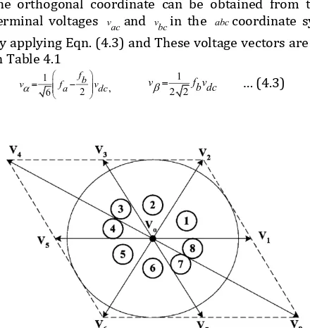
Fig 4.1 Space Vectors and Sectors in the Plan
[image:4.595.309.562.155.365.2]Fig. 4.1 gives the nine switching combinations and the corresponding voltage vectors in the orthogonal coordinate. There is one zero voltage vector (V0), six small voltage vectors (V1, V2, V3, V5, V6, V7), and two large voltage vectors (V4 and V8). The vectors V1 and V5, V2 and V6, V3 and V7 are opposite in direction. The small voltage vectors have a length of vdc/ 6 on the orthogonal coordinate plane. The other two vectors V4 and V8 are opposite in direction, but their vector length isvdc/ 2. These nine voltage vectors divide the whole circle into four sectors (sectors 1, 2, 5, and 6) with 600angle duration and four sectors (sectors 3, 4, 7 and 8) with 300angle duration. Fig. 4.1 and Table 4.2 show the definition of these sectors.
Table 4.1 Voltage Vectors in Different Switching Combinations
4.1 Synthesis Of The Reference Control Vector:
Based on the nine possible voltage vectors generated by the converter, there are eight sectors in the
,
coordinate system. The reference control voltage vector V* can be synthesized within one cycle time of length T. Based on the space vector technique, the reference control voltage vector V*can be expressed by two adjacent voltage vectors
* Tx Ty V Vx Vy
T T
… (4.3)
Where TxandTy are time duration of voltage vectors
Vxand Vy respectively, in each sector. The time durations
TxandTy have the following condition
Tx Ty To T … (4.4)
Where T0is time duration of voltage vectorV0 .
[image:4.595.42.262.310.543.2]© 2016, IRJET | Impact Factor value: 4.45 | ISO 9001:2008 Certified Journal
| Page 187
Table 4.2 Voltage Sectors and Adjacent Voltage Vectors
For example, three voltage vectors V1, V2, and V0 are used to compose reference voltage vector V*in the sector 1 (00–600).
The reference voltage vector V*is synthesized by
* 1 2 1 2
T T
V V V
T T
… (4.5)
By projecting the control voltage vector and two adjacent vectors onto the real and imaginary parts in the coordinate system, one can obtain the following relations
* 1 2
6 2 6
* 2
2 2
Vdc T Vdc T v
T T
Vdc T v
T
… (4.6)
The time durations of the selected switching vectors V V1 2, and V0 are easily calculated and expressed
as
Sector 1:
6 * 2 *
1
2 2 *
2
0 1 2
T v T v T
v v
dc dc
T v T vdc
T T T T
… (4.7)
The time duration of power switches Sa1,Sa2,Sb1andSb2are given by
; ; ;
1 1 2 2 1 2 2
TSa T T TSa T TSb T TSb T … (4.8)
The adjacent vectors in the other seven sectors are given in Table 4.2.
According to Eqn. 4.8 the reference voltage vector *
V can be composed to control the line currents with unity power factor. In the conventional space vector modulation, the magnitude and phase angle of the
reference voltage vector must be given to determine the sector location and to calculate the time duration of adjacent vectors. This control algorithm is so complicated that it requires a long computation time. To reduce the computation time of trigonometric function and square root operation in Eqn. (3.12), four lines are defined to divide the whole circle into eight sectors. These four lines are
0 1:
3 2:
3: 3
4: / 3 y P
y x P
P y x P
y x
… (4.9)
Therefore, any point of reference voltage vector *
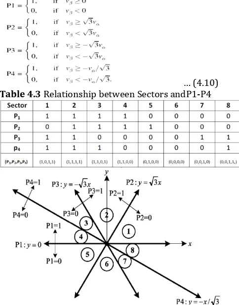
V in the orthogonal coordinate system can determine its location through these four equations in Eqn. (4.9). Table 4.3 and Fig. 4.2 give the relationships between the sector where the reference voltage vector V*lies in and the values of variables P1–P4. Variables P1–P4 are defined as
[image:5.595.309.551.331.640.2]… (4.10) Table 4.3 Relationship between Sectors andP1-P4
Fig 4.2 Relationships between Sector Where Reference Vector Lies and P1-P4
Now we can use variables P1–P4 to determine the sector where reference vector V* lies in and to calculate the time duration of power switches. No calculation of trigonometric function and square root operation is needed in the adopted algorithm.
© 2016, IRJET | Impact Factor value: 4.45 | ISO 9001:2008 Certified Journal
| Page 188
[image:6.595.46.410.86.597.2]in the synchronous reference frame is used in the control scheme.
[image:6.595.304.547.89.379.2]Fig 4.3 Block Diagram of the Adopted Control Algorithm
[image:6.595.39.281.244.597.2]Fig. 4.4. Simulated results of
3
voltages, values of variables P1–P4, and switching signals of power switches Sa1–Sb2.Fig. 4.5
. Simulated results. (a) Three-phase voltages
and currents.(b) Phase voltage v
saand ac terminal
voltages.
Fig. 4.6
. Simulated results of capacitor voltages on dc
terminal.
5. SIMULATION RESULTS
Some simulation results are presented to confirm the validity and effectiveness of the proposed control scheme. Simulation was performed in the SIMULINK toolbox of MATLAB. The power stage parameters of the three-phase converter are
[image:6.595.310.551.454.619.2]© 2016, IRJET | Impact Factor value: 4.45 | ISO 9001:2008 Certified Journal
| Page 189
3) boost inductor: 5 mH, 4) switching frequency: 20 kHz.
The line voltage is 110 V and source frequency is 50 Hz. The dc link voltage equals 400 V. Fig. 4.4 gives the simulation results of three-phase voltages, the values of four variables P1–P4 and the switching signals of power switches Sa1- S’b2. The sector of the reference voltage is decided from the values of P1–P4. In sector 1 of the voltage vector V*, the value of (P1,P2,P3,P4) equals (1,0,1,1). Fig. 4.5(a) shows the simulated waveforms of three-phase source voltages and currents. The line currents are sinusoidal waveforms with nearly unity power factor. The simulated waveforms of the phase voltage vsa and ac terminal voltages are given in Fig. 4.5(b). Three voltage levels are generated on the voltages vac and vbc, and five voltage levels are generated on the voltage vab. The simulated capacitor voltages on the dc terminal are illustrated in Fig.4.6. The ripple voltage on the capacitor is about 6 V.
6. CONCLUSION
A simple scheme based on space vector modulation for an eight-switch three-phase NPC converter is presented to save the calculation time, to obtain the time duration of power switches, and to control the line currents with unity input power factor. The circuit configuration is simple compared with the conventional twelve-switch three-phase NPC converter. Only eight power switches and four clamping diodes are used in the converter. In the proposed converter, the dc bus voltage is greater than two times of line voltage (vdc > 2vline). The size of capacitor in the proposed converter is twice larger than that in the conventional twelve switches NPC converter to maintain the same voltage ripple. With the proposed control scheme, the sinusoidal line currents with unity power factor drawn from the ac source and constant dc-link voltage are achieved. Computer simulation results are presented to demonstrate the validity and effectiveness of the proposed control scheme.
7. REFERENCES
[1] Bor-ren lin, and Ta-chang wei, “Space Vector Modulation Strategy for an Eight-Switch Three-Phase NPC Converter” IEEE Transactions on Aerospace and Electronic Systems Vol.40, No.2, 2004, pp.553-566.
[2] Bor-Ren Lin, Chun-Hao Huang and Ta-Chang Wei “Three-phase Neutral Point Clamped Converter Based on Space Vector PWM” IEEE Fifth International Conference on Power Electronics and Drive Systems, Vol.2,No.2, Nov. 2003, pp1369-1374.
K.Murali Krishna Raju Received The B.Tech. Degree In Electrical And Electronic Engineering From The JNTU Hyderabad, Andhra Pradesh, India. In 2003-07,
He Recived The M.Tech In Electrical Engineering From The JNTU Anantapur, Andhra Pradesh, India In 2007-2009.
From 2009 to 2010, he was worked as Assistant Professor in EEE department of “KRISHNA CHAITANYA INSTITUTE OF TECHNOLOGY AND SCIENCES”, MARKAPUR. He is currently working as Assistant Professor in EEE department of “CHALAPATHI INSTITUTE OF ENGINEERING AND TECHNOLOGY”, LAM, GUNTUR, from 2010.


