Temperature Variation Insensitive
Energy-Efficient CMOS
Circuits design in 65 nm Technology
SALENDRA.GOVINDARAJULU*1, DR. T.JAYACHANDRA PRASAD2,
1
Associate Professor, Department of E.C.E, RGMCET, Nandyal, JNTU, A.P-INDIA, 2
Principal, RGMCET, JNTU,A.P-INDIA,
*Corresponding AuthorE-mail address: [email protected]
Abstract
Operating an integrated circuit at the prescribed nominal supply voltage is not preferable for reliable circuit
operation under temperature fluctuations. In this work a design methodology based on optimizing the supply voltage for temperature variation insensitive circuit performance is proposed. Circuits display temperature variation insensitive delay, power, power delay product (PDP) characteristics when operated at a supply voltage 40% to 55% lower than the nominal supply voltage (VDD =1.0V) in a 65nm Deep Sub Micron (DSM) CMOS technology. The proposed design methodology of optimizing the supply voltage for temperature variation insensitive circuit performance is therefore, particularly attractive in low power applications with relaxed speed requirements. A new circuit technique is proposed in this work for simultaneously reducing the sub threshold &gate oxide leakage power in domino logic circuits.
Key words: Delay,Domino logic,Power, Power delay product, Supply voltage optimization, reliability
I.Introduction
for temperature variation insensitive circuit performance is, therefore, particularly attractive in low power applications with relaxed speed requirements. In this paper, the supply voltages that achieve minimum power-delay product at twodifferent temperatures are identified for circuits in 65nm CMOS technology. The power, delay, and power-delay product (PDP) are compared at the supply voltages that yield temperature variation insensitive circuit performance. Effect of temperature fluctuations on the device and circuit characteristics in 65nm CMOS technology is examined in Section IV. The optimum supply voltages for temperature variation insensitive circuit performance are presented in Section V. Simulation Results are discussed in Section VI. The tradeoffs of operating the circuits at the supply voltages providing temperature variation insensitive circuit speed are discussed in Section VII. Finally, conclusions are given in Section VIII.
II. Factors InfluencingMOSFETDrain Current Under Temperature Fluctuations
Device parameters that are affected by temperature fluctuations, causing variations in drain current produced by a MOSFET, are identified in this section. BSIM4 MOSFET current equations are used for an accurate characterization of drain current in deeply scaled nanometer devices. The drain current of a MOSFET is
0 r bulk dseff dseff gsteff
dseff sat eff
Weff A V V
Ids0= µeff V (1- )
V
Leff TOXE (2Vgsteff+4.vt) (1+ )
L
where Ids, Ids0,Vdseff, Vgsteff , Abulk, μeff ,Weff and Leff are the drain current with short-channel effects, drain current of a
long channel device, effective drain-to-source voltage, effective gate overdrive (VGS-Vt), parameter to model the bulk charge effect, effective carrier mobility, effective channel width and effective channel length, respectively. Threshold voltage, carrier mobility are
s s
( ) .
1 2
VthVTHO K Vbs K Vbs VtSCE Vt NULD VtDIBL
eff
gsteff fb s
bseff U0
µ = EU (3)
V +2(VTH0-V - )
1+(UA+UC.V )( )
TOXE
where Vth,VTHO,K1,K2,Vbs,∆VtSCE,∆VtNULD, ∆VtDIBL,μef,, UO, UA, UC, VTHO, Vfb, Φs, TOXE, &EU are the threshold voltage,
long channel threshold voltage at vbs=0, first order body bias coefficient, second order body bias co-efficient,bulk source voltage,short channel effect on vt,non-uniform lateral doping effect,drain induced barrier lowering effect of short channel on vt,effective mobility,low field mobility,co-efficient of first order mobility degradation due to vertical field, co-efficient of mobility degradation due to body bias effect, long channel threshold voltage at vbs=0v,flatbandvoltage,surface potential, oxide thickness, and coefficient.
III. Circuit Techniques
1. Static AND2, OR2, NAND2, NOR2, XOR2 2. Domino AND2, OR2, NAND2, NOR2, XOR2
Static AND2:
Fig.1. Block diagram of static AND2
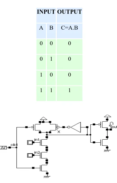
input to the AND gate is HIGH, a LOW output results. In another sense, the function of AND effectively finds the minimum between two binary digits, just as the OR function finds the maximum. The AND gate with inputs A and B and output C implements the logical expression C=A.B.
Table 1. Truth table
Domino AND2:
Fig:2. Block diagram of Domino AND2
Domino logic is attractive for high-speed circuits & it is 1.5 – 2x faster than static CMOS, so widely used in high-performance microprocessors. But many challenges: Monotonicity, Leakage, Charge sharing, Noise. The Fig.2 above shows X is a dynamic node holding value as charge on the node & eventually sub-threshold leakage charge may disturb to reduce the charge leakage by using keeper circuit and foot transistor is used to increase the performance of the circuit.
IV. Device and Circuit Behaviour Under Temperature Fluctuations
Influence of temperature fluctuations on device and circuit characteristics is evaluated in this section for 65nm CMOS technology. For circuits operating at the nominal supply voltage (VDD =1.0V in 65nm ), variations in gate overdrive are smaller as compared to carrier mobility variations when the temperature is increased from 27°C to107°C. The MOSFET drain current and the circuit speed are, therefore, reduced following the degradation of carrier mobility as the temperature is increased. Propagation power, delay, PDP variations ofvarious circuits with temperature at the nominal supply voltage are shown in Fig.3,4,5.
V. Supply Voltage Optimization
The results presented in Section IV indicate that operating an integrated circuit at the prescribed nominal supply voltage is not preferable for reliable circuit operation under temperature fluctuations. A design methodology based on scaling the supply voltage for suppressing the drain current variations due to temperature fluctuations is
INPUT OUTPUT
A B C=A.B
0 0 0
0 1 0
1 0 0
described in [2], [5], and [7]. In order to compensate for the variation of carrier mobility, the sensitivity of gate overdrive to temperature fluctuations should be enhanced by lowering the supply voltage [2]. At the optimum supply voltage, the temperature fluctuation induced gate overdrive variation completely counterbalances the carrier mobility variation [2]. The optimum supply voltages for various test circuits in a 65nm CMOS technology are presented in Fig.6,7,8. Circuits display a temperature variation insensitive performance when operated at a supply voltage 45% to 55% lower than the nominal supply voltage (VDD = 1.0V).
VI. Simulation Results
Fig.3. Percent Power variation with temperature for circuits operating at the nominal supply voltage (VDD = 1.0V) in a 65nm CMOS technology.
Fig.4. Percent Delay variation with temperature for circuits operating at the nominal supply voltage (VDD = 1.0V) in a 65nm CMOS technology.
Fig.5. Percent PDP variation with temperature for circuits operating at the nominal supply voltage (VDD = 1.0V) in a 65nm CMOS technology.
17.2%
9.8% 37.6% 12.8% 46.7% 17.6% 9.1% 11.3% 2.1% 2.9%
Percent Power Variation when the Temperature is increased from 27 0 C to 107 0 C
0 1 2 3 4 5
Static
AND2 DominoAND2 StaticOR2 DominoOR2 NAND2StaticDominoNAND2 NOR2StaticDominoNOR2 XOR2StaticDominoXOR2 Circuits in a 65nm Technology
27 Degrees 107 Degrees
Power
(
µ
W
)
3.8%
2.4%
1.6% 0.6% 1.2% 1.1% 0.3% 2.5% 4.3% 1.6%
Percent PDP Variation when the Temperature is increased from 27 0 C to 107 0 C
0 1 2 3 4 5
Static
AND2 DominoAND2 StaticOR2 DominoOR2 NAND2StaticDomino NAND2NOR2StaticDominoNOR2 XOR2StaticDominoXOR2 Circuits in a 65nm Technology
PDP
( 1
0
-1
8)
27 Degrees 107 Degrees 2.2%
1.1% 0.9% 0.9% 0.8% 0.4% 0.7% 0.6% 0.8%
0.2%
Percent Delay Variation when Temperature is increased from 27 0 C to 107 0 C
0.12 0.10 0.06 0.04 0.0
0.06
0.04
0.02
0.00
Static AND2
Domino AND2
Static OR2
Domino OR2
Static NAND2
Domino NAND2
Static NOR2
Domino NOR2
Static XOR2
Domino XOR2 Circuits in a 65nm CMOS Technology
Del
ay ( n s )
Fig.6. Optimum supply voltages that achieve temperature variation insensitive power characteristics in a 65nm CMOS technology.
Fig.7. Optimum supply voltages that achieve temperature variation insensitive delay characteristics in a 65nm CMOS technology.
Fig.8. Optimum supply voltages that achieve temperature variation insensitive
PDP characteristics in a 65nm CMOS technology 6.6%
1.1%
0.1% 1.6% 1.5%
2.6% 0.8% 2.2% 1.0% 2.9%
Optimum Supply Voltages for Temperature Variation insensitive Circuit performance
0 0.2 0.4 0.6 0.81 1.2 1.4 1.6
Static AND2
Domino AND2
Static OR2
Domino OR2
Static NAND2
Domino NAND2
Static NOR2
Domino NOR2
Static XOR2
Domino XOR2
Circuits in a 65nm Technology
P
owe
r
(
µ
W
)
27 Degree 107Degree
0.7%
0.7%
0.2% 0.5% 0.1% 0% 0% 0% 0.2% 0%
Optimum supply Voltages for Temperature Variation insensitive Circuit Performance
Static
AND2 DominoAND2 StaticOR2 DominoOR2 NAND2StaticNAND2DominoNOR2StaticDominoNOR2 XOR2StaticDominoXOR2 Circuits in a 65nm CMOS Technology
PDP
( 1
0
-1
8 )
27 Degrees 107 Degrees 0.07
0.06 0.05 0 0.05
0.04
0.02
0.2%
0.3% 0.2% 0% 0.4% 0% 0% 0.1% 0.1% 0.1%
Optimum Supply Voltage for Temperature variation insensitive Circuit Performance
0 0.05 0.1 0.15 0.2 0.25 0.3
Static
AND2 DominoAND2 StaticOR2 DominoOR2 NAND2StaticDominoNAND2NOR2StaticDominoNOR2 XOR2StaticDominoXOR2 Circuits in 65nm CMOS Technology
Del
ay ( n s )
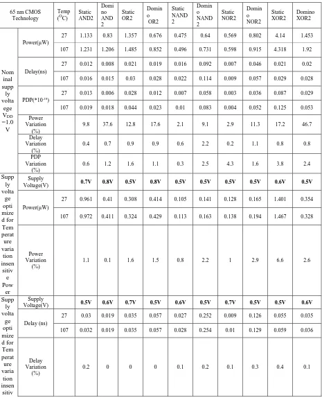
Table 2.
NORMALIZED POWER, DELAY, POWER-DELAY PRODUCT AND DELAY VARIATIONS AT THE NOMINAL SUPPLY VOLTAGE, SUPPLY VOLTAGE OPTIMIZED FOR TEMPERATURE VARIATION INSENSITIVE POWER, DELAY, PDP IN A 65
nm CMOS TECHNOLOGY
65 nm CMOS Technology
Temp (OC)
Static AND2 Domi no AND 2 Static OR2 Domin o OR2 Static NAND 2 Domin o NAND 2 Static NOR2 Domin o NOR2 Static XOR2 Domino XOR2 Nom inal supp ly volta ege VDD =1.0 V Power(µW)
27 1.133 0.83 1.357 0.676 0.475 0.64 0.569 0.802 4.14 1.453
107 1.231 1.206 1.485 0.852 0.496 0.731 0.598 0.915 4.318 1.92
Delay(ns)
27 0.012 0.008 0.021 0.019 0.016 0.092 0.007 0.046 0.021 0.02
107 0.016 0.015 0.03 0.028 0.022 0.114 0.009 0.057 0.029 0.028
PDP(*10-18)
27 0.013 0.006 0.028 0.012 0.007 0.058 0.003 0.036 0.087 0.029
107 0.019 0.018 0.044 0.023 0.01 0.083 0.004 0.052 0.125 0.053
Power Variation
(%)
9.8 37.6 12.8 17.6 2.1 9.1 2.9 11.3 17.2 46.7
Delay Variation
(%)
0.4 0.7 0.9 0.9 0.6 2.2 0.2 1.1 0.8 0.8
PDP Variation
(%)
0.6 1.2 1.6 1.1 0.3 2.5 4.3 1.6 3.8 2.4
Supp ly volta ge opti mize d for Tem perat ure varia tion insen sitiv e Pow er Supply
Voltage(V) 0.7V 0.8V 0.5V 0.8V 0.5V 0.5V 0.5V 0.5V 0.6V 0.5V
Power(µW)
27 0.961 0.41 0.308 0.414 0.105 0.141 0.128 0.165 1.401 0.354
107 0.972 0.411 0.324 0.429 0.113 0.163 0.138 0.194 1.467 0.328
Power Variation
(%)
1.1 0.1 1.6 1.5 0.8 2.2 1 2.9 6.6 2.6
Supp ly volta ge opti mize d for Tem perat ure varia tion insen sitiv Supply
Voltage(V) 0.5V 0.6V 0.7V 0.5V 0.6V 0.5V 0.7V 0.5V 0.5V 0.6V
Delay (ns)
27 0.03 0.019 0.035 0.057 0.027 0.252 0.009 0.126 0.055 0.035
107 0.032 0.019 0.035 0.057 0.028 0.254 0.01 0.129 0.059 0.036
Delay Variation
(%)
e Dela
y Supp
ly volta
ge opti mize d for Tem perat ure varia tion insen sitiv
e PDP
Supply
Voltage(V) 0.5V
0.65
V 0.7V 0.5V 0.65V 0.5V 0.7V 0.5V 0.5V 0.6V
PDP(*10-18)
27 0.007 0.004 0.021 0.008 0.004 0.053 0.002 0.02 0.052 0.016
107 0.008 0.004 0.023 0.008 0.004 0.06 0.002 0.025 0.059 0.018
PDP Variation
(%)
0.1 0 0.2 0 0 0.7 0 0.5 0.7 0.2
VII. Temperature Variation Insensitive Low Power CMOS Circuits
The tradeoffs of operating the circuits at the supply voltages providing temperature variation insensitive circuit performance are discussed in this section. The power, delay, and power-delay product (PDP) at the supply voltages that yield temperature variation insensitive circuit performance are compared.
At the supply voltages for minimum power-delay product, the power per cycle is 32% to 96% lower than the energy per cycle at the nominal supply voltage (VDD = 1.0V). Similarly, the power per cycle at the optimum supply voltages that yield temperature variation insensitive circuit performance is 37% to 79% lower than the power per cycle at the nominal supply voltage. The circuit speed, as compared to the speed at the nominal supply voltage, degrades by upto 1.8% to 16% when the circuits are operated at the supply voltages for minimum power-delay product (VDD optimized for minimum PDP at 107°C) and temperature variation insensitive circuit performance, respectively.
The power-delay product at the optimum supply voltages that yield temperature variation insensitive circuit performance is 6.6% to 50% lower than the power-delay product at the nominal supply voltage. Low-power integrated circuits can, therefore, also be made insensitive to temperature fluctuations with a modest amount of increase in power-delay product. Optimum supply voltage for temperature variation insensitive low power circuits is, therefore, feasible.
VIII. Conclusions
A design methodology for temperature variation insensitive low power circuits in a 65nm CMOS technology is presented in this paper. When operating at the nominal supply voltage, the speed of circuits degrade by up to 2.2% and the power PDP of the circuits degrade by up to 46.7% & 4.3% as the temperature is increased from 27°C to 107°C. Operating an integrated circuit at the prescribed nominal supply voltage is not preferable for reliable circuit operation under temperature fluctuations. Circuits display a temperature variation insensitive performance when operated at a supply voltage 40% to 55% lower than the nominal supply voltage (VDD = 1.0V). Integrated circuits operating at scaled supply voltages consume low power at the cost of reduced performance. The design methodology of optimizing the supply voltage for temperature variation insensitive circuit performance is, therefore, particularly attractive in low power applications with relaxed speed requirements.
References
[1] S. Borkar, T. Karnik, S. Narendra, J. Tschanz, A. Keshavarzi and V. De, “Parameter Variation and Impact on Circuits and Micro architecture,” Proceedings of the IEEE/ACMInternational Design Automation Conference, pp. 338-342,June 2003.
[2] R. Kumar and V. Kursun, “Voltage Optimization For Temperature Variation Insensitive CMOS Circuits,”Proceedings of the IEE
International Midwest Symposium onCircuits and Systems, pp. 476-479, August 2005.
[3] Y. Cheng, K. Imai, M. C. Jeng, Z. Liu, K. Chen, and C. Hu,“Modeling Temperature Effects of Quarter MicrometreMOSFET in BSIM3v3 for Circuit Simulation,” SemiconductorScience Technology, Vol. 12, pp. 1349-1354, November 1997.
[4] Y. P. Tsividis, Operation and Modeling of the MOS Transistor,McGraw-Hill, New York, 1999.
[5] A. Bellaouar, A. Fridi, M. J. Elmasry, and K. Itoh, “Supply Voltage Scaling for Temperature Insensitive CMOS Circuit Operation,” IEEE
Transactions on Circuits and Systems II, Vol.45, No. 3, pp. 415-417, March 1998.
[6] R. W. Johnson et al., “The Changing Automotive Environment: High Temperature Electronics,” IEEE Transactions onElectronics Packaging Manufacturing, Vol. 27, No. 3, pp. 164-176, July 2004.
[7] I.M. Filanovsky and A. Allam, “Mutual Compensation of Mobility and Threshold Voltage Temperature Effects with Applications in CMOS Circuits,” IEEE Transactions onCircuits and Systems I, Vol. 48, No. 7, pp. 876-884, July 2001.
[8] S.Govindarajulu, T.Jayachandra Prasad, “Low power,Energy-efficient Domino Logic Circuits”, IJRTE, vol.2, No.7, Nov.2009, pp.30-33, Academy Publishers, ACEEE, Finland.
[9] S.Govindarajulu, T.Jayachandra Prasad, “Low-Power, High Performance Dual Threshold Voltage CMOS Domino Logic Circuits”, published in ICRAES, 8th & 9th Jan’2010, pp-109-117,KSR College of Engg., Tiruchengode, India.
[10] S.Govindarajulu, T.Jayachandra Prasad, “Robust, Energy-efficient Reduced Swing Domino Logic Circuits”, IJRTE, vol.3, No.4, pp.129-133, May.2010, Academy Publishers, ACEEE, Finland, “in Press”
[11] S.Govindarajulu, T.Jayachandra Prasad, “Considerations of Performance Factors in CMOS Designs”, ICED 2008, Dec.1-3 ,Penang, Malaysia, IEEE Xplore.
[12] Google website.
Biographical Notes
1
Salendra.Govindarajulu:- He is working as an Associate Professor in the Dept. of Electronics & Communication Engg. at RGMCET, Nandyal, Andhra Pradesh, India. He presented more than 11 International/National Technical Papers. He is a Life Member of ISTE, New Delhi. His interest includes Low Power VLSI CMOS design.
2