UCL
D epartm ent of Electronic and Electrical Engineering
UNIVERSITY COLLEGE LONDON
TORRINGTON PLACE LONDON WCIE 7JE ENGLAND
Design of a Fully Tunable GaAs MESFET OTA-C Integrator
Suitable For High-Precision Continuous-Time Filtering
Pasqualino Michele Visocchi
Thesis subm itted to the U niversity o f London fo r the degree o f Doctor o f Philosophy
ProQuest Number: 10017764
All rights reserved
INFORMATION TO ALL USERS
The quality of this reproduction is dependent upon the quality of the copy submitted.
In the unlikely event that the author did not send a complete manuscript and there are missing pages, these will be noted. Also, if material had to be removed,
a note will indicate the deletion.
uest.
ProQuest 10017764
Published by ProQuest LLC(2016). Copyright of the Dissertation is held by the Author.
All rights reserved.
This work is protected against unauthorized copying under Title 17, United States Code. Microform Edition © ProQuest LLC.
ProQuest LLC
789 East Eisenhower Parkway P.O. Box 1346
Abstract
The O perational T ransconductance Amplifier-C (OTA-C) integrator has become the favoured building block for the im plem entation of integrated C ontinuous Time (CT) filters by m any researchers around the w orld. The use of an OTA-C integrator for the realisation of an integrated CT filter does how ever, require full tunability, since the integrator tim e constants are dependent on absolute fabricated com ponent values w hich are subject to process tolerances. In addition, the OTA m ay be used as a linear tunable resistor providing filter Q control. Integrated CT filters using OTA-C
integrators have been im plem ented in Si CMOS, bipolar and GaAs MESFET technologies, w ith dem onstrated operating frequencies ranging from 10s of KHz to 2GHz.
This thesis describes a novel circuit for the realisation of an OTA-C integrator to be u sed for the im plem entation of a bandpass CT filter. The new OTA-C integrator, which has been fabricated in 0.5pm GaAs MESFET technology, features independently tunable intrinsic o u tp u t conductance, and transconductance. Thus additional OTAs configured as extrinsic linear resistors to provide Q-control are not required. A novel m ethod of
Contents
Title Page
1
Abstract
2
Table of Contents
3
List of Figures & Tables
7
Dedication
14
Acknowledgements
15
Abbreviations
17
1. Introduction
21
1.1 Background 21
1.2 Overview of Thesis 23
1.3 Statement of Originality 24
2.1ntegrated Continuous Time Filters : A Review
26
2.1 Introduction 27
2.2 The State Variable Filter 27
2.3 Active Tunable Integrators 30
2.3.1 Voltage Amplifier (Op Amp) M ethod 30
2.3.2 Transconductance Am plifier M ethod 33
2.4 Higher Order Filters; Design Topologies 36
2.4.1 Cascade Approach 36
2.4.2 LC Ladder Prototype Approach 37
2.5 Integrators : Characteristics and Limitations 44
2.5.1 Ideal Integrator 44
2.5.2 Non Ideal (Practical) Integrator 45
2.5.3 Transconductance - Op Amp Integrator 52
2.6 Automatic Tuning 53
2.7 Review of Fabricated Continuous Time Filters 56
2.8 Conclusion 58
S.High Order Continuous Time Filters : Fundamental
Active Building Blocks and Their Limitations
60
3.1 Introduction 61
3.2 Realisation of a 12th order Bandpass Filter 61
3.2.1 M otivation for Active Filter Integration 61
3.2.2 Passive Prototype of a Transissional Gaussian to 6dB 63
3.2.3 Active Transissional Gaussian using 2nd order sections 66
3.3 Effects of non-ideal Transconductors on Transfer Function. 70
3.3.1 Am plitude Response 70
3.3.2 Group Delay Response 73
3.3.3 Effects on Control Parameters 75
3.4 Requirements of an Active 2nd order Tunable Filter 78
3.4.1 Frequency and Q tuning Range 78
3.4.2 Transfer Function Accuracy 80
3.5 Conclusion 83
4. GaAs MESFET Technology
85
4.1 Introduction 86
4.2 The Physics of Gallium Arsenide : a summary 86
4.3 M odelling : Problems & Restrictions 89
4.3.1 The GaAs MESFET 89
4.3.2 The DC Models 91
4.3.3 MESFET Geometry 94
4.4 Conclusions 103
5. A Novel OTA-C Integrator Approach Realised in
GaAs MESFET Technology
104
5.1 Introduction 105
5.2 Basic GaAs MESFET OTA 105
5.3 Bootstrap Gain Enhancement 107
5.3.1 Fixed Voltage Gain-Enhancement Techniques 107
5.3.2 The Variable Gain Bootstrap Method 111
5.3.3 Sensitivity and Tuning 113
5.4 A Novel Transconductance (Gm) Tuning Method 115
5.4.1 The AC Current Shunt Method 115
5.4.2 Tuning Range and Extension 118
5.5 Fully Balanced OTA and Load Conductance 121
5.5.1 Tunable OTA 121
5.5.2 Tunable Load Conductance 123
5.5.3 Common Mode Stability 124
5.6 Simulated Performance of OTA-C Integrator 125
5.6.1 Single-Ended OTA-C Integrator 125
5.6.2 Integrator Frequency Response w ith Tuning 127
5.6.3 Integrator Distortion w ith Tuning 130
5.7 Simulated Performance of Bandpass Filter 133
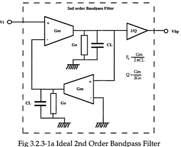
5.7.1 2nd order CT Bandpass Filter 133
5.7.2 Bandpass Filter Frequency Response w ith Tuning 134
5.7.3 Transfer Function Accuracy 136
5.8 Conclusion 139
6. Experimental Results of OTA-C Integrator
and Bandpass Filter
140
6.1 Introduction 141
6.2 Measured Performance of OTA-C Integrator 141
6.2.2 Experimental Evaluation Method 143
6.2.3 Integrator Frequency Response Measurements 150
6.2.4 Integrator Distortion Measurements 153
6.3 Measured Performance of Bandpass Filter 156
6.3.1 2nd Order CT Bandpass Filter 156
6.3.2 Experimental Evaluation M ethod 158
6.3.3 Bandpass Filter Frequency Response Measurements 163
6.3.4 Intermodulation Distortion Measurements (IMD) 165
6.3.5 Transfer Function Accuracy 166
6.4 Conclusion 173
7 Conclusions and Future Work
174
7.1 Conclusions of Thesis 174
7.2 Suggestions for Future Work 175
Published Papers
177
References
179
List Of Figures & Tables
Figures :
Chapter 2
Fig 2.2-1 Simple RLC Filter
Fig 2.2-2 SFG of RLC Filter (a) N odal Representation of Equation (2.2.3) (b) Equivalent
Fig 2.2-3 State-Variable voltage representation of an RLC Filter Prototype
Fig 2.2-4 State-Variable representation of an RLC Filter w ith Lossy Inductor
Fig 2.3.1-1 (a) Classical Active RC Integrator (b) SFG R epresentation Fig 2.3.1-2 (a) Small-signal active RC integrator w ith variable time
constant (b) E quivalent circuit elem ent replacem ent Fig 2.3.1-3 (a) Lossy Tunable Integrator (b) SFG R epresentation Fig 2.3.1-4 Active 2nd O rder Filter using the MOSFET-C approach Fig 2.3.2-1 Symbol for a Transconductance Am plifier
Fig 2.3.2-2 (a) Transconductance-C integrator (b) SFG Representation Fig 2.3.2-3 Simulating a gro u n d ed variable resistor w ith a Tunable
T ransconductor
Fig 2.3.2-4 (a) Lossy Tunable Transconductance-C Integrator (b) SFG R epresentation
Fig 2.3.2-S Active 2nd O rder Filter using the Transconductance-C approach
Fig 2.4.1-1 Cascade Realisation of an n^h O rder Transfer Function Fig 2.4.2-1 (a) Passive 2nd order Lowpass LC Prototype (b) Lowpass to
Bandpass T ransform ation (c) Passive 4th order Bandpass LC Prototype
Fig 2.4.2-2 (a) N odal Signals of 4th order Bandpass Filter (b) SFG R ep resen tatio n
Fig 2.4.2-3 (a) Minimised SFG of 4th order LC bandpass Filter (b) Active Realisation u sing Integrators
Fig 2.43-2 (a) G yrator Simulation of a (b) grounded Inductor Fig 2.4.3-S (a) G yrator Sim ulation of a (b) floating Inductor
Fig 2.4.3-4 G yrator Realisation using T ransconductance A m plifiers Fig 2.4.3-5 Transconductance-C Sim ulation of (a) grounded inductor
and (b) floating inductor
Fig 2.5.1-1 (a) Integrator A m plitude (b) Phase Response Fig 2.5.2-1 Practical (non-ideal) OTA-C integrator
Fig 2.S.2-2 (a) Practical Integrator A m plitude (b) Phase Response Fig 2.5.2-3 2nd o rd er Resonator realisation using practical
T ransconductance A m plifiers
Fig 2.5.3-1 Transconductance-C O p Am p Integrator
Fig 2.6-1 M aster - Slave A utom atic Tuning System Block D iagram
Chapter 3
Fig 3.2.1-1 Sim plified RF Front-end of SSR T ransponder
Fig 3.2.2-1 N orm alised Low-Pass Transitional G aussian to 6dB Fig 32.2-2 Passive Prototype of a 12th order Bandpass Transitional
G aussian to 6dB (Q of 6, Centre Frequency of 60MHz)
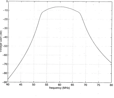
Fig 3.2.2-2a A m plitude Response of 12th ord er Transitional G aussian to 6dB
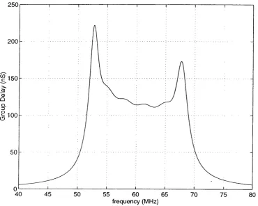
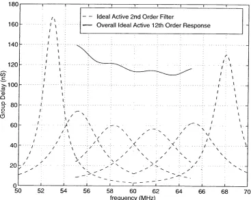
Fig 3.2.2-2b G roup Delay Response of 12th Transitional G aussian to 6dB Fig 3.2.3-la Ideal 2nd O rder Bandpass Filter
Fig 3.2.3-lb Cascaded 2nd O rder bandpass Filter to Realise 60MHz Bandpass Transitional G aussian to 6dB Response
Fig 3.2.3-2a A m plitude Response of each 2nd o rd er Filter and over all R esponse
Fig 3.2.3-2b G roup Delay Response of each 2nd order Filter and over all R esponse
Fig 3.3.1-1 N on-ideal 2nd order bandpass filter
Fig 3.3.1-2a N orm alised A m plitude Response of 60MHz Transitional G aussian Filter w ith non-ideal T ransconductance Am plifiers w ith Fu of infinity, 15GHz and lOGHz
Fig 3.3.2-la G roup Delay Ripple Response of 60MHz Transitional
G aussian Filter w ith non-ideal T ransconductance A m plifiers w ith Fu of infinity, 15GHz and lOGHz
Fig 3.3.2-lb G roup Delay Ripple Response of 60MHz Transitional
G aussian Filter w ith non-ideal T ransconductance A m plifiers w ith Fu of 5GHz, IG H z and 500MHz
Fig 3.3.3-1 Transconductance A m plifier DC Gain (G m /G o) w ith Finite U nity Gain B andw idth, Fu
Fig 3.3.3-2 Q Enhancem ent w ith Finite U nity Gain B andw idth, Fu
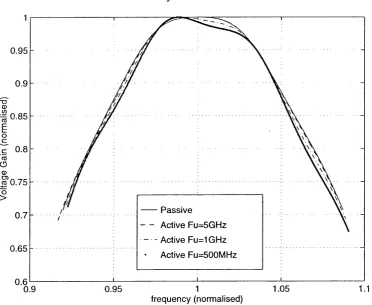
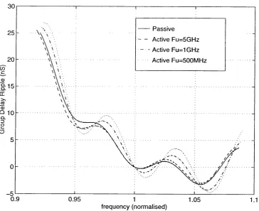
Fig 3.3.3-3a N orm alised A m plitude Response of the 12th O rder Bandpass Filter w ith Passive and Active Realisation w ith a Fu of 5GHz Fig 3.3.3-3b G roup Delay Ripple Response of the 12th O rder Bandpass
Filter w ith Passive and Active Realisation w ith a Fu of 5GHz Fig 3.4.2-la A m plitude Response of 2nd order Bandpass Filter w ith a Q of
30
Fig 3.4.2-lb G roup Delay Response of 2nd order Bandpass Filter w ith a Q of 30
Fig 3.4.2-2a Error in A m plitude Response C om pared to the Ideal Fig 3.4.2-2b Error in G roup Delay Response C om pared to the Ideal C hapter 4
Fig 4.2-1 Drift Velocity in Si and GaAs Fig 4.3.1-1 Schematic of a Typical D-MESFET
Fig 4.3.2-1 Shichman-Hodges M odel of FET Characteristics (P = ImA/V^, X = O.lV-1, Vto = -2V)
Fig 4.3.2-2 M easured Characteristic of the GEC-Marconi 20|im GaAs
MESFET w ith Shichm an-H odges and Curtice m odels
Fig 4.3.3-1 Sim ulated Id - V^g Characteristics for a 20)Lim MESFET
(Model Param eters derived from M easured Data) Fig 4.3.4-1 Small Signal M odel for the 20pm GaAs MESFET Fig 4.3.4-2a Sim ulated Small Signal Frequency Response of 20pm
MESFET C urrent G ain H21
C hapter 5
Fig 5.2-1 Basic MESFET T ransconductor Cell Fig 5.2-2 Single Cascode Am plifier Cell Fig 5.3.1-1 G eneralised Bootstrap Load
Fig 5.3.1-2 (a) Bootstrap Load (b) Im proved Bootstrap Load Fig 5.3.1-3 Self-Bootstrapped Load
Fig 5.3.2-1 Variable Bootstrapped Load Circuit Fig 4.3.2-2 C om plete Variable Bootstrap Load Fig 5.4.1-1 Variable Gain OTA
Fig 5.4.1-2 D ouble Cascode Variable G ain OTA Fig 5.4.2-1 C om plete Variable G ain OTA
Fig 5.4.2-2 Gm Frequency Response w ith Tuning
Fig 5.5.1-1 Fully Balanced, Differential OTA W ith Controllable T ransconductance, Gm
Fig 5.5.2-1 Fully Balanced, Variable Load Conductance, Go Fig 5.5.3-1 C om m on M ode Stabilization C ircuit
Fig 5.5.3-2 C om plete Duel Input Fully Balanced OTA-C Integrator
Fig 5.6.1-1 C om plete Fully Tunable OTA-C Integrator w ith Independent Control of Cm and Go
Fig. 5.6.2-la Single-Ended A m plitude & Phase Response of the OTA-C Integrator (Gm constant. Go varied)
Fig. 5.6.2-lb Single-Ended A m plitude & Phase Response of the OTA-C Integrator (Gm varied. Go constant)
Fig. 5.6.2-2a Fully Balanced A m plitude & Phase Response of the OTA-C Integrator (Gm constant. Go varied)
Fig. 5.6.2-2a Fully Balanced A m plitude & Phase Response of the OTA-C Integrator (Gm constant. Go varied)
Fig. 5.6.3-1 Resistive Load (1/G m ) and Voltage Gain (30dB) Frequency Response (Cp=0)
Fig 5.7.1-1 Fully Tunable 2nd O rder B andpass Section
Fig 5.7.2-la Q T uning Frequency Response (Gm constant : Go varied)
Fig 5 .7 3 -la A m plitude Response of 2nd order bandpass Filter Fig 5.7.3-lb G roup Delay Response of 2nd order bandpass Filter Fig 5.7.3-2a Error in A m plitude Response C om pared to the Ideal Fig 5.7.3-2b Error in G roup Delay Response C om pared to the Ideal C hapter 6
Fig 6.2.1-1 Com plete Fully Tunable OTA-C Integrator w ith In dependent Control of Gm and Go
Fig 6.2.1-2a Photom icrograph of OTA-C Chip
Fig 6.2.1-2b Pin Layout of Fabricated OTA-C Integrators Fig 6.2.2-la Purpose Build Test Board
Fig 6.2.2-lb On Board Bias Voltages and C om ponent Values
Fig 62.2-2 Photograph of Purpose Build Test Board w ith Test IC
Fig 6.2.2-3 M easurem ent A pparatus For OTA-C Integrator Evaluation Fig 6.2.2-4 (a) OTA-C Integrator w ith O u tp u t Buffer (b) Packaged O u tp u t
Buffer for Calibration
Fig 6.2.2-5a Frequency and Phase Response of Test Board and O u tp u t Buffer
Fig 6.2.2-5b Frequency and Phase Response after calibration of Test Board and O u tp u t Buffer
Fig 6.2.3-1 Gm M easurem ent, Frequency Response and T uning Range Fig 6.2.3-2a A m plitude Response of OTA-C Integrator (Gm constant. Go
varied)
Fig 6.2.3-2b A m plitude Response of OTA-C Integrator (Gm varied, G m /G o constant)
Fig 6.2.3-2b O u tp u t Spectrum of O u tp u t Buffer Subjected w ith an In p u t Signal of 1.2Vp-p
Fig 6.3.1-1 Fully Tunable 2nd O rder Bandpass Filter
Fig 6.3.1-2a Photom icrograph of the Fully Tunable 2nd O rder Bandpass Filter Chip
Fig 6.3.1-2b Pin Layout of Fabricated 2nd O rder Bandpass Filter Fig 6.3.2-1 Purpose Built Test Board
Fig 6.3.2-2 Photograph of Purpose Build Test Board w ith Test IC Fig 6.3.2-3 M easurem ent A pparatus For 2nd O rder Bandpass Filter
Fig 63.2-4 (a) Bandpass Filter w ith O utput Buffer (b) Packaged O u tp u t Buffer for C alibration
Fig 6.3.2-5a Frequency and Phase Response of Test Board and O u tp u t Buffer
Fig 6.3.2-5b Frequency and Phase Response after calibration of Test Board and O u tp u t Buffer
Fig 6.3.3-la A m plitude Response of 2nd O rder Bandpass Filter (Gm varied. Go constant)
Fig 6.3.3-lb A m plitude Response of 2nd O rder Bandpass Filter (Gm constant. Go varied)
Fig 6.3.4-1 (a) IMD M easurem ents w ith Fo constant, Q variable (b) IMD M easurem ents w ith Fo variable, Q constant
Fig 6.3.5-la A m plitude and Phase Response of 2nd O rder B andpass Filter (Fo=50MHz, Q=32)
Fig 6.3.5-lb A m plitude and Phase Response of 2nd O rder Bandpass Filter (Fo=12MHz, Q=29)
Fig 6.3.5-2a A m plitude Response of 2nd O rder Bandpass Filter and Ideal Response at 50MHz
Fig 6.3.5-2b A m plitude Response of 2nd O rder Bandpass Filter and Ideal Response at 12MHz
Fig 6.3.5-3a Error in A m plitude Response of 2nd O rder Bandpass Filter at 50MFIz
Fig 6.3.5-3b Error in A m plitude Response of 2nd O rder Bandpass Filter at 12MHz
Fig 6.3.5-4a Group Delay Response of 2nd O rder Bandpass Filter and Ideal Response at 50MHz
Fig 6.3.5-4b Group Delay Response of 2nd O rder Bandpass Filter and Ideal Response at 12MHz
Fig 6.3.5-5a Group Delay Response of 2nd O rder Bandpass Filter and Ideal Response w ith the passband at 50MHz
Tables :
C hapter 2 Table 2.5.2-1 Table 2.7-1
C hapter 3 Table 3.2.3-1
Effect of pole spacing on phase shift of Integrator Review of Fabricated CT Filters for H igh Frequency O peration
Required Q, Centre Frequency Fo, and Complexity FoQ, to realise the 60MHz IF Bandpass Filter
C hapter 4 Table 4.2-1 Table 4.3.3-la
Carrier Mobilities in Si and GaAs
M aximum V ariation of MFSFFT Param eters Across a Single W afer
Table 4.3.3-lb M aximum Variation of MFSFFT Param eters Across Four Foundry Runs
SPICF Param eters for the 20pm GaAs MFSFFT Table 4.3.4-1
C hapter 5 Table 5.6.3-1
Table S.6.3-2
Table S.6.3-3
C hapter 6 Table 6.2.4-1 Table 6.2.4-2
Total Harm onic D istortion of OTA Transconductance Gm (short circuit o utput current) : (a) Single-Fnded (b) Fully Balanced
Total H arm onic D istortion of OTA Voltage Gain (1 /G m Resistive Load) : (a) Single-Fnded (b) Fully Balanced
Total Harm onic D istortion of OTA Voltage Gain (Load O pen Circuit, Go) : (a) Single-Fnded (b) Fully Balanced
To m y G randm other M aria Cristina Bastianelli
1906 -1991
"He who stands a lo o f runs the risk o f believing h im self better than others and m isusing his critique
o f society as an ideology fo r his private interest. W hile he gropingly fo rm s his own life in the fra il image o f true existence, he should never fo rg et its fra ilty , nor how little the image is a substitute fo r
true life."
Acknowledgment
There is no d o ubt in m y m ind th at this thesis w ould not have been w ritten if it w ere not for the help and sup p o rt of others. I w ould firstly like to
sincerely thank Professor G arath Farray of Oxford U niversity, w ithout who's encouragem ent this thesis w ould have rem ained half w ritten. I w ould also like to thank Professor Chris Todd and Dr Mic Flanagen w ho's su p p o rt and patience never w avered.
In addition, m any thanks go to Dr David H aigh and to m y supervisor Dr John Taylor. Firstly, for giving me the opportunity of joining the staff at UCL to undertake this very interesting research project; for m any hours of technical discussions and for giving me the unforgettable experience of presenting m y w ork to an international audience. Few things fill me w ith m ore terror. I'm also very grateful to David for steering me th ro u g h the num erous pitfalls th at are encountered w hen w riting a thesis. Thank you for y our time.
I w ould like to thank Kevin Lee and Tony Rivers of UCL for expert bonding of the IC's for testing. To Lola C hristodoulou and Jill Curly, although
em ployed as secretaries became m ore like therapists as tim e w ent on, m any thanks to you both.
I w ould also like to take the opportunity to thank all the m em bers of the DTI collaborate team. Joe Rodriguez of Bradford U niversity for providing
m odelling inform ation, Vic Potter and Tom G oodm an of C ossor Electronics Ltd., for their technical assistance and use of their facilities, and of course for providing such a challenging filter to design. M any thanks to Roger C halton and G arith Lloyd of GEC-Marconi M aterial Technology Ltd., for providing the design rule verification of the filter layout and final IC fabrication. I am also very grateful for the financial su p p o rt from the DTI.
facilities, allowing me to finish this thesis. Particular thanks go to George Swanson for his sup p o rt and understanding d u rin g the final stages of w riting up. I w ould also like to thank Alasdair Bruce for some very useful technical advice.
D uring m y time at UCL I can honestly say that I m et a variety of characters, none so colourful as the PhD students occupying room 621. Richard M ason, cool and unruffled, w as alw ays able to get the right inform ation from
m egabits of data buried deep w ithin the com puter, unw illing to release its pearls to me. Thank you for all your help during m y tim e at UCL. H assan Shaffeeu, w ho seem ed to have a gift, enabling him to log-on to any sun w orkstation, any w ere in the w orld from his han d held calculator, and Dave G rant who is capable of drinking entire brew eries of G uinness in an
evening, a dangerous m an to know! All three w ere alw ays w illing to go for a beer and a curry. To this date, I still don't know the w ay to the Sun Inn from UCL! W ith these friends, m y stay at UCL became unforgettable.
I w ish also to thank m y family for support while I em barked on my PhD. In particular to m y brother, Lorenzo for helping m e financially during m y tim e at UCL and afterw ards, w ithout w hom I w ould surly have sunk!
Abbreviations
A o Voltage Gain at DC
A(s) Frequency D ependant Voltage Gain B(s) Frequency D ependent Feedback Gain
p Transistor Gain C onstant
Cl Load Capacitance
C Capacitance
Cp Parasitic Capacitance CT C o ntinuous Time
Cgs Gate Source Capacitance Cgcj Gate Drain Capacitance
CggQ Gate Source Capacitance at Zero Volts DC C g jo Gate Drain Capacitance at Zero Volts DC CMFB Com m on M ode Feedback
CMOS C om plem entary M etal Oxide Sem iconductor DTI D epartm ent of Trade and Industry
D-MESFET Depletion M ode M etal Sem iconductor Field Effect T ransistor
E-MESFET Enhancem ent M ode Metal Sem iconductor Field Effect T ransistor
eV Electron Volt
FET Field Effect Transistor Fo Centre Frequency
FoQ Bandpass Filter Com plexity
f t U nity C urrent Gain Frequency of a Transistor FTI Fully Tunable Integrator
F u U nity Voltage Gain Frequency of an OTA
F p l C ut Off Frequency due to O u tp u t Conductance of an OTA Fp2 C ut Off Frequency due to Transconductance of an OTA fl Lower -3dB frequency for IMD M easurem ents
f2 U pper -3dB frequency for IMD M easurem ents GaAs G allium A rsenide
Gm Forw ard Transconductance of an OTA
Gmo M axim um Forw ard Transconductance of an OTA Gms M inim um Forw ard T ransconductance of an OTA Go Total O u tp u t Conductance of OTA
GoA O u tp u t Conductance of OTA
GoL O u tp u t Conductance of OTA Load Gm/Go Voltage Gain of an OTA
gm Small Signal Transconductance of a Transistor go Small Signal O u tp u t Conductance of a Transistor gm/go Intrinsic Small Signal Voltage G ain of a Transistor HBT H etrojunction Bipolar T ransistor
HEMT H igh Electron Mobility Transistor H(s) Filter Transfer Function
H21 Transistor Frequency D ependant C urrent Gain
I C u rren t
i Small Signal C urrent IC Integrated Circuit
Id DC D rain to Source C urrent of a Transistor IF Interm ediate Frequency
Idss Saturated D rain to Source C urrent of a Transistor
IMD In term o d u latio n D istortion
Small Signal C urrent w ith Bandpass Response j Complex O perator
JFET Junction Field Effect Transistor K Gain Sensitivity C onstant
L Inductance
LC Inductor Capacitor
L20 GEC-Marconi, Low Threshold, GaAs MESFET Foundry Process
X Early Voltage of a Transistor
MESFET M etal Sem iconductor Field Effect Transistor
OTA O perational Transconductance A m plifier
OTA-C O perational Transconductance Am plifier Capacitor Integrator
PCB Printed Circuit Board PLL Phase Locked Loop p-p Peak to Peak Signal
0 Excess Phase Shift in an OTA
Q Q uality Factor
R Resistance
RF Radio Frequency
RLC Resistor Inductor Capacitor Rp Parasitic Resistance
R1 Reference In p u t of the Spectrum A nalyser
s Laplace O perator
SC Switched Capacitor SFG Signal Flow G raph
Si Silicon
SM Surface M ounted
SM A Subm iniature Connector, Type A
SPICF Sim ulation Program w ith Integrated Circuit Em phasis SSR Secondary Surveillance R adar
STAN A G S tandardisation A greem ent SI Frequency Sweeping Source Sy Sensitivity of x to y
THD Total H arm onic D istortion
Ti(s) 2nd order Transfer Function, Section i T1 Test In p u t of the Spectrum A nalyser
X Time C onstant
UCL U niversity College London
V Voltage
V Small Signal Voltage
Vbi Built In Voltage of a Transistor Vcf DC Frequency Control Voltage Vcq DC Q Control Voltage
Vds D rain Source DC Voltage of a Transistor Vgs Gate Source DC Voltage of a Transistor V to Threshold Voltage of a FET
vds Small Signal D rain Source Voltage of a Transistor vgd Small Signal Gate D rain Voltage of a Transistor vi^p Small Signal Voltage R epresenting Bandpass C urrent
R esponse
co^ Centre Frequency (2tcFo)
Ideal Input Adm ittance (Excluding Parasitic Phase Shifts) yin Small Signal In p u t A dm ittance
"^practical In p u t A dm ittance Including Parasitic Phase Shifts
CHAPTER 1
Introduction
1.1 Background
The w idespread use of filters in telecom m unications and instrum entation systems is well established [1,2], indeed it is difficult to nam e an electrical system w ithout some form of signal filter. The technology em ployed to realise a particular filter is predom inantly determ ined by the frequency of operation, how ever considerations of cost, size, capability for total
integration and the nature of the response are all influencing factors.
In the 1920s to the late 1960s the m ajority of voice frequency filters were realised as discrete RLC netw orks. It w as the recognition in the 1950s that reduction of size and ultim ately cost could be potentially achieved by
replacing the large and costly inductors w ith an active netw ork. This active netw ork consisted of resistors, capacitors and transistors configured to resonate as a tuned netw ork. These active RC [2] netw orks rem ained
essentially a research curiosity until the m id 1960s w hen good quality active com ponents such as the O perational Am plifier (Op-Amp) became a reliable and inexpensive fundam ental analogue building block.
In the early 1970s the potential for sm aller size and lower cost for active RC filters w as realised w ith the introduction of thin-film Integrated Circuits (IC). These thin film IC filters w ere com posed of thin-film capacitors and resistors and a silicon Op-Amp as the active building block. These circuits how ever still required com ponent trim m ing to achieve an accurate filter transfer function. The total integration of the filtering function onto the silicon IC how ever, w as still the goal in achieving greater reduction in size and cost. The realisation of an active RC filter on a single IC required the process concerned to su p p o rt the form ation of resistive and capacitive layers. How ever, to achieve accurate and stable filter transfer functions there
accurately determ ined by ratios of sim ilar com ponent values b u t not as products of com ponent values.
This problem w as overcome w ith the emergence of the Switched Capacitor (SC) technique in the late 1970s w hich first suggested the possibility of monolithic realisation of high-precision filters [3-6]. The use of the SC technique allowed the filter transfer function to be determ ined by the ratio of two integrated capacitors and the frequency of an external reference clock. As such, SC filters have been successfully applied in m any applications and are routinely realised in analogue CMOS circuits. H ow ever, the ever
increasing dem ands for higher frequency filtering functions posses a
problem for SC filters, since the clock frequency is usually several times the passband frequencies of interest. Occasionally SC filters have been reported w ith passband frequencies greater than IM H z [7], how ever these circuits are difficult to design, consum e a large am ount of pow er and generate clock noise. The requirem ents for higher passband frequencies in the 10s of MHz region has been dem onstrated using SC filters realised in GaAs technology [8,9]. This solution however, is expensive both in cost and pow er
consum ption per pole of filtering function [10] .In addition, this solution does not lead itself readily for total 'system on a chip' integration.
Subsequently, integrated C ontinuous Time (CT) filter m ethods w ere proposed [11,12] which overcam e certain problem s inherent in the SC approach. Since this m ethod of filtering function is d ep en d en t u p o n the absolute values of integrated com ponents, some form of tu n in g is required. How ever, CT filters avoid the over sam pling requirem ent of SC system s and hence utilise the inherent b an d w id th of the technology m ore fully. Thus the potential for total system integration is m ore readily achievable. The CT filtering m ethod has been dem onstrated in a variety of technologies and operating frequencies, filters im plem ented in silicon CMOS have been reported w ith passband frequencies in excess of lOOMHz [13] w hile passband frequencies of 2GHz [14] have been dem onstrated in GaAs technology.
years, b u t it is clear from the literature that the w idespread use of this technique has not been adopted by industry. This state of affairs is
understandable since the design of the filter, the on chip tuning circuit and the tunable active building blocks them selves presents very challenging problem s. The w ork outlined in this thesis is the design of such a
challenging filter, used as an Interm ediate Frequency (IF) stage of an aircraft transponder for Secondary Surveillance Radar (SSR). The requirem ents for high frequency and high precision transfer function both in am plitude and group delay reflect th at the realisation of such a filter is currently achieved using a passive RLC netw ork. It is hoped that the w ork described in the following chapters w hich explores the issues relating to the realisation of a fully integrated CT filter will help to bring forw ard the day w hen such a filter will be p art of a fully integrated transponder for SSR on aircraft.
1.2 Overview of Thesis
The design of all active integrated filters requires the use of some form of active amplifier building block. In chapter two a review is undertaken to exam ine the different approaches that have been taken to realise an electronic integrator to form a 2nd order filter function and how such
techniques can be extended to realise filters of higher orders. In addition, the effects of non-ideal integrator characteristics are exam ined, their origins review ed and their im pact on filter perform ance evaluated. W ithin the context of high order continuous time filter realisation, the various
approaches of filter synthesis are exam ined w ith their inherent advantages and their ability to satisfy the requirem ent for on chip autom atic filter tu n in g .
In chapter three a particular class of bandpass filter used by aircraft
The technology em ployed in this program w as an experim ental GaAs MESFET process. In chapter four the problem s of using GaAs for circuit design are exam ined assum ing use of a public dom ain sim ulator such as SPICE. This chapter is not intended to provide a com prehensive critical review of the m any GaAs MESFET m odels published in the literature, b u t rath er to arrive at a strategy which enables lim ited m odelling data to be used to best advantage.
In chapter five the issues relating to the design of a fully tunable integrator realised in GaAs MESFET technology are discussed. C om parisons are m ade w ith integrators realised in other technologies such as Silicon CMOS and Bipolar and an alternative, novel tunable integrator, both single-ended and fully balanced versions are presented. In addition, a fully tunable 2nd order ban d p ass filter is realised using the single-ended integrators.
In chapter six the results for a set of fabricated fully tunable, single-ended integrators and fully tunable 2nd order bandpass filter are presented in order to evaluate the circuit design and tuning m ethods presented in chapter five.
Finally, in chapter seven conclusions of this w ork are presented and recom m endations for future research m ade.
1.3 Statement of Originality
The w ork described in this thesis forms p art of an industrial DTI LINK (contract no. IE D 2/445/30/006) program of research, carried out by
U niversity College London, Bradford U niversity, Cossor Electronics Ltd and GEC-Marconi M aterials Technology (Caswell) Ltd.
For the p art of the author, the following are the m ost significant results of the research presented. The circuits ideas, sim ulations and m easured results are, to the best of the authors knowledge, original and produced nine
A sim ulated design of an OTA-C integrator im plem ented in G a As MESFET technology which overcomes the difficulties that GaAs presents is proposed in chapter five. This design represents the only OTA-C integrator realised to date, in GaAs MESFET technology w ith the use of a novel m ethod of
variable voltage gain enhancem ent w ithout the reliance of early saturation techniques. In addition, independent transconductance tuning is presented w ith o u t the need to alter DC bias conditions. This resulted in the realisation of a fully tunable 2nd order bandpass filter w ith only tw o OTA-C integrators. The new 2nd order bandpass filter dem onstrates independent centre
frequency Fo and Q tuning. This w ork is original and produced four publications.
The full custom design of the tunable integrator and bandpass filter presented in chapter five w as carried out by the author. In addition, the design and construction of the evaluation test boards and all m easurem ents taken to verify the sim ulated perform ance of the novel circuits presented in chapter five, were also carried out by the author. The fabrication and design rule layout verification of the integrated circuits w ere carried o u t by GEC- M arconi M aterials Technology Ltd. This w ork is original and produced a further four publications.
The specification for the IF bandpass filter to be realised for the aircraft transponder w as provided by Cossor Electronics Ltd. The detail analysis and sim ulation of the filter to achieve an active realisation w as carried out by the author and is presented in chapter three. This w ork is original and produced one publication.
M odelling inform ation for the GaAs MESFET process to be em ployed, w ere derived by m easurem ents perform ed by Bradford University. This
CHAPTER 2
Integrated Continuous Time Filters : A Review
2.1 Introduction
2.2 The State Variable Filter
2.3 Active Tunable Integrators
2.3.1 Voltage Amplifier (Op Amp) Method
2.3.2 Transconductance Am plifier Method
2.4 Higher Order Filters: Design Topologies
2.4.1 Cascade Approach
2.4.2 LG Ladder Prototype Approach
2.4.3 Inductor Replacement Approach
2.5 Integrators : Characteristics and Limitations
2.5.1 Ideal Integrator
2.5.2 Non Ideal (Practical) Integrator
2.5.3 Transconductance - Op Amp Integrator
2.6 Automatic Tuning
2.7 Review of Fabricated Continuous Time Filters
2.1 Introduction
The design of all active integrated filters requires the use of some form of active amplifier build in g block. In this chapter a review is undertaken to examine the different approaches that have been taken to realise an
electronic integrator to form a 2nd order filter and how such techniques can be extended to realise filters of higher orders.
In addition, the effects of non-ideal integrator characteristics are exam ined, their origins review ed and their im pact of filter perform ance evaluated. W ithin the context of hig h o rd er continuous tim e filter realisation, the various approaches of filter synthesis are exam ined w ith their inherent advantages and their relation on the requirem ent for on chip autom atic filter tuning.
2.2 The State Variable Filter
The sim plest 2nd order filter that can be realised is show n by Fig 2.2-1 form ed by a series com bination of resistance, inductance and capacitance.
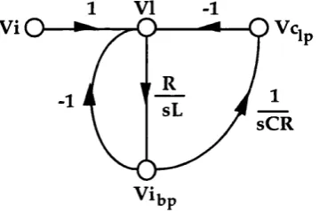
Vr VI
Vc
Fig 2.2-1 Simple RLC Filter
The voltage form ed across the capacitor 'C represents a 2nd order lowpass response, governed by the equation (2.2.1)
If the current 'i' flowing through the inductor L' is considered, this represents a 2nd order bandpass response, governed by the equation (2.2.2)
“ 2 R T~ (2.2.2)
In bo th equations the cut-off and centre frequencies, are determ ined by the reactive elements, L' and 'C w hile the Q of the filter is independently
determ ined by the resistive (loss) element, 'R'. If the filter became 'loss less', that is if R ^O , then Q-^o®.
To gain some insight into how a passive filter prototype m ay be designed and ultim ately fabricated into an integrated filter, the above circuit m ay be represented as a state-variable equivalent circuit using the Signal Flow G raph (SPG) m ethod [15,16]. By using the state equations as current flowing through the inductor and voltage developed across the capacitor, the
equation (2.2.3) describes the RLC filter of Fig 2.2-1.
^bp
V i-V r-V c,^ _ V i - y R - ^
sL sL
ibp = ---; ^ ^ --- 7 - ^ (2-2.3)
1 VI 1 VI
Vi Vci
Vr
sC
Vi Vc
-R
sC
(a) (b)
Fig 2.2-2 SFG of RLC Filter (a) N odal Representation of Equation (2.2.3) (b) Equivalent
In the active sim ulation of this circuit, the currents are represented as voltage signals by m ultiplying the current nodal variable i^^ by a resistive
scaling factor R, as show n by Fig 2.2-3.
VI -1
Vi Vg
sL
sCR
Fig 2.2-3 State-Variable voltage representation of an RLC Filter Prototype
By representing the RLC prototype using state-variables, a filter architecture w ith low pass and bandpass voltage outputs is achieved. The troublesom e inductor is replaced by a active integrator w ith a tim e constant t= L /R . The cutoff and centre frequencies of the filter are determ ined by the integrator
VI
Vi Vci
1+sL/R
sCR
Fig 2.2-4 State-Variable representation of an RLC Filter w ith Lossy Inductor
In the context of a continuous time (CT) integrated filter, the cutoff and bandpass centre frequency w ould be subject to foundry tolerances of fabricated com ponents and operating conditions. Thus, the design of the active integrator building blocks has an additional requirem ent of tunable tim e constants.
2.3 Active Tunable Integrators
2.3.1 Voltage Amplifier (Op Amp) Method
The sim plest im plem entation of an active integrator is the use of an operational amplifier (op-amp) as show n by Fig 2.3.1-1, w hich has the classical integrating response given by equation (2.3.1.1) and its Laplace Transform by equation (2.3.1.2).
Vout = — — f V in.dt
CRJ (2.3.1.1)
Vout =
OVout
(a)
Vin
O
-1
sCR
Ô
Vout
(b)
Fig 2.3.1-1 (a) Classical Active RC Integrator (b) SFG R epresentation
Since the fabricated com ponent is the integrating capacitor 'C w hich is subjected to foundry tolerances, the resistor is required to vary in ord er to m aintain a constant This w as first im plem ented by Banu & Tsividis [17] as a MOSFET device operating in its triode region, as show n by Fig 2.3.1-2a and 2.3.1-2b.
Vc
V i n Q
Vc
Fig 2.3.1-2 (a) Small-signal active RC integrator w ith variable time constant (b) Equivalent circuit element replacement
Vc2
R2
V c i
V i n Q
R1 ■QVout
Vin
O
- A o
1+sC / R2
V out (b)
Fig 2.3.1-3 (a) Lossy Tunable Integrator (b) SFG R epresentation
w here the voltage gain Ao= R2/R1 and the tim e constant x=CR2.
The active realisation of the passive RLC filter pro to ty p e of Fig 2.2-1 using the MOSFET-C m ethod is show n by Fig 2.3.1-4.
Vc2
R2
J-L
V ci
R1
V in Q
R1
C Rl
« 4 Î
V ci
R1
Fig 2.3.1-4 Active 2nd O rder Filter using the MOSFET-C approach
of the triode region MOSFET as a linear resistor directly in the signal path introduces considerable distortion [18].
2.3.2 Transconductance Am plifier Method
An alternative approach from the voltage am plifier m ethod w as the
introduction of the transconductance am plifier as the active building block for integrators is show n by Fig 2.3.2-1.
o-Vin
O
Fig 2.3.2-1 Symbol for a Transconductance Amplifier
The transconductance am plifier is in essence a voltage to current converter w ith a first order transfer characteristic given by equation (2.3.2.1).
iout = Gm(Vin) (2.3.2.1)
w here the forw ard transconductance gain 'Cm ' is in A /V .
An ideal transconductance am plifier has infinite in p u t and o u tp u t im pedances, and as a consequence if the o u tp u t is unloaded the effective voltage gain becomes infinite. If the o u tp u t of a transconductance amplifier is loaded by a capacitor, as show n by Fig. 2.S.2-2, a Transconductance-C integrator is formed.
Y in
O
O V o u t
V in G m C m
sC
(a)
Ô
V o u t
(b)
The corresponding transfer characteristic is given by equation (2.3.2.2).
Vout = — Yin
sC (23.2.2)
w here the tim e constant T=C/G m .
If the load capacitor is subject to a foundry tolerances, the tim e constant m ay be m aintained at its appropriate value by the adjustm ent of the forw ard transconductance 'Gm', thus a fundam ental requirem ent of the
Transconductance-C m ethod is tunable Gm.
In addition, the use of a transconductance amplifier w ith the o u tp u t connected to the in p u t realises a linear grounded resistance of value R = l/G m as show n by Fig 2.3.2-3.
Gm
Vc
R = l/ Gm
Fig 2.3.2-3 Simulating a grounded variable resistor w ith a Tunable Transconductor
VinO Vout
Vin
0
Ao
1+sC / C m 2
(a)
Ô
Vout
(b)
Fig 2.S.2-4 (a) Lossy Tunable Transconductance-C Integrator (b) SFG Representation
w here the voltage gain A o = G m l/G m 2 and the time constant T=C /G m 2
The active realisation of the passive RLC filter prototype of Fig 2.2-1 using the Transconductance-C m ethod is show n by Fig 2.3.2-5.
V cl Vc2
V in Q
G m l
^V o
Gm2
G m l 'o
-G m l
V cl
Fig 2.3.2-5 Active 2nd O rder Filter using the Transconductance-C approach.
2.4 Higher Order Filters: Design Topologies
2.4.1 Cascade Approach
The realisation of active filters w ith an order greater than 2 m ay be achieved by connecting a num ber of 2nd order filter sections in cascade to provide an n th order filter response. This technique is called the cascade approach.
The general transfer function for any type of filter response m ay be
expressed as the p ro d u ct of 2nd order functions (sometimes referred to as biquads), as illustrated by Fig 2.4.1-1 and equation (2.4.1.1):
H(s) = H T .(s) = r iK ,
w s"+S '-- + col
Q i
(2.4.1.1)
V oi V out
V in V o l V o2
o
-Fig 2.4.1-1 Cascade Realisation of an nth O rder Transfer Function
The transfer function of the individual 2nd order sections is given by Tj(s). The gain of each section is defined by a constant k[ w here the coefficients «ij and «oi determ ine the type of 2nd order function Ti(s) needed to realise
an overall filter transfer function H(s), such as a low pass or bandpass response.
If the design of the 2nd order sections provide a low o u tp u t im pedance, or alternatively provide a high in p u t im pedance, then each section m ay be connected in cascade w ithout causing m utual interaction due to loading and the product of each 2nd order section Tj(s) w ould reliably realise the n^h order transfer function H(s).
understood, very easy im plem entation and efficient use of active elem ents, typically one active gain block p er pole pair. It uses a m odular approach and results in filters that show satisfactory perform ance in practice. This in the m ain m ay be due the fact th at the cascade approach is very easy w hen considering on chip tuning, since each 2nd order section is responsible for the realisation of only one pole pair (or zero pair), the realisation of the individual critical frequencies of the filter are de-coupled from each other. To illustrate this point, equation (2.4.1.1) m ay be restricted to describe a single 2nd order bandpass filter section as equation (2.4.1.2):
T.(s) = --- --- (2.4.1.2) s ' + s - ^ + tOoi
At the centre frequency of the bandpass filters, equation (2.4.1.2) reduces to equation (2.4.1.3):
% {coJ = K,Q, (2.4.1.3)
Thus, the m axim um gain of the 2nd order bandpass filter occurs at the centre frequency and for a given section gain, the Q for any given subsection of an n th ord er cascaded filter m ay be readily determ ined.
The m ajor disadvantage w ith this m ethod how ever, is an increased param eter passband sensitivity [27,28] of each 2nd order section, w hich becomes m ore severe as the order increases.
The cascade design, how ever is very flexible and this approach is general, in that an arbitrary transfer function can be realised w ith no restriction placed on the perm itted location of the poles and zeros.
2.4.2 LC Ladder Prototype A pproach
A m ethod which m ay be em ployed is the operational sim ulation of the LC ladder, w here the active circuit is configured to realise the internal
operation. Fundam entally, this m ethod is based on sim ulating the Signal Flow G raph (SFG) of the ladder w here all the voltages and currents are considered as signals w hich propagate through the circuit, as illustrated in section 2.2. By w ay of an example, the realisation of a general 4th order bandpass filter is considered.
Firstly, the 2nd order lowpass LC prototype is found from appropriate filter tables [29,30] or software [31] and transform ed using the standard m ethod to a 4th order bandpass as show n by Fig 2.4.2-1.
Vi
Rs LI
C l R1
0 - 1 l - c
Cl
(a)
1-0 C
2=-cü„Ll
LI C2
L2
= C entre Frequency
(b)
Vo. bp
(c)
Fig 2.4.2-1 (a) Passive 2nd order Lowpass LC Prototype (b) Lowpass to Bandpass Transformation (c) Passive 4th order Bandpass LC Prototype
VI Vc
Vo bp
Vo
Vi VI
-R
sL2 sCl]
-R
Fig 2A.2-2 (a) N odal Signals of 4th order Bandpass Filter (b) SFG R epresentation
1+sLl/R 1+sC lR
R=Rs=Rl
Vo
J + s L l/R
sL2
sC2R 1+sClR
(b)
Fig 2.4.2-S (a) Minimised SFG of 4th order LC bandpass Filter (b) Active Realisation using Integrators
Active filters sim ulating the behaviour of LC ladders have been found to have the low est sensitivities to com ponent tolerances and consequently are regarded as the m ost appropriate for filters w ith stringent requirem ents [32]. They have the additional advantage that they can draw on the w ealth of know ledge gained in the area of analysis and synthesis of lossless filters from the m any passive filters tables [29]. The disadvantage of this approach is that a passive LC prototype m ust, of course exist before an active sim ulation can be attem pted.
Flowever, despite the superior low passband sensitivity properties th at the ladder synthesis poses, the m ain difficulty is the lack of a well understood, reliable tu n in g m ethod. In contrast to the cascade approach, the problem arises in identifying w hich tunable com ponent is to be varied in order to correct an observed error in the transm ission characteristic. A lthough
2.4.3 Inductor Replacement Approach
An alternative m ethod to realise an active doubly term inated LC lad d er filter is by elem ent substitution, w here the inductors are replaced w ith an active sim ulation and inserted into the LC filter topology. The best know n m ethod for inductor sim ulation is th at using a gyrator [19,35].
A gyrator is a tw o port netw ork w hose in p u t im pedance is represented by equation (2.4.3.1):
Z l o a d ( s )
(2.4.3.1)
w here r is the gyrator resistance.
The custom ary circuit symbol for a gyrator is show n by Fig 2.4.3-1
VI V2
o—'
(a)
i2
O
I ^ ^ V2 VI j yl2V2 0 | ^ ^ 0 y 2 1 V l | V2
o—^ I—o
o
J
L
O
(b)
Fig 2.4.3-1 (a) Gyrator Symbol (b) Small Signal Equivalent Circuit
As show n by Fig 2.4.3-1 (b), the small signal equivalent circuit of a gyrator m ay be described by an adm ittance (y - param eter) transm ission m atrix given by equation (2.4.3.2):
iL ( y l l yl2 Y V l
,-y2i y z z J l v z , (2.4.3.2)
z . = ^ = -1 i2 -Y.load
il yl2y21V V 2; yl2y21
w here r ^ = l/ (yl2y21), if y l2 = y21 = Gm then r^ = l/G m ^
(2 .4 3 .3 )
Thus if Yjq3^(s)=sC then Zj^(s) w ould appear to be inductive as show n b y Fig
2.4.S-2.
V I
(a)
1
Fig 2.4.S-2 (a) Gyrator Simulation of a (b) grounded Inductor
Since m ost active gyrators have a comm on ground connection as show n by Fig 2.4.3-2, the sim ulated inductor w ould also be grounded. If a floating inductor is required in a filter prototype as show n by Fig 2.4.2-l(c) this w ould require the cascading of tw o grounded gyrators and a common capacitor as show n by Fig 2.4.3-3.
"1 )C 4 X t
c-0-4-0-V2 VI V2
(a) (b)
Fig 2.4.3-3 (a) Gyrator Simulation of a (b) floating Inductor
i l 12
VI V2
Fig 2.43-4 Gyrator Realisation using Transconductance Amplifiers
U sing the transconductance amplifier based gyrator of Fig 2.4.S-4 both g rounded and floating inductances can readly be realised as show n by Fig 2.43-5.
G m
G m V I
sC
Gm
G m G m
G m l
V2 V I
sC G m lG m
L = L =
Gm^
(a)
G m lG m
(b)
Fig 2.4.3-5 Transconductance-C Simulation of (a) grounded inductor and (b) floating inductor
By using the transconductor based active inductors show n by Fig 2.4.3-S (a) & (b), the doubly term inated passive LC bandpass filter of Fig 2.4.2-1 (c) m ay be realised by the substitution of the floating inductor LI and grounded
inductor L2. All the properties of ladder filters, such as of low passband sensitivity are preserved by using this approach, b u t all the draw backs including complex tuning are not' alleviated.
active elem ents w ith a corresponding increase of power.
2.5 Integrators : Characteristics and Lim itations 2.5.1 Ideal Integrator
Integrators form the basic building block to realise an active filter as
illustrated in the previous sections. A n ideal integrator transfer function is given by equation (2.5.1.1):
w here r is a time constant
As illustrated in section 2.3, the tim e constant t, of an integrator is form ed by an RC time constant w hen an operational amplifier based integrator is used, or the time constant may be form ed by C /G m w hen an operational transconductance amplifier (OTA) based integrator is used. In both cases a fabricated capacitor is needed.
Gain
OdB
Freq.(Log)
A
Phase
Freq.(Log) -90°
(b)
Fig 2.5.1-1 (a) Integrator A m plitude (b) Phase Response
The unity gain (OdB) frequency of the integrator corresponds to the cutoff frequency of a lowpass filter or the centre frequency of a bandpass filter.
2.5.2 Non Ideal (Practical) Integrator
In practice however, real integrators are form ed using transistors w hich exhibit finite f t and finite o utput conductance. This has the effect of
low ering the DC gain of the integrator from infinity and introducing high frequency poles. The non-ideal integrator transfer function m ay be described by equation (2.5.2.1):
H(s) =
(1 + ST, )(1 + ST2 )(1 + ST3 )....(1 + ST^ )
(2.5.2.1)
As a result of a finite DC gain, Aq the first pole resulting in the 1 /s term in
equation (2.5.1.1) has m oved from the origin of the real axis in the s-plane. The first pole now results in the term 1/(1+ST,). The other poles result from the tim e constants associated w ith parasitics form ed by internal nodes
From equation (2.5.2.1), the integrating action w ould be form ed at
frequencies above the first pole location, r, producing a -90° phase shift. The second pole, w ould add an additional -90° phase shift and likewise for the other high frequency poles. The region of effective integrator operation (ie
-90° phase shift) w ould lie betw een the first two pole locations. If the other poles are considered to be well outside this region (ie » T j then equation (2.5.2.1) m ay be sim plified to equation (2.5.2.2):
H(s) =
(1 + s t,)(1 + s t2) (2.5.2.2)
Here the first pole r, is referred to as the dom inant pole and the no n dom inant pole is form ed by T^. The practical OTA-C integrator w ith non ideal com ponents is show n by Fig 2.5.2-1 and its corresponding frequency response is illustrated by Fig 2.5.2-2.
V i n O Vout
Gm
Go
Ao = Gm/Go
Fpl = Go/ 27c(C+Cp) Fo = Gm/ 27c(C+Cp) Fp2 = Gm/ 27tCp
Gain
Fp2 Fpl
OdB
Freq.(Log) Fo
Phase
Freq.(Log)
-90
-180
Fig 1.5.2-2 (a) Practical Integrator A m plitude (b) Phase Response
Effect Phase Response Pole Closest to
Fo
Phase
Phase Shift less than -90°
"Phase Lead"
-90 PI
Fo Frequency
Phase
Phase Shift greater than -90°
"Excess Phase"
-90 P2
Fo Frequency
Phase
Phase Shift "90 at Fo, but with gradient
-90 Equi-distant
Frequency
Table 2.5.2-1 Effect of pole spacing on phase shift of Integrator
Gm
Go
VI V2
Gm
Go
Fig 2.5.2-S 2nd order Resonator realisation using practical Transconductance Amplifiers
The ideal adm ittance matrix for the gyrator is derived by equation (2.4.3.2) and re-arranged to give equation (2.5.2.3):
Y
-^ ideal ~
" 0 Gm^
^-Gm 0 J (2.5.23)
H ow ever, considering that the resonator is constructed from non-ideal (practical) transconductance amplifiers, show n by Fig 2.5.2-3 w hich exhibit finite DC gain resulting in finite o u tp u t conductance. Go and the presence of excess phase shirts, 0 in the forw ard transconductance gain, Gm, the
adm ittance m atrix for a non-ideal gyrator is described by equation (2.5.2.4):
r
Ypractical Go
-Gme Go
(2.S.2.4)
This has two effects, firstly the unity gain frequency Fo of the gyrator is no longer dependent upon the G m /C as illustrated by equation (2.5.2.5):
Gm G m / C
(2.5.2.5) C + Cp 1 + C p / C
capacitance, C which for high frequency designs should be as small as possible, this effect can be corrected by some form of tuning.
In addition, the state variable filters show n by Fig. 2.3.1-4 and Fig 2.3.2-S indicate th at the Q of the respective filters should be determ ined purely by a ratio of fabricated com ponent param eters, such as resistance or
transconductance. However, as a result of the parasitic capacitance, Cp each transconductance am plifier exhibits excess phase %, resulting in Q
enhancem ent, creating Q errors [19,37,38] an d the first order relationship determ ining Q is no longer valid. To determ ine the real Q of the resonator circuit of Fig 2.5.2-3, the adm ittance m atrix of equation (2.5.2.4) is evaluated. By m aking the following assum ptions th at 0 « 1 and G m » G o for
yload=jcüC, then the in p u t adm ittance w ould approxim ate to equation (2.5.2.6):
yin = 2Go - 4-ja)C-j (2.5.2.6)
coC coC
w hich contains a negative real term proportional to excess phase, 0 .
If a further assum ption is m ade, that for a first order co = G m /C , then
equation (2.S.2.6) can be re-arranged to give an expression for Q, by equation
(2.5.2.T):
= {2.52.7)
Q Gm
Furtherm ore, the sensitivity of Q to excess phase, 0 can be obtained by differentiating equation (2.5.2.7) to give equation (2.5.2.S):
S g = ^ = 0 Q (2.52.8)
/0
Theoretically this parasitic capacitance could be absorbed into the total integrating capacitance value, this how ever presents several problem s.
The parasitics are not accurately known. In aggressive high frequency designs [13] in which the parasitics form a large part of the integrating capacitor, this problem m eans an increased uncertainty in the integrating capacitance value. A lthough autom atic frequency and Q tuning w ould be used, this is complicated if integrators do not exhibit a low phase error. Phase correcting netw orks m ay be em ployed to cancel the phase error of the non dom inant pole b u t these usually w ork "exactly" at a given frequency (ie centre frequency) and the rem aining error increases as one m oves aw ay from this given frequency, this can lead to significant Q error in the filter response.
The presence of parasitics can w orsen capacitance m atching accuracy and in turn leads to increased integrator m ismatch. For the best m atching, the proportion of parasitic capacitance to the total integrating capacitance, C p /C should be kept the same for each integrator [39], this requires very detailed foundry m odelling.
Parasitics do not track the m ain integrating capacitor well [40] in the presence of fabrication process variations. This once m ore increases integrator
m ismatch, unless the proportion of parasitic capacitance is kept to a m inim um . In addition, the parasitics are in general non-linear. This can cause distortion as well as dependence of the frequency response on the signal am plitude and pow er supply voltage.
2.5.3 Transconductance - O p A m p Integrator
The troublesom e parasitic capacitance, Cp at the o u tp u t of a
transconductance amplifier can be forced to a near ground potential by using a scheme called the Transconductance-C Op Am p integrator as illustrated by Fig 2.5.3-1
V i n O
O V o u t
virtual earth
Fig 2.5.3-1 Transconductance-C Op Amp Integrator
This schem e is in essence a com bination of both the Voltage A m plifier and Transconductance Amplifier integrator. By connecting a tunable
transconductor at the in p u t of the high gain voltage amplifier (Op Am p) the integrating action is still determ ined by G m /C . This scheme has been
successfully em ployed in the designs of a num ber of high frequency (up to 20MHz) CT filters [41].
The m ain advantage of em ploying the transconductance-C op am p integrator is that the parasitic capacitance connected at the o u tp u t of the transconductance am plifier is now at a near ground potential (ie virtual earth). Since there w ould be very little voltage change across the parasitics their effects w ould be greatly reduced. In addition, since the o u tp u t of the transconductor is connected to a virtual earth, its o u tp u t does not require to provide large voltage swings. The dem anding requirem ent of a low o u tp u t conductance of the transconductance w ould also be relaxed since the o u tp u t is now connected to a virtual earth.
am p integrator w ould inevitably lead to a greater pow er dissipation, despite the fact th at the pow er dissipation of the individual elem ents w ould be reduced due to relaxed perform ance requirem ents. M oreover the b an d w id th of the Op-amp w ould be required to be m uch greater than that of the the integrating action form ed by G m /C w hile at the sam e tim e providing a high voltage gain, A to m aintain the virtual earth, w ithout w hich the benefits of such a scheme are questionable. Thus, for very aggressive high frequency designs, the m inim isation of the num ber of internal nodes using the transconductance approach is favoured.
2.6 A utom atic T u n in g
To m anufacture a practical integrated filter w ith its com ponent tolerances, some form of fine tuning is unavoidable. As dem onstrated by sections 2.2 and 2.3, the filter frequency param eters are determ ined by RC products or C /G m ratios, which implies that to achieve accurate filter perform ance
absolute values of resistors, transconductors and capacitors m ust be realised.
Since the fabricated tolerances of com ponents are not sufficiently sm all to realise accurate filter perform ance, or as a result of varying operating
conditions, the generally adopted solution to this dilem m a is an autom atic electronic tuning scheme as p art of the total continuous tim e filter circuitry. This im plies that, in tuning, a m easurem ent of the filter perform ance is m ade, com pared w ith a standard, determ ining an error (if one exists) and finally applying a correcting signal, if required, to the filter, thus reducing the error, resulting in the desired filter perform ance.
A review of the literature [33-35,37,38,42-44] revels that the m ost reliable form of filter tuning firstly requires some form of reference signal or clock. From the filter response to this external reference signal at a given