www.ijaera.org 2017, IJA-ERA - All Rights Reserved 1
Determination of optical properties of the
GaAs thin layer by Photothermal Deflection
Technique
S. Ismail* & N. Yacoubi
Phothermal laboratory IPEIN, BP 62, Mrezka 8000, Nabeul, Tunisia Corresponding Author E-mail: [email protected]
Abstract: The paper deal with optical properties of multilayer structure using the Photothermal Deflection Technique. This structure is composed of four layers respectively GaAs, GaAlAs, GaAs and GaAlAs deposed on a substrate of GaAs. The third layer of GaAs (active layer) is doped with different concentrations of Zn, so we study the effect of Zn doped samples on the optical properties of the multilayer. Effect of Zn doped samples on the optical properties are undertaken. The optical absorption spectra for the different samples are obtained by comparing point to point the experimental curves of amplitude and phase of the Photothermal signal to the corresponding theoretical ones. A short shift in the energy gap of GaAs substrate is clearly detected.
Keywords: GaAs thin layer, PDS technique, Optical Properties, Optical Absorption Spectra
I. INTRODUCTION
The design of increasingly efficient electronic devices necessitated the use of semiconductors other than the silicon such as the GaAlAs/GaAs heterojunction [1]. The Gallium Arsenide (GaAs) is a chemical compound belongs to the III-V semiconductor family and has a direct band gap. Its symmetries have a zinc-blende form, while AlxGa1-xAs is obtained by substituting aluminium with
gallium. The crystal lattice parameter remains virtually the same [2]. The gap will be direct or indirect as a function of the introduced Al proportion x. This heterojunction has many advantages as firstly the relatively large band gap which allows operation at high temperature [3], then its high level of electronic mobility makes it possible to achieve good performances, moreover, the crystalline meshes are fairly close thus minimize the parasite recombination. The samples used in this study were prepared by the MOCVD technique [4 & 5], and have been doped with different concentrations of zinc in the active layer of GaAs. The paper aims to study the impact of doped Zn on optical properties of the GaAlAs/GaAs hetero structure using Photothermal Deflection Spectroscopy.
II. EXPERIMENTAL SET-UP
www.ijaera.org 2017, IJA-ERA - All Rights Reserved 2 Figure 1. Experimental device of Photothermal Deflection Spectroscopy technique
This deflection [7] is expressed by and can be written as:
) (
)
(
)
,
(
j te
z
t
z
III. THEORETICAL MODEL
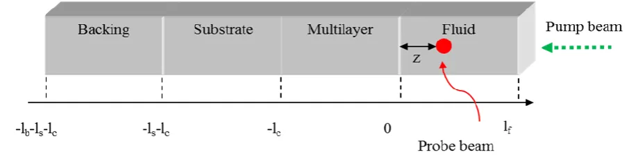
Figure 2 shows the arrangement of the sample in the experimental device above. A sample (multilayer + substrate) which thickness is (ls+lc) is fixed on a plexiglas backing which thickness is lb and both are
immersed in a quartz cell filled with Paraffin oil which thickness is lf.
Figure 2. Structure of the sample in the cell
As the incident light intensity is assumed to be uniform on the sample surface, the optical absorption of the sample will generate a one-dimensional heat flow.
www.ijaera.org 2017, IJA-ERA - All Rights Reserved 3
In the fluid
In the layer
In the substrate
In the backing
Where Ti and Di are respectively the periodic temperature and the diffusivity of the i media (i = f, c, s and b)
represents the heat source term
After solving the different heat equations, one can obtain the expression T0 of the periodic temperature
at the sample surface as found by other authors as Yacoubi et al [8], they demonstrated that the obtained T0 expression is function of optical properties of the sample.
IV. RESULTS AND DISCUSSION
The experimental variation of the normalized amplitude of the photothermal signal versus wavelength for different GaAlAs/GaAs samples for different Zn concentrations in the active layer are plotted on Fig. 3. We note that the amplitude decreases strongly in the middle region (858-938 nm) and saturates at high and low absorption regions. Moreover, these curves show also that the amplitude is sensitive to Zn concentration.
Figure 3. Plot of normalized experimental amplitude versus
Wavelength for Different Zn Doping
t
T
D
z
T
t
T
D
z
T
e
e
A
t
T
D
z
T
t
T
D
z
T
b b b s s s t j z c c c f f f
1
1
)
1
(
1
1
2 2 2 2 2 2 2 2 ) 1( ej t
z e
www.ijaera.org 2017, IJA-ERA - All Rights Reserved 4
On figure 4 are plotted the experimental phase variation with wavelength for the different samples. We notice as was obtained for the normalized amplitude a sensitivity of the phase to the Zn concentration. Table.1. summarizes the different phase shift obtained by figure 4.
Table.1. Phase shift for different Zn doping of the multilayer
Sample A B C D E
Zn doping ND 1.1018 5.1018 8.1018 10.1019
Phase shift i (°) 26 25.5 22.3 22 20
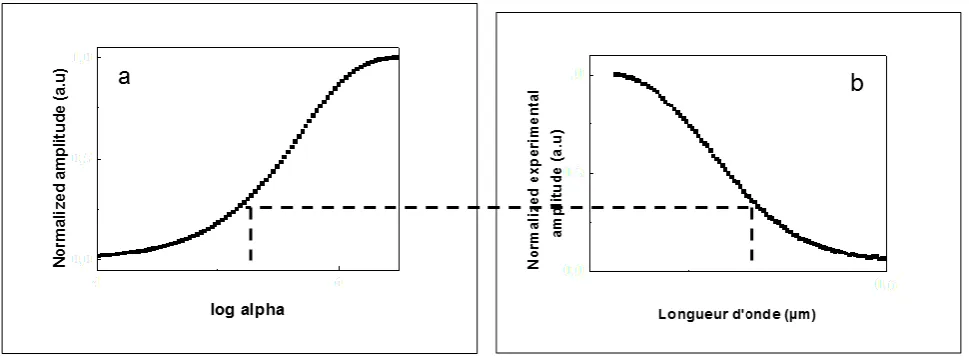
In order to determine the optical absorption spectrum of each sample, we have to compare the experimental normalized amplitude curve versus wavelength to the corresponding theoretical one versus optical absorption coefficient.
Figure 4. Phase difference (i)variation for the different samples
As indicated on the figure 5, for known value of the normalized amplitude, one can affect to each wavelength the corresponding optical absorption coefficient.
Figure 5. Normalized experimental amplitude versus absorption coefficient (a), normalized experimental amplitude versus wavelength (b).
www.ijaera.org 2017, IJA-ERA - All Rights Reserved 5
On figure 6 are plotted the curves representing the optical absorption coefficient versus energy for the different samples. These results can be used to extract the energy band gap of our different samples using the Tauc's law [9,10]:
( E)n = (E-Eg)
Where is a constant, Eg is the gap energy, n is equal to 2 for direct energy gap and equal to 1/2 for
indirect energy gap. In our case n = 2.
Figure 6. Optical absorption spectra for multilayer of GaAs/GaAlAs
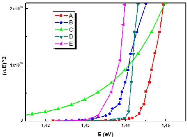
The exploitation of the curves given by Fig.6 using Tauc's method alloyed to plot (E)2 as a function of photon energy E for different samples as illustrated on Fig.7.
www.ijaera.org 2017, IJA-ERA - All Rights Reserved 6
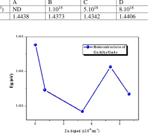
One can deduce the gap energy value by the intersection point obtained between the tangent of (E)² and the energy axis. The different values of energy gap obtained are reported on table.2. and plotted on Fig.8. to show the evolution of Energy gap versus Zn doped in the multilayer.
Table.2. Energy gap values for different Zn doping of the multilayer
Sample A B C D E
Zn doped (/cm-3) ND 1.1018 5.1018 8.1018 10.1018 Eg(eV) 1.4438 1.4373 1.4342 1.4406 1.4367
Figure 8. Variation of Eg as a function of different doping Zn
One can remark that the energy gap decreases with increasing Zn doping until a value of 5.1018cm-3 in Zn and then increase.
IV. CONCLUSION
In this paper, we studied a multilayer structure (GaAlAs/GaAs/GaAlAs/GaAs) on GaAs substrate doped with different concentrations of Zn from 0 to 1019cm-3on the active layer using for the first time
Photothermal Deflection Technique. The exploitation of normalized amplitude curves and phase shift curves versus wavelength by comparing with theoretical ones leads to obtain the optical absorption spectra and the mean value of the gap energy for each sample. The optical absorption spectra reaches a maximum value about 104cm-1. In addition, the gap energy decreases with increasing concentration of Zn doping until 5.1018 cm-3,then increases.
Conflict of Interest: The authors declare that they have no conflict of interest.
Ethical Statement: The authors declare that they have followed ethical responsibilities.
REFERENCES
[1] S. Moon, K. Kim,Y. Kim, J.Heo and J.Lee (2016), “Highly efficient single-junction GaAs thin-film solar cell on flexible substrate” .DOI:10.1038/srep30107
[2] K.K. Bajaj, D.C. Reynolds, C.W. Litton, Jasprit Singh, P.W. Yu, W.T. Masselink, R. Fischer, H. Morkoç (1986). Solid-State Electronics, vol. 29(2), pp. 215-227
www.ijaera.org 2017, IJA-ERA - All Rights Reserved 7 [4] Y.J. Jin, C.K. Chia, H.F. Liu, L.M. Wong, J.W. Chai, D.Z. Chi, S.J. Wang (2016). Applied Surface
Science, vol. 376, pp 236-240
[5] Youngjo Kim, Kangho Kim, Chang Zoo Kim, Sang Hyun Jung, Ho Kwan Kang, Won-Kyu Park, Jaejin Lee (2017) Solar Energy Materials and Solar Cells, vol. 166, pp 127-131
[6] A R.Warrier, K G.Deepa, T.Sebastian, C S.Kartha and K P Vijayakumar (2010). Thin Slid Films, vol.518(7), pp1767–1773.
[7] D. Ben Hlel, I. Gaied, N. Sghaier, A. Gharbi, H. Fitouri, N. Yacoubi, Analysis of optical and thermal properties of thermally oxidized mesoporous silicon layers, Microporous andMesoporous Materials (2014), doi: ttp://dx.doi.org/10.1016/j.micromeso.2014.11.016
[8] N.Yacoubi, A.Hafaiedh, A.Joullié (1994). “Determination of the optical and thermal properties of semiconductors with the photothermal method” Appl.Opt. vol. 33, pp 7171-7174.
[9] Nader Ghobadi (2013) Band gap determination using absorption spectrum fitting procedure. DOI : International Nano Letters December 2013, 3:210.1186/2228-5326-3-2