A High Linearity VHF Programmable Gain LNA
Xu ChengIMECAS/ESIC, Beijing, P.R.China Email: [email protected]
Guiliang Guo and Yuepeng Yan IMECAS/ESIC, Beijing, P.R.China Email: {guoguiliang, yanyuepeng}@ime.ac.cn
Abstract—A VHF (30MHz-300MHz) band digitally
programmable low noise amplifier (LNA) has been implemented with a 0.25um standard CMOS process for VHF CMMB mobile TV tuners. Utilizing a T-match input network, input matching of more than a decade bandwidth is achieved across all gain settings. Adopting the multiple gated technique, gain flatness enhancement and capacitor reuse etc., the proposed LNA demonstrates 3 gain settings of 20dB, 6dB, -9dB with S11 below -12dB at every gain setting. At a power supply voltage of 2.5V, the LNA consumes less than 10mA current, -6dBm IIP3 and a Noise Figure (NF) of less than 2.9dB at 20dB gain setting over the VHF band.
Index Terms—LNA (Low Noise Amplifier), broadband, VHF (Very High Frequency) band, CMMB(China Mobile Multimedia Broadcasting), MTV (Mobile TV), multiple gated technique, gain flatness enhancement
I. INTRODUCTION
As the level of integration and the requirement of low power consumption increases, multi-mode multi-standard wireless chip sets are continuously developing to incorporate as much functions as possible to cover more consumer needs. In correspondence with the trend, the rocketing market of portable DTV applications, such as DVB-H, CMMB [12], has attracted more and more scientists and engineers to search for more efficient architectures to meet the booming needs. For search of a perfect solution to all DTV applications, a multi-standard compatible receiver is a must to cover different areas with diverse DTV standards. Mobile TV standards such as VHF-III (174 to 248MHz), CMMB VHF (30 to 300MHz), T-DMB and so forth are research target of this paper [11].
In the general architecture of DTV receivers, one of the most important tasks is to design a LNA(low noise amplifier) which fundamentally determines the sensitivity and dynamic range of the receivers as a whole. On one side of sensitivity , the LNA should possess a NF (Noise Figure) as low as possible; on the other side of dynamic range, a LNA with multiple gain settings is preferred over several individual LNAs with separate one gain settings on account of the area, power and cost etc. For the reasons above, a programmable gain LNA is proposed to cover VHF band DTV standards.
Since the VHF band (30MHz-300MHz) by itself is a decade bandwidth, a tons of other radio applications
which may interfere with DTV signals and DTV signals themselves must be handled with as little distortion as possible. However, recent products, papers and patents offers solutions which only cover only part of VHF band or cannot be tunable or programmable to meet the dynamic range needs. Therefore, high performance broadband LNAs are required to possess sufficiently high and programmable gain, low NF, high linearity and an excellent input matching at all gain settings. In this paper, we propose a novel noise cancelling LNA architecture which incorporates T-matching network, multi-gated technique, gain flatness technique and programmable gain designs.
II.BRIEF RESEARCH COMPARISON
The key design challenge for the LNA is to provide high and reasonably flat gain within the required bandwidth with acceptable input and output matching requirement. Since the conventional inductive source degeneration LNA is only a candidate for narrow band applications and thus, our research focus is on wideband LNA structures.
by the main transistor can be cancelled out by placing an auxiliary input voltage sensing amplifier in a feed-forward configuration to the main transistor. This leads to a theoretically excellent noise performance for the LNA. However, a relatively poor linearity is inevitable due to the cascading of the amplification stages including the source follower, which is used as a crucial part of the combining network at the output node, and the nonlinearity of the auxiliary voltage-sensing amplifier. In conclusion, the main issue to be solved for noise cancelling LNAs is the relatively poor linearity. Taking the exemplifications above into account, we propose a programmable linearity enhanced noise cancelling LNA with gain flatness enhancement.
III.CIRCUIT DESIGN
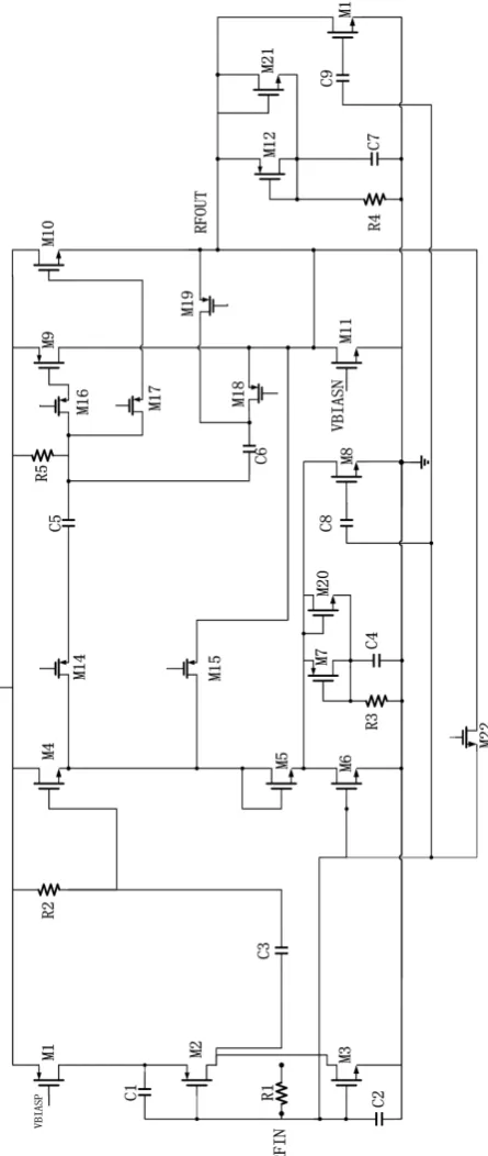
The novel LNA was designed and fabricated in TSMC 1P5M 0.25um CMOS process. It is a single sided LNA with digital gain control switches. Fig.1 shows the general schematic diagram of the LNA (biasing not shown). This circuit contains a first noise cancelling stage and a second source follower or a common source stage (it is changed via switching schemes). For the sake of clear illustration of its operating mechanism, we redraw the first noise cancellation stage in Fig.2.
A. Noise Cancellation Mechanism
Noise cancellation scheme was first proposed by F.Bruccoleri[1] and researched over the past ten years. Since this structure is in itself wideband and low in noise and distortion, papers and patents frequently cite it and offer a tons of modifications or highlights to it. In the broad view of LNAs, in the sub-1GHz frequency range, noise cancelling LNA is especially popular in almost every wireless application. Therefore, a general overview of the noise cancellation mechanism is given below.
In the noise cancelling stage as depicted in Fig.2, thermal noise with flicker noise generated by M2 and M3 (M2 and M3 are current reused structure for the goal of higher transconductance.) are eliminated at the source node of M4 through two signal paths of M2/M3/R1/C3/R2/M4 and M6. In detail, the first path comprised of (M2/M3/R1/C3/R2/M4) generates a noise voltage source that is opposite in phase with respect to the one generated by the second path (M6) while the signals generated by the two path are in phase. Therefore, we may obtain an ideal noise cancellation scheme without any deterioration of signals by properly scaling the aspect ratios of the devices on the two paths. Since the VHF (Very High Frequency) band covers frequency low to 30MHz, flicker noise should be taken into consideration for better theoretical guidelines to lower noise figure in the low frequency band.
In Fig.2, The input impedance can be calculated as follows,
(
1) (
2)
2 3
1
/ / 1/
/ / 1/
(
)
in
m m
Z
sC
sC
g
g
⎛
⎞
≈
⎜
+
⎟
⎝
⎠
(1)Where
Z
in is the input impedance of the noise cancellingstage.
g
m2 andg
m3 are respectively thetransconductance of M2 and M3.
C
1 andC
2 are new capacitors introduced to help in input matching, which are not shown in any papers or patents for the special case of VHF band applications. (On the issue of input matching, we first extract all parasitic capacitors/resistors/inductors of the input pad with ESD protection and model the bond-wire with the help of electromagnetic software HFSS. Then we put all models above into the Cadence Spectre in search of an excellent input matching. Post-simulation results reveal thatC
1and
C
2 are pivotal to input matching in VHF band.) The noise current of M2 and M3 is given by2
, 2
4
, 2n M d M
K
i
kT g
f
f
f
γ
=
Δ + Δ
(2)2
, 3
4
, 3n M d M
K
i
kT g
f
f
f
γ
=
Δ + Δ
(3) Where the first parts are channel thermal noise of M2/M3 and the second parts are flicker noise of M2/M3.k
is the Boltzmann constant andg
d M, 2/g
d M, 3 are respectivelydrain conductance of M2/M3.
γ
is the process noise parameter andK
is an experiential parameter. Withinput impedance matching and noise cancelling requirement, we can easily obtain
2 3
1
(
)
s m mR
g
g
=
+
(4)1 2
2
m1 (
)
s
R
g
R
= +
(5)Where
R
s is the source impedance.g
m2 andg
m3 arerepectively the transconductance of M2/M3. As seen in equations above, channel thermal noise and flicker noise of first input matching stage can be easily cancelled by properly choosing the
g
m2 of the second stage of theamplifier. Upon noise cancellation and input matching conditions, the noise figure of the LNA in Fig.2 can be written as
2 3
2 1 1 1 1 1
2
1
1
4
8
s s s s s
R
R
R
R
KR
NF
R
R
R
R
kTR
f
γ
⎛ ⎞
⎛
⎞
= + +
⎜ ⎟
+ ⋅
⎜
+ +
⎟
⋅
⎝ ⎠
⎝
⎠
(6)Where
R
s is the source impedance.k
is the Boltzmannconstant.
γ
is the process noise parameter. K is an experiential parameter. Therefore, the noise figure can be lower than 3dB by increasingR
1 and the noise issue islower the output resistance and weaken the shielding effect of cascading transistors. However, M5 provides a relatively low resistance node which is in correspondence to the linearity enhancement technique such as multiple gated technique executed by M8 and the gain flatness enhancement technique done by R3/C4/M17/M20. More detailed explanations will be given in following exemplifications of techniques adopted.
B. Linearity Analysis
On the aspect of distortion issue, an LNA with a single gain setting is of no practical use taking into account the unconditionally high peak to average ratio of OFDM signals. Thus a programmable gain LNA with three gain settings of 20dB/6dB/-9dB is proposed and its programmability is explained as below. We introduce a bypass path constituted by M22 and a second stage switched by M14/M15/M16/M17/M18/M19 between two work modes of common source stage (M9/M11) and source follower stage (M10/M11). What is more, we introduce a reusable capacitor C6 which is connected between the gate and drain terminals of M9 in common source mode while in source follower mode, C6 is connected between the gate and source terminal of M10 via switching switches M16/M17/M18/M19. In a more specific manner, the common source stage indicates that M14/M16/M18/M19 are on, M15/M17 are off while the source follower stage hints that M14/M17/M19 are on and M15/M16/M18 are off. In these two cases, M15 is off in order to isolate the first noise cancellation stage from the output node and, thus, the whole LNA works as a two stage amplifier. In the case of common source stage, the M9/M11 help introduce a gain peak which is higher than the one generated by the first noise cancelling stage and therefore, two gain peaks combine to generate a more flat gain over the VHF band. Besides, C6 forms a miller capacitor which brings in a feed-forward path and a zero around M9. Thus, high frequency linearity is enhanced. In the other case of source follower stage, C6 is extremely important as it increases the gate-source capacitor of M10 and a feed-forward path is also generated. A distinctive point here is that drain resistance is generally much higher than source resistance for transistors and consequently, the same feed-forward capacitor generates totally different poles and zeros! In conclusion, C6 is reused in common source and source follower modes in search of higher linearity and gain flatness.
As to the issue of linearity enhancement, we adopt subthreshold region transistors M8/M13 as a multiple gated technique proposed by Tae Wook Kim[6] et al. As depicted in Fig.3, we simulate two transistors which are respectively biased at saturation region and subthreshold region. It is easy to find that the third order derivatives of the two transistors are opposite in phase. Therefore, we can combine the outputs of saturation transistors and subthreshold transistors in order to cancel out their third order nonlinearity terms as depicted in Fig.4. Gm1 and Gm2 are used to represent the saturation transistor and subthreshold one since transistors are generally referred to as basic transconductor cells. The outputs are
combined in Fig.4, in which their high order nonlinear terms are cancelled by proper dimensioning the ratio of Gm1/Gm2. As in Fig.1, we only need to adjust the biasing points and width/length ratios of M8/M13 in order to enhance the whole linearity performance. Simulated IIP3 is offered in Fig.6 and it is clear that around 9dB increase in IIP3 is obtained through the use of multiple gated transistors (MGTR stands for multiple gated transistors).
For the consideration of clear mathematical derivations, we replace M7/M20/R3/C4 with a current source
i
2b and M6 with a current sourcei
2a as depicted in Fig.5. The nonlinearity current of M2a and M2b can be expressed asi
2a=
g
2a,1V
gs,2a+
g
2a,2V
gs2,2a+
g
2a,3V
gs3,2a (5)i
2b=
g
2b,1V
gs,2b+
g
2b,2V
gs2,2b+
g
2b,3V
gs3,2b (6) And the relation ofV
gs,2aandV
gs,2b can be modeled asV
gs,2b= −
c
1V
gs,2a+
c
2V
gs2,2a+
c
3V
gs3,2a (7) As a result, the current flows through M3 is
2 2
3 2 2 2 ,1 1 2 ,1 ,2 2 ,2 1 2 ,2 2 2 ,1 ,2
3 3
2 ,3 1 2 ,3 3 2 ,1 2 2 2 ,2 ,2
(
)
(
)
(
2
)
M a b a b gs a a b b gs a
a b b b gs a
i
i
i
g
cg
V
g
c g
c g
V
g
c g
c g
c c g
V
= + =
−
+
−
−
+
−
−
−
(8) M2b replicates the drain current of M2a and partially compensates the nonlinearity of M2a. R and C forms a filter structure to provide more design freedom.
In addition, the low resistance output node generated by diode-connected M5 is of significance in the multiple gated technique on account of the possible current sink generated by M8. If the node is a high resistance one, the current sink by M8 may vary the voltage level of the output node and even change the working region of output transistors. In this design, the voltage level of output node keeps relatively stable across all process corners and temperature variations. Therefore, a stable yield is guaranteed in this design.
C. Gain Flatnes
As to the final technique of gain flatness enhancement, we propose a novel CMOS-R-C structure constructed by M7/M20/R3/C4 or M12/M21/R4/C7. This structure seems as a gyrator and in fact, it is a gyrator in some frequency band. Fig.7 shows the general schematic of CMOS-R-C structure and we can calculate the general input impedance as follows,
Fig. 1 General schematic of LNA core without biasing
Fig. 2 General schematic of the noise cancellation stage
2 3 4 ,1 1,1 2,1 3,1 4,1
outp m inp m inp m inp m inp
I
= +
g V g V g V g V
+
+
+
…
2 3 4
,1 1,1 2,1 3,1 4,1
outn m inn m inn m inn m inn
I
= +
g V g V g V g V
+
+
+
…
2 3 4
,2 1,2 2,2
-
3,2 4,2outn m inn m inn m inn m inn
I
=
g V g V g V g V
+
+
+
…
2 3 4
,2 1,2 2,2 3,2 4,2
outp m inp m inp m inp m inp
I
=
g V g V g V g V
+
+
+
+
…
1,1 1,2
( + )(
)
out m m inp inn
I g g V V
=
−
Fig. 4 The nonlinearity cancellation scheme
,2 gs a
V
i
2ai
2b,2 gs b
V
Fig.5 Concept of post distortion cancellation
Fig. 6 IIP3 comparison of traditional noise cancelling LNA and MGTR LNA
a
in
V
C
gs1 m1 1g V
1 o
r
C
gs2 2 2 mg V
2 o
r
R
C
1
V
1
V
V
2b
Therefore, we can have a negative impedance (an active inductor-like structure!) at some frequency band simply by setting the first part of equation (9) to a negative impedance value. This idea follows the gain flatness technique offered by Yueh-Hua-Yu et al[5]. In reference [5], an inductor is introduced to split the output dominant pole and push the resulting complementary poles out to higher frequency. In this design, the active inductor not only split the output dominant pole but also is in parallel with output resistance and capacitance. Thus, an LC tank composed of inductors and capacitors appears at the output node and a gain peak is generated at some high frequency band. Hence, the gain flatness can be enhanced at the expense of quicker gain roll-off at higher frequency due to the complementary poles. What is more, the active inductor is connected to ground in one side while it still owns voltage headroom. Therefore, the working status of main noise cancellation stage amplifier is not affected while a small portion of output current is reused to help in linearity and gain flatness enhancement. Measurement results prove the explanations above. In one word, taking area consumption into considerations, an active inductor is proposed and applied in the gain flatness technique. Measurement results show very flat gain curves in three operating modes and validate the design. What is more, the CMOS-R-C structure provides some filtering which enhances linearity over the VHF band, which is also shown in simulations. In conclusion,
the CMOS-R-C structure is valuable in both the gain flatness and linearity issues.
IV.CHIP FABRICATION AND MEASUREMENT RESULTS
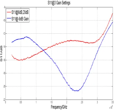
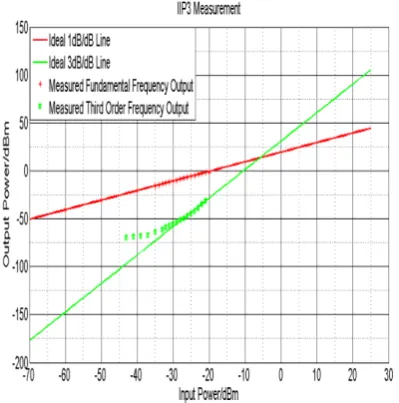
The VHF programmable LNA was implemented in TSMC 0.25um CMOS process and was taped out in June 2012. The chip photograph is shown in Fig.8 and its size is 0.76*0.53mm2 since no inductors are on chip. The signal is input from the left side and output from the lower right side. Measurement results demonstrate three S11 lower than -12dB as is depicted in Fig. 9. Since 20dB/6dB power gain settings share almost the same input stage, we thus only plot one S11 for both of them for clearness and two S11 curves remain. The S21 is shown in Fig. 10 and three gain settings of 20dB/6dB/-9dB are perceptible. The S21 curves fall down a little above 290MHz. The NF (noise figure) is less than 2.9dB @S21=20dB as in Fig. 11 while the IIP3 is -5.76dBm @S21=20dB as shown in Fig. 12. IIP3 is measured with two input signals located at 165MHz and 167MHz. Under the supply voltage of 2.5V, The LNA consumes less than 10mA current. In the layout design, considering the possibly large area occupied by MIMCAPs Insulated-Metal Capacitors), we use MOSCAPs (Metal-Oxide-Semiconductor Capacitors) as much as possible without degrading the LNA performance.
Fig. 8 The chip photograph of the VHF programmable LNA
V.CONCLUSIONS
This programmable gain LNA is the first ever LNA designed specifically for VHF CMMB applications and own a relatively large dynamic range with high linearity. What is more, this LNA exhibits a good gain flatness over the decade bandwidth with relative low noise figure under the current consumption of less than 10mA. Capacitor reuse and CMOS-R-C structure is proposed in this design. Although the frequency band covered by the LNA is relatively not wide enough compared to recent research achievements, the LNA is still an engineering oriented design and will be fully used in future VHF CMMB products. As to products recently offered such as AD803 and AD102 etc., this LNA is capable of meeting the needs of CMMB VHF apparatus. According to linearity figures-of-merits (FOMs) defined as
10*log(OPI3(mW)/Pdc(mW))
, we make a general comparison in Table I.Fig. 10 Three power gain settings of S21=20dB, 6dB, -9dB.
Fig. 11 Noise Figure of Pre-simulation and Post-simulation @maximum power gain S21=21dB.
Fig. 12 IIP3 @maximum power gain S21=20dB with two input signals located at 165MHz and 167MHz.
TABLE I.
PERFORMANCE COMPARISON TABLE OF WIDEBAND LNA
Refere
nce [1] [2] [3] [4] [7] This work Frequ
ency/ MHz
2~160
0 54~880 40~900 100~930 174~240 30~300
Gain/
dB 13.7 22 20.3 13 15/-10 20/6/-9 NF/d
B 2.5 2.8 4 4 2.2 2.9
IIP3/d
Bm 0 -21 -10.8 -10.2 -15 -5.76 OIP3/
dBm 13.7 1 9.5 2.8 0 15.24
Power
/mA 14 23 23.9 0.6 N/A 10
Techn ology/ um
0.25 0.18 0.18 0.13 0.18 0.25
FOM 0.67 0.03 0.207 2.646 N/A 1.33
ACKNOWLEDGMENT
This work was supported by state key 863 project “Wireless Measurement and Control Technique, Equipment and System Research and Development Based on Wireless Industrial Access”. Great thanks to all staff to members of ESIC in IMECAS.
REFERENCES
[1] F.Bruccoleri et al., “Wide-band CMOS low noise amplifier exploiting thermal noise cancelling”. JSSC. pp.275-282,Vol.39, Feb. 2004
[2] S. Lou et al., “A wideband CMOS variable-gain low-noise amplifier for cable TV tuners,” Proc. IEEE ASSC. Nov. 2005.
[3] D.R Huang et al., “A 40-900MHz broadband CMOS differential LNA with gain-control for DTV RF tuners,” Proc. IEEE ASSC., Nov. 2005.
[4] S.B.T.Wang et al., “ Design of a sub-mW 960MHz UWB CMOS LNA,” JSSC., vol. 41, no. 11, Nov. 2006.
[5] Yueh-Hua Yu et al., “A Compact Wideband CMOS Low Noise Amplifier With Gain Flatness Enhancement”, JSSC.,vol.45, March 2010.
[6] T.W.Kim et al., “Highly linear receiver front-end adopting MOSFET transconductance linearization by multiple gated transistors”, IEEE J. Solid-State Circuits, vol.39, no.1, pp.223-229. Jan. 2004.
[7] Seong-do Kim et al., “A Fully Integrated CMOS Low-IF Mobile-TV Tuner for Band-III T-DMB/DAB Applications”, IEEE ICACT, pp2199~2202, Feb. 2009. [8] Donggu Im, IIku Nam, Kwyro Lee, “A Low Power
Broadband Differential Low Noise Amplifier Employing Noise and IM3 Distortion Cancellation for Mobile Broadcast Receivers”, IEEE Microwave And Wireless Components Letters, Vol.20, No.10, pp566~568, Oct. 2010. [9] Song-Ski Song, Dong-Gu Im, Hong-Teuk Kim and Kwyro
Tuner Applications”, IEEE Microwave And Wireless Components Letters, Vol.18, No.2, pp118~120, Feb. 2008. [10]Yuna Shim, Chang-Wan Kim, Jeongseon Lee and Sang-Gug Lee, “Design of Full Band UWB Common-Gate LNA”, IEEE Microwave And Wireless Components Letters, Vol.17 No.10, pp721~723S, Oct. 2007.
[11]I.Vassilios et al., “A 65-nm CMOS multistandard, multiband TV tuner for mobile and multi-media applications,” IEEE J.Solid-State Circuits, vol.43, no.7, pp/1522-1533, Jul. 2008.
[12]M. Jeong et al., “A 65-nm CMOS low-power small-size multistandard, multiband mobile broadcasting receiver SoC,” in IEEE ISSCC Dig. Tech. Papers, Feb. 2010, pp.460-461.
Xu Cheng received B.S in University of Electronic Science and
Technology of China. He is now pursuing his doctoral degree in Institute of Microelectronics, Chinese Academy of Sciences. His major research interest is radio frequency modules such as LNA, Mixer etc. and analog signal designs. Nowadays he is researching on low power RF transceivers for wireless sensor networks, wireless industrial access and so forth.
Gui-Liang Guo received B.S in Beijing Institute of Technology
and Ph.D degree in Institute of Microelectronics, Chinese Academy of Sciences. His major research interest is radio frequency transceivers and SOC designs. He is now industrializing commercial mixed signal chips for home apparatus and so forth.
Yue-Peng Yan received the M.S. degree in electrical and