RESIDENTIAL STATIC VAR COMPENSATORS
by
Muhammad Kamran Latif
A dissertation
submittedinpartialfulfillment oftherequirementsforthedegreeof
DoctorofPhilosophyinElectricalandComputerEngineering BoiseStateUniversity
DEFENSE COMMITTEE AND FINAL READING APPROVALS
of the Dissertation submitted by
Muhammad Kamran Latif
Dissertation Title: Demand-Side Load Management Using Single-Phase Residential Static VAR Compensators
Date of Oral Examination: 6th December 2019
The following individuals read and discussed the dissertation submitted by student Muham-mad Kamran Latif, and they evaluated the presentation and response to questions during the final oral examination. They found that the student passed the final oral examination.
Said Ahmed-Zaid, Ph.D. Chair, Supervisory Committee
Nader Rafla, Ph.D. Co-Chair, Supervisory Committee
Thad Welch, Ph.D. Member, Supervisory Committee
John Stubban, Ph.D. Member, Supervisory Committee
Milorad Papic, Ph.D. External Examiner
I sincerely thank my advisor, Dr. Said Ahmed-Zaid, for his supervision, guidance, and advice during the entire course of this research work. Dr. Ahmed-Zaid’s unflinching encouragement and endless support inspired me during my stay at Boise State University (BSU). I would also like to thank my committee members Drs. Nader Rafla, Thad Welch and John Stubban for their guidance, constructive critique and advice during the project work.
Furthermore, I would like to acknowledge the Department of Electrical and Computer Engineering (ECE) at BSU for allowing me to use various departmental facilities that helped in carrying out the research efficiently as well as for giving me the opportunity to teach and instruct the Microprocessor class and lab during various semesters.
Additionally, I would also like to thank Avista Utilities for their support during this research. Especially, I would like to acknowledge Randy Gnaedinger and Reuben Arts at Avista Utilities for their support of this research project.
I am grateful to all the members of the research lab, especially, Danyal Mohammadi and Andr´es Valdepe˜na for their continuous support and fruitful discussions. Moreover, I would like to extend my gratitude to Luka Daoud and Ziyang Liang with whom I have collaborated in several research projects.
Finally, I am extremely thankful to my family for their boundless love and unwavering support during my the Ph.D. journey. This work is dedicated to all of you.
Distribution systems are going through a structural transformation from being radially-operated simple systems to becoming more complex networks to operate in the presence of distributed energy resources (DERs) with significant levels of penetration. It is predicted that the share of electricity generation from DERs will keep increasing as the world is mov-ing away from power generation involvmov-ing carbon-emission and towards cleaner energy sources such as solar, wind, and biofuels. However, the variable behavior of renewable re-sources presents challenges to the already existing distribution systems. One such problem is when the distribution feeder experiences variable power supply due to the unpredictable behavior of renewable resources. Therefore, it becomes difficult to maintain end-of-line (EOL) voltages within an acceptable range of the ANSI C84.1 Standard.
Moreover, electric utility companies consider Conservation by Voltage Reduction (CVR) as a potential solution for managing peak power demand in distribution feeders. Con-servation by Voltage Reduction is the implementation of a distribution voltage strategy whereby all distribution voltages are lowered to the minimum allowed by the equipment manufacturer. This strategy is rooted in the fact that many loads consume less power when they are fed with a voltage lower than nominal. Therefore, by implementing CVR, utility companies can potentially reduce the peak power demand and can delay the up-gradation of the distribution feeder assets. To maximize the benefits from CVR, the whole distribution feeder must participate in regulating power to lower the demand during hours of demand. Hence, there is a need for a local solution that can regulate residential voltage levels from
Such a solution will not only provide flexibility to electric utilities for better control over residential voltages but it can also maximize the benefits from CVR.
This dissertation presents the concept of a closed-loop Residential Static VAR Compen-sator (RSVC) that will allow electric utility companies to locally regulate the voltage across the distribution feeder. The proposed RSVC is a novel smart-grid device that can regulate a residential load voltage with a fixed capacitor in shunt with a reactor controlled by two bi-directional switches. The two switches are turned on and off in a complementary manner using a pulse-width modulation (PWM) technique that allows the reactor to function as a continuously-variable inductor. The proposed RSVC has several advantages compared to a conventional thyristor-based Static VAR Compensator (SVC), such as a quasi-sinusoidal inductor current, sub-cycle reactive power controllability, lower footprint for reactive com-ponents, and its realization as a single-phase device. The closed-loop RSVC contains two regulation control loops: the primary control loop regulates the customer load voltage to any desired reference voltage within ANSI C84.1 (120 V nominal±5%) and a secondary loop adjusting the reference voltage to track the point of minimum power consumption by the loads. This approach to CVR has the merit of adapting to the nature of the customer load, which may or may not decrease its energy consumption under a reduced voltage. This local approach to voltage regulation and CVR is a radical departure from current CVR strategies that have been in existence for over 30 years but have not been widely adopted by electric utilities due to high costs and technical challenges.
ABSTRACT . . . v
LIST OF TABLES . . . xiii
LIST OF FIGURES . . . xiv
LIST OF ABBREVIATIONS . . . xxii
1 Introduction . . . 1
1.1 Overview . . . 1
1.2 Research Motivation . . . 8
1.2.1 Conservation by Voltage Reduction (CVR) . . . 9
1.2.2 Traditional Methods for CVR Implementation . . . 12
1.2.3 Minimum Power Point Tracker (MinPPT) / Optimal Operational Power Tracker . . . 13
1.3 Proposed Solution – Residential Static VAR Compensator (RSVC) . . . 15
1.4 Organization of the Dissertation . . . 17
2 Operating Principles of Residential Static VAR Compensators . . . 19
2.1 Fundamental Principles of AC Power Flow . . . 19
2.2 Effect of Shunt Reactive Power Compensation . . . 21
2.3 Reactive Power Compensation Techniques . . . 25
2.4 Static VAR Compensators (SVCs) . . . 28
2.5 SVC Characteristics . . . 29
2.5.1 SVC Characteristics in a Power System . . . 32
2.6 Thyristor-controlled reactor (TCR) . . . 33
2.6.1 Principle of operation . . . 34
2.6.2 Harmonic Analysis for TCR Current . . . 36
2.6.3 Three-Phase Thyristor-Controlled Reactor . . . 40
2.7 Thyristor-Switched Reactor (TSR) . . . 43
2.8 Thyristor-Switched Capacitor (TSC) . . . 44
2.8.1 Principle of Operation . . . 44
2.8.2 Dynamic Response with Multiple TSCs . . . 44
2.9 An Efficient Switched-Reactor-Based Static VAR Compensator . . . 47
2.9.1 PWM-Based Switched Reactor . . . 47
2.9.2 Switching the Current Harmonic Distortion for the PWM-Based Switched Reactor . . . 50
2.9.3 Input Current Harmonic Distortion for PWM-Based Switched Re-actor . . . 52
2.9.4 The Reactive Power Capability of a PWM-Based Switched Reactor with a Fixed Capacitor . . . 53
2.9.5 Design Example . . . 54
3 Bi-Directional Solid State Switches in Residential Static Var Compensators (RSVCs) . . . 57
3.1 Bi-Directional Switches Topologies . . . 57
3.2 Current Commutation Problem Between Bi-directional Switches . . . 61
3.4 Current Commutation Based on the Voltage Across the Bi-directional Switches 66 3.5 Commutation of Current Between Bi-Directional Switches in the
Residen-tial Static VAR Compensator . . . 69
4 Performance Analysis and Simulation Results of the Residential Static Var Compensator . . . 70
4.1 RSVC Open-Loop Design Using Matlab/Simulink . . . 70
4.1.1 Design of the Four-Step Current Commutation State Machine Based on the Sign of Voltage Across the Bi-Directional Switches . . . 71
4.1.2 Design of the Residential Static VAR Compensator (RSVC) . . . 76
4.2 RSVC Open-Loop Simulation and Performance Analysis . . . 78
4.2.1 Voltage Waveforms . . . 78
4.2.2 Current Waveforms . . . 79
4.3 Performance Analysis of Open-Loop RSVC . . . 80
4.3.1 Output (load) Voltage Variation With Duty Cycle . . . 80
4.3.2 Reactive Power Variation With Duty Cycle . . . 80
4.3.3 Input and Output Power Variation With Duty Cycle . . . 82
4.4 RSVC Closed-Loop Design . . . 84
4.4.1 Design of Voltage Regulation Control Loop . . . 84
4.4.2 Integrator Windup in the PI controller . . . 86
4.5 Performance Analysis of Voltage Regulation Control Loop . . . 88
4.5.1 Tracking the Reference VoltageVre f . . . 88
4.5.2 Voltage Regulation Loop Performance With Variable Input Voltage 90 4.5.3 Load Power Demand Shaving in a Distribution Feeder . . . 93
4.7 Performance Analysis of Power Regulation Control Loop . . . 99
4.7.1 Tracking the Power for a 2 kW Resistive Load . . . 99
4.7.2 Tracking the Power for a Resistive Heater Load . . . 100
4.7.3 Tracking the Power for a Resistive Heater Load with Variable Input Voltage . . . 102
4.7.4 Tracking the Power for Loads with Negative CVR Factor . . . 103
4.7.5 Performance of Power Regulation for Combined (Spot) Loads . . . . 106
5 Design Implementation on SoC and Experimental Results . . . 111
5.1 Open-loop SoC Design for RSVC Gating Signals . . . 111
5.2 Open-loop Experimental Testing Results . . . 114
5.2.1 Input and Output Voltage . . . 114
5.2.2 Input (Source) Current . . . 115
5.2.3 Reactor Current . . . 117
5.2.4 Current through the bi-directional switch . . . 117
5.2.5 Output (Load) Voltage Variation with Duty Cycle . . . 119
5.2.6 Input and Output Power Variation with Duty Cycle . . . 119
5.3 Closed-loop Design for RSVC . . . 121
5.3.1 SoC Implementation . . . 122
5.4 Design of Voltage Regulation Control Loop . . . 123
5.4.1 Tracking the Reference VoltageVre f . . . 124
5.5 Design of Power Regulation Control Loop . . . 126
5.5.1 Tracking the Power for the Resistive Load . . . 126
VAR Compensators . . . 131
6.1 Peak Shaving on IEEE-13 Node Feeder using RSVCs . . . 134
6.2 Peak Shaving on an Actual Feeder using RSVCs . . . 137
6.2.1 Distribution Feeder Description . . . 137
6.2.2 Load Model . . . 138
6.3 Power and Voltage Profile for the Distribution Feeder . . . 139
6.4 A General Way of Approaching Peak Shaving Using CVR . . . 142
6.4.1 Changing the Substation LTC and Voltage Regulator Tap Settings . . 142
6.5 Peak Shaving Using Single-Phase RSVC . . . 145
6.5.1 Simulation Method . . . 145
6.5.2 Simulation Results . . . 147
6.6 Cost Analysis and Performance benefits for Peak Shaving between RSVC and BESS . . . 151
7 Conclusion And Future Work . . . 154
7.1 Applications for Deploying the RSVC . . . 155
7.1.1 Conservation of Power by Voltage Reduction (CVR) . . . 156
7.1.2 Mitigation of Voltage Violation . . . 156
7.1.3 Distribution Systems Assets Deferral . . . 157
7.1.4 Peak Shaving During Peak-Demand Hours . . . 157
7.1.5 Power Factor Correction . . . 157
7.1.6 Increasing the Hosting Capacity . . . 158
7.2 Suggested Future Work . . . 158
REFERENCES . . . 162
1.1 CVR factorCV Rf of different customer classes. . . 11 1.2 ZIP values for common household loads. . . 14
3.1 Comparison of different bi-directional switches topologies. . . 60 3.2 Non-hazardous combinations for current commutation based on the
direc-tion of load current. . . 65
4.1 PI controller and saturation block parameters for the voltage regulation loop. 86
5.1 RSVC components used in the laboratory prototype. . . 114
6.1 LTC and voltage regulator settings in the feeder without CVR. . . 138
7.1 RSVC Suggested Power Electronics Components For Future Designs (lab-prototype). . . 159
1.1 Average annual growth rates of the world renewables supply from 1990 to
2016. . . 2
1.2 One-day wind power profile plotted with 1-minute average. . . 3
1.3 Voltage variation due to change in solar irradiance for a solar plant in rural Idaho, USA from 6 AM till 1 PM plotted with 1-sec time interval. . . 4
1.4 ANSI C84.1 standard voltage levels. . . 5
1.5 Voltage profile for a typical distribution feeder. . . 6
1.6 Voltage profile for a distribution feeder with an LTC. . . 7
1.7 Voltage-dependent energy consumption of a Dell LCD. The plot shows the real and reactive power consumption, Pm and Qm respectively, while op-erated between 100V and 126V, whereas the red line indicates the voltage response curve using the least-square fitted ZIP values,PeandQe. . . 14
1.8 An overview for the proposed control system for the closed-loop RSVC containing two regulation loops, namely the “Voltage Regulation Control Loop” and the “Power Regulation Control Loop”. . . 16
2.1 Power transfer between two power sources. . . 20
2.2 Variable reactive power source connected in shunt with the load. . . 22
2.3 Phasor diagram of an electrical grid during nominal operation. . . 22
2.4 Phasor diagram of an electrical grid during under-voltage operation with reactive shunt compensation. . . 24
reactive shunt compensation. . . 25
2.6 Radial AC system without reactive power compensation. . . 27
2.7 Radial AC system with shunt reactive power compensation. . . 27
2.8 Radial AC system without reactive power compensation. . . 28
2.9 Radial AC system with series reactive power compensation. . . 28
2.10 Different Configurations of Static VAR Compensator. . . 30
2.11 An ideal Static VAR Compensator. . . 31
2.12 V/I characteristics of an SVC having a fixed capacitor and variable reactor. . 31
2.13 V/I characteristics of an SVC having a fixed capacitor and variable reactor with operating points for given power systems. . . 33
2.14 Thyristor-Controlled Reactor (TCR). . . 34
2.15 Voltage and current waveforms in a TCR for different thyristor gating angles. 35 2.16 Variation of the TCR susceptanceBTCRwith firing angleα. . . 38
2.17 Harmonics in the TCR current. . . 40
2.18 Total Harmonic Distortion (THD) for the TCR current. . . 41
2.19 A delta-connected three-phase TCR. . . 41
2.20 Switching operation of a TSC. . . 45
2.21 V/I characteristics of a multiple TSC with operating points for given power systems. . . 45
2.22 PWM-based switched reactor . . . 48
2.23 The circuit for calculating the input currentiin,nharmonics. . . 53
2.24 Single-phase PWM-based switched reactor with fixed capacitor. . . 54
2.25 The reactive power provided by the PWM-based switched reactor with a fixed capacitor compensator. . . 56
3.2 A simplified RSVC circuit to explain the problems with conventional switch-ing methods. . . 62 3.3 A circuit for understanding current commutation based on load current. . . . 63 3.4 Four-step switching state machine for two bi-directional switches based on
output load current. . . 65 3.5 Positive voltage-based current commutation from SW1 to SW2 when the
current direction is positive. . . 67 3.6 Positive voltage-based current commutation from SW1 to SW2 when the
current direction is negative. . . 67 3.7 Four-step switching state machine for two bi-directional switches based on
the voltage polarity across the bi-directional switches. . . 68
4.1 Circuit diagram of the Residential Static VAR Compensator. . . 71 4.2 Top-level block diagram for the state machine producing gating signals for
the bi-directional switches. . . 72 4.3 A complete state machine for producing gating signals SW 1A, SW 1B,
SW 2A and SW 2B based on the output load voltage. The states (blocks) in the state machine represents the output of the state machine for each state. . . 73 4.4 Output of the switch SW 1A from the state-machine for a complete cycle
of the output voltage. . . 74 4.5 The gating signals for current commutation from SW1 to SW2 based on
the amplitude of voltage when output voltageVout>0. . . 75
the amplitude of voltage when output voltageVout<0. . . 75
4.7 The RSVC Simulink model with a fixed capacitor and a switched inductor having bi-directional switches. . . 76
4.8 Bi-directional switches model in Simulink. . . 77
4.9 Input (source) and output (load) voltage waveforms at duty cycle D = 0.5. . 78
4.10 Input (source), output (load) and inductor current waveforms at duty cycle D = 0.5. . . 79
4.11 Output (Load) voltage variation with duty cycle (D). . . 81
4.12 Net reactive power (QSVC) variation with duty cycle (D). . . 82
4.13 Input and output power variation with duty cycle (D). . . 83
4.14 Block diagram of the feedback system for the voltage regulation loop of the Residential Static VAR Compensator. . . 85
4.15 Block diagram for clamping method to avoid integrator windup. . . 87
4.16 Block diagram for back-calculation method to avoid integrator windup. . . . 88
4.17 Voltages (input, output and reference) and reactive power change caused by the voltage regulation loop operation for an ideal input voltage. . . 89
4.18 Real powers (input and output) and duty cycle change caused by the voltage regulation loop operation for an ideal input voltage. . . 90
4.19 Voltages (input, output and reference) and reactive power change caused by the voltage regulation loop operation for a variable input voltage. . . 91
4.20 Real powers (input and output) and duty cycle change caused by the voltage regulation loop operation for a variable input voltage. . . 92
by voltage regulation loop operation for a variable input voltage to achieve
peak-demand shaving. . . 94
4.22 Real powers (input and output) and duty cycle change caused by voltage regulation loop operation for a variable input voltage to achieve peak-demand shaving. . . 94
4.23 Complete Simulink block diagram of power regulation loop. . . 96
4.24 Block diagram of Power Loop P/O Decision subsystem. . . 97
4.25 Block diagram of Accumulator subsystem. . . 99
4.26 Voltages (input, output and reference) and real power (input and output) change caused by power regulation loop operation for an ideal input voltage with a 2 kW purely resistive load. . . 101
4.27 Net reactive power and duty cycle change caused by power regulation loop operation for an ideal input voltage with a 2 kW purely resistive load. . . 101
4.28 Voltages (input, output and reference) and real power (output) change caused by power regulation loop operation for an ideal input voltage with a resis-tive heater load. . . 102
4.29 Net reactive power and duty cycle change caused by power regulation loop operation for an ideal input voltage with a resistive heater load. . . 103
4.30 Voltages (input, output and reference) and real power (output) change caused by power regulation loop operation for a variable input voltage with a resistive heater load. . . 104
4.31 Net reactive power and duty cycle change caused by power regulation loop operation for a variable input voltage with a resistive heater load. . . 104
4.32 An example of the load whose power increases as the voltage decreases. . . . 105
by power regulation loop operation for an ideal input voltage with a load
having negative CVR factor. . . 107
4.34 Net reactive power and duty cycle change caused by power regulation loop operation for an ideal input voltage with a load having negative CVR factor. 107 4.35 Voltages (input, output and reference) and real power (output) change caused by power regulation loop operation for an ideal input voltage with a spot load. . . 108
4.36 Net reactive power and duty cycle change caused by power regulation loop operation for an ideal input voltage with a spot load. . . 109
4.37 Change in power for individual loads as the voltage varies. . . 109
5.1 Complete block diagram for System-on-Chip implementations for generat-ing the gatgenerat-ing signals. . . 113
5.2 Laboratory prototype of Residential Static VAR Compensator (RSVC). . . . 114
5.3 Experimental result for input (source) and output (load) voltage waveforms at duty cycle D = 0.5. . . 115
5.4 Experimental result for input (source) current at duty cycle D = 0.5. . . 116
5.5 Harmonic analysis of the input (source) current. . . 117
5.6 Experimental result for inductor current at different duty cycles. . . 118
5.7 Experimental result for current through top switch at different duty cycles. . 118
5.8 Experimental results for output (load) voltage variation with duty cycle (D). 120 5.9 Experimental results for input and output power variation with duty cycle (D). . . 120
plemented in the Zedboard and dSPACE platform. . . 122
5.11 Zynq-7000 SoC implementation of the state machine on processing logic (PL) and the timer interrupt on processing system (PS) for the development of the closed-loop RSVC on Zedboard. . . 123
5.12 Voltage regulation loop implemented in Simulink/dSPACE. . . 123
5.13 Plots of RSVC laboratory prototype with voltage regulation loop test results. 124 5.14 Power regulation loop implemented in Simulink/dSPACE. . . 126
5.15 Complete control system for an RSVC laboratory prototype in Simulink/dSPACE.127 5.16 Plots of RSVC laboratory prototype with voltage regulation loop test results. 128 5.17 Plots of RSVC laboratory prototype with voltage regulation loop test results. 129 6.1 Single-line diagram for the IEEE-13 node test feeder. . . 134
6.2 Voltage profile for the IEEE-13 node feeder with and without RSVCs. . . 135
6.3 Peak power demand as function of the number of RSVCs. . . 136
6.4 Feeder lines and voltage (pu) for the distribution feeder. . . 138
6.5 Annual power demand profile for the distribution feeder. . . 140
6.6 Yearly voltage profile for the distribution feeder. . . 141
6.7 Winter power demand profile for the distribution feeder. . . 141
6.8 Maximum and minimum voltage across the distribution feeder at different tap settings for the substation LTC and in-line voltage regulator. . . 143
6.9 Winter power demand profile for the distribution feeder at different tap settings. . . 144
6.10 Flowchart for RSVC deployment strategy based onWorst-offender algorithm.146 6.11 RSVC placement in the distribution circuit. . . 147
settings for LTC and in-line voltage regulators is set to 116 V. . . 148 6.13 Long-term RSVC-enhanced CVR power profile for the distribution feeder. . 149 6.14 Short-term RSVC-enhanced CVR power profile for the distribution feeder. . 150 6.15 Net reactive power provided by the RSVC devices during their operation
for the entire year. . . 150 6.16 Transformer Deferral Calculation . . . 152
A.1 Periodic Pulse Function with an Amplitude of 1, time period of T and pulse width ofTp. . . 171
AMI – Advanced Metering Infrastructure
ANSI – American National Standards Institute
CVR – Conservation by Voltage Reduction
DERs – Distributed Energy Resources
EMF – Electromagnetic Force
EOL – End-of-Line
FACTS – Flexible AC Transmission Systems
FC-TCR – Fixed-Capacitor with Thyristor-Controlled Reactor
LTC – Load Tap Change
MinPPT – Minimum Power Point Tracker
MPPT – Maximum Power Point Tracker
P&O – Perturb and Observe
PLL – Phase-Locked Loop
PV – PhotoVoltaic
PWM – Pulse Width Modulation
RSVC – Residential Static VAR Compensator
STATCOM – STATic synchronous COMpensator
TCR – Thyristor-Controlled Reactor
THD – Total Harmonic Distortion
TSC – Thyristor-Switched Capacitor
TSR – Thyristor-Switched Reactor
VVO – Volt-VAR Optimization
CHAPTER 1
INTRODUCTION
1.1
Overview
of all existing coal generation plants more expensive than building new local renewable energy [2]. It is estimated that by 2040 the share of electricity generation from renewables will increase from 25% today to around 40% worldwide [3].
Figure 1.1: Average annual growth rates of the world renewables supply from 1990 to 2016 [1].
power increased again to about 3,300 MW at 5 pm. This graph points to the variability and unpredictability associated with power generation using wind as a renewable fuel. Similar behavior for variation in PV output power as a function of voltage can be observed in Figure 1.3. The voltage is measured at the point of common coupling of a solar plant connected with the electric grid in rural Idaho, USA. The voltage level fluctuates between 120 V to 124 V during the daytime due to the change in solar energy. Similar voltage variations due to fluctuations in solar irradiance can also be found in [5].
Figure 1.2: One-day wind power profile plotted with 1-minute average [4].
6:00 AM 7:00 AM 8:00 AM 9:00 AM 10:00 AM 11:00 AM 12:00 PM 1:00 PM
Time (hours)
118 119 120 121 122 123 124 125
Voltage (V)
Figure 1.3: Voltage variation due to change in solar irradiance for a solar plant in rural Idaho, USA from 6 AM till 1 PM plotted with 1-sec time interval.
becomes imperative to research devices which can keep a consistent balance between power generation and demand at the consumer side of the power system.
Figure 1.4: ANSI C84.1 standard voltage levels [7].
within a minimum voltage of 114 V at the secondary side of the distribution transformer to a maximum of 126 V. The end-user equipment should be designed to operate at full performance within the service voltages limits of Range A (generally, the tolerance for the end-user equipment is from 110V (120 V minus 10%) to 126 V (120 V plus 5.0%)). Therefore, electric utility companies plan their distribution systems based on the voltage limits within Range A of the standard. However, with the variability associated with renewables and due to the variations in the nature of the loads connected to the distribution feeder throughout the year, it becomes challenging to maintain a voltage profile within the ANSI standards.
Figure 1.5: Voltage profile for a typical distribution feeder.
However, due toI2Rpower losses, the poor power factor of loads, and variations of loads throughout a day (or a season), customers experience less voltage than the voltage at the source of the distribution feeder. Generally, customers at the end of the distribution feeder face a significantly lower voltage than the customers closer to the feeder. A typical voltage profile for a distribution feeder is shown in Figure 1.5. It can be seen that the end-of-line voltage is below 114 V, which is the minimum permissible voltage level according to the ANSI standard.
Figure 1.6: Voltage profile for a distribution feeder with an LTC.
of service voltage outside the ANSI standard include the use of capacitor banks, in-line voltage regulators, decreasing I2R power losses by increasing the conductor size, and transferring loads to another feeder.
1.2
Research Motivation
Modern reactive power compensation techniques use Flexible AC Transmission Systems (FACTS) devices that provide dynamic reactive power to the power system. FACTS de-vices are high-speed power electronics dede-vices that combine advanced control system techniques with the fast processing power of embedded microprocessors to respond to the reactive power needs of the power system [8, 9]. Commonly-used FACTS devices are Static VAR Compensators (SVCs) and inverter-based STATic synchronous COMpensators (STATCOMs). For utilities, FACTS technology has become an essential tool to alleviate certain problems associated with the scheduling of reactive power and to get the most service from their transmission and distribution networks by enhancing grid reliability [10]. This research focuses on developing a FACTS device for regulating residential volt-ages. The dissertation introduces a novel idea of the Residential Static VAR Compensator (RSVC), an improved FACTS device, based on the traditional Static VAR Compensators, with the following observations:
• With the advancement in high-power transistor devices such as MOSFETs and IG-BTs, the role of FACTS devices has become critical for an electric utility in dis-tribution systems. RSVC devices can provide a real-time (active) reactive power compensation, therefore, facilitating the integration of renewables in the distribution system and regulating the voltage levels at the customer location.
Residential Static VAR Compensator is to develop a device which helps to reduce power consumption during peak hours to save energy and costs by lowering customer voltage to a lower voltage level, commonly known as Conservation of power by Voltage Reduction (CVR), but still maintaining a relatively flat voltage profile across the distribution feeder.
• A localized approach to conservation of power by voltage regulation has the merit of adapting to the nature of the customer load, which may or may not decrease its energy consumption under a reduced voltage. This local approach is a radical departure from current CVR strategies, which have been in existence for over 30 years, but have not been widely adopted by electric utilities due to high costs and technical challenges.
Therefore, the development of RSVC will assist in the integration of DERs, provide a mechanism to effectively implement CVR across the distribution feeder and conform to the nature of individual load(s). The following sections will introduce CVR and its benefits from the studies published in the literature. A separate section will highlight the importance of understanding the nature of the loads and signify the importance of a localized CVR instead of conventional approach of implementing CVR.
1.2.1 Conservation by Voltage Reduction (CVR)
CVR effectiveness is measured by the CVR factor. The real power CVR factor is defined as the ratio of the percentage of the real power saved to the percentage of the voltage reduction used to achieve power saving. The CVR factor,CV RP, can be represented in mathematical form as given in Equation (1.1),
CV RP=
∆P% ∆V%
(1.1)
where ∆P% is the percentage of real power saved and ∆V% is the percentage of voltage
reduced. Electric utilities employ CVR for short-term demand response management as well as for long-term power reduction. For short-term CVR, the voltage is reduced for a short duration to reduce the peak-demand and for long-term, the voltage is reduced permanently to save power.
Electric utilities have long-known the advantages of distribution voltage reduction. In the 1970s, due to petroleum fuel shortages, electric utilities began investigating the effects of reducing the voltage at the customer level as a method for energy conservation. In 1973, American Electric Power (AEP) conducted a study to examine the impact of voltage reduction on the loads. Their test results showed significant savings by reducing the level of residential voltages. In the study conducted by AEP, the voltage levels were reduced by 5% for four hours. In one of the distribution feeders under consideration, a 5% voltage drop for 4 hours a day, from 9 AM to 1 PM, resulted in an immediate saving of 4% in the load power demand [13].
customer classes.
Table 1.1:CVR factorCV Rf of different customer class [14].
References Residential Commercial Industrial
California [15] 0.76 0.99 0.41
BPA [16] 0.77 0.99 0.41
AEP [12, 17] 0.61 0.89 0.35
CPUC [11] 1.14 0.26 N/A
SCE [18] 1.30 1.20 0.50
Snohomish [19] 0.33-0.68 0.89-1.10 N/A HQ [20] 0.06-0.67 0.80-0.97 0.10
NEEA [21] 0.63 0.37 N/A
Detroit [22] 0.96-1.11 0.75-0.80 0.50-0.83
A general conclusion can be drawn by looking at the CVR factors in Table 1.1, that reducing voltage results in energy savings. However, before lowering the voltage, electric utilities must understand the behavior of the loads under reduced voltages. Closed-loop loads (loads with control mechanisms to regulate their operational performance when the voltage is reduced) operate longer to give the same service when the voltage is reduced. Typical closed-loop loads consist of loads with thermostat/thermal cycles such as electric water heaters, and regulated constant power loads such as furnaces and ovens.
For electric utilities, CVR can become a tool for demand-side management. To sum-marize, the CVR benefits include a reduction in net power loss includingI2Rlosses in the transmission lines; reduction in eddy currents and hysteresis losses in the transformers; peak-load management without buying power from other utilities; delay in critical assets upgrade such as substation transformer and less fuel consumption thus helping the environ-ment.
1.2.2 Traditional Methods for CVR Implementation
Electric utilities often employ load tap change (LTC) transformers at the feeder source to implement CVR. As every distribution circuit has its load demand characteristics, it becomes difficult for electric utilities to impose a particular strategy for energy savings from one distribution feeder to another. When electric utilities apply CVR on a distribution feeder, the LTC transformer at the distribution substation decreases the feeder voltages. However, it becomes a challenge to keep the end-of-line voltage within an acceptable range. Due to voltage drops, utilities avoid reducing the voltage at the substation to the minimum permissible value and cannot get the maximum benefits from CVR at all points along the distribution network.
of capacitors for CVR purposes, however, one such reference [26] discusses the optimal capacitor placement for CVR purposes.
Closed-loop Volt-VAR Optimization (VVO) devices are more suitable for CVR appli-cation as they can determine the best voltage and VAR combination for a certain period and can adapt to dynamic changes in the loads. Specialized equipment and tools from Varentec [27], Gridco [28] and, Utilidata [29] are commercially available. Electric utilities have also employed Advanced Metering Infrastructure (AMI) meters-based VVO [30] and SCADA-based VVO [31] for CVR purposes.
1.2.3 Minimum Power Point Tracker (MinPPT) / Optimal Operational Power Tracker
CVR is an important tool for electric utilities to save energy, however the load composition has changed substantially by the turn of the 21st century. With the increase in the number of power electronics devices in households, such as phone and laptop chargers, flat-screen televisions, liquid crystal displays (LCD’s), plasma displays, etc., the behavior of the load has changed as the voltage varies [32]. A general perception is that the appliances consume less energy at reduced voltage. This might not be true given the complex nature of modern loads.
squared. In 2010, a study conducted by the Pacific Northwest National Laboratory (PNNL) reported the ratios for Z, I, and P for several household loads [33]. Table 1.2 summarizes the ZIP values for seven common household loads.
Table 1.2: ZIP values for common household loads [33].
Loads Z % I % P %
Incandescent Light Bulb (70W) 57.11 42.57 0.32 Magnavox Television (Cathode Ray Tube) 0.15 82.66 17.19
Oscillating Fan 73.32 25.34 1.35
Liquid Crystal Display (Dell) -40.70 46.29 94.41
Plasma TV (Sony) -32.07 48.36 83.71
Liquid Crystal Display (Clarity TV) 3.83 3.96 99.87 Compact Fluorescent Light (42W) 48.67 -37.52 88.84
Figure 1.7:Voltage-dependent energy consumption of a Dell LCD. The plot shows the real and reactive power consumption, Pm and Qm respectively, while operated between 100V
and 126V, whereas the red line indicates the voltage response curve using the least-square fitted ZIP values,PeandQe [33].
consumption increases by reducing the voltage. This can be seen in Figure 1.7, which shows the voltage profile for a Dell LCD. It can be seen that the power consumption increases as the voltage is reduced.
The reference [34] lists ZIP values for more residential loads, as well as for four different commercial customers that included a supermarket, a restaurant, a laundromat and an optical store. Among the commercial loads, the supermarket load had the one with the maximum P (constant power) element in the ZIP value because of the dominance of heating, ventilation and air conditioning (HVAC) systems. Therefore, for feeders and distribution circuits where CVR does not yield energy savings, an autonomous localized voltage tracking strategy should be adopted. Using such a strategy will ensure that the minimum power-point is tracked with modern loads that employ an abundance of switching power supplies and spot loads that contain a higher percentage of HVAC loads regardless of the voltage level.
1.3
Proposed Solution – Residential Static VAR Compensator (RSVC)
(CVR). As stated earlier, CVR relies on the idea that a percentage of the load on the distribution feeder will be of constant impedance. With a constant impedance load, if the voltage decreases, the power decreases. By decreasing the feeder power, the overall energy conservation will be improved. Therefore, the RSVC control system plays an essential role in controlling the reactive power provided by the device to the regulation bus.
To incorporate modern loads with switching power supplies and composite loads where a larger percentage is made of constant power loads, a minimum/optimal power point tracking is proposed in this dissertation. Hence, the overall control system for an RSVC will consist of two regulation loops. The objective of the first control loop will be to implement an inner voltage regulation loop for an RSVC and the goal of the second control loop will be to implement the outer power regulation loop for an RSVC. Figure 1.8 shows a simplified control systems design for an RSVC system. The voltage control loop acts as a faster control loop than the outer power minimization/optimization loop.
PI Controller RSVC Low Pass Filter Power Measurement Sensors Minimum Power Point Algorithm Reference Voltage (120V) Voltage Regulation Control Loop Power Regulation Control Loop Measured Voltage Voltage Reference Increment ( v)
RMS Voltage Measurment
Saturation Block (Limits Vrefto
114-126 )
The objectives intended to be achieved by the RSVC are given below:
• The device can regulate the customer load voltage at the desired reference level regardless of variable and fluctuating power injected by distributed energy resources.
• The device can minimize customer power consumption by tracking the optimal ref-erence voltage.
• The device does not generate substantial harmonics which might require filtering and incur more development cost.
• The device will have a relatively lower cost compared to existing competitive devices on the market, even though they operate using the same principles.
1.4
Organization of the Dissertation
This dissertation is organized into seven chapters. Chapter 2 provides an overview of the principles of reactive power compensation. Traditional VAR compensators are reviewed, with emphasis on a Thyristor-Controlled Reactor (TCR). A novel approach for reactor switching based on a PWM technique is described in this chapter. The drawbacks of TCR and advantages for a PWM-based reactor switching over a traditional thyristor angle firing switching are also discussed in the chapter.
of the current commutation through the bi-directional switches based on the voltage sign across the switches is explained.
Chapter 4 presents a detailed guide for simulating open-loop and closed-loop RSVC in Simulink. The chapter also shows the performance of the open-loop and closed-loop RSVC design. Simulation results showing the performance of the voltage regulation loop to track the reference voltage with normal and unstable input voltage are presented in this chapter. The chapter also shows the performance of the power regulation loop involving loads with positive and negative CVR factors and adjusting the reference voltage so that minimum power is utilized.
Chapter 5 presents the experimental setup for testing the laboratory prototype of the RSVC system. The performance of the open-loop RSVC laboratory prototype is analyzed and discussed on the basis of the experimental results. Moreover, the experimental results from the closed-loop RSVC testing and their performance with a resistive load are also presented.
Chapter 6 includes a case study for the deployment of RSVC in an actual distribution feeder to attain RSVC-enhanced CVR. It is shown that the peak shaving on the distribution feeder can be performed by deploying RSVC devices, which can provide an alternative to batteries commonly used for peak shaving and load demand management.
CHAPTER 2
OPERATING PRINCIPLES OF RESIDENTIAL STATIC VAR
COMPENSATORS
A Residential Static VAR Compensator (RSVC) is an improved smart-grid device which aims to solve power quality issues in distribution systems and residential feeders. This chapter focuses on the operating principles of the RSVC and its interaction with the dis-tribution and residential feeders based on understanding the power transfer between two single-phase sources in an AC power system. A brief review of the classical Static VAR Compensator (SVC) is also provided. The fundamental operating principle of the RSVC is to provide reactive power compensation with a superior performance than that of a classical SVC. The reactive power capabilities of the RSVC are also formulated and verified.
2.1
Fundamental Principles of AC Power Flow
In order to understand the operating principle of an RSVC, it is important to grasp the concept of AC power flow when there are two active energy sources in the system. Consider a power system as shown in Figure 2.1 with two energy sources labeled as EG and ER.
The energy source EG represents the power source (distribution/residential feeder) at the
P
s
Q
s
V
S∠
jX
V
R∠
0
Figure 2.1: Power transfer between two power sources.
The complex powers at the sending and receiving ends of the power system are,
SS=PS+jQS=VS
X(VRsinδ−jVRcosδ+jVS) (2.1)
SR=PR+jQR=VR
X (VSsinδ+jVScosδ−jVR) (2.2)
In the distribution system, the difference between the angle in the sending end voltage and receiving end voltage, power angleδ, is approximately equal to 0. It can be approximated that there there is no real power transfer between the two power sources since the δ =0. Equations (2.1) and (2.2) can be reduced to,
PS=PR=0 (2.3)
SS= jQS= jVS
X (VS−VR) (2.4)
SR= jQR= jVR
X (VS−VR) (2.5)
levels. From Equations (2.4) and (2.5), in the case where the sending end voltage is greater than the receiving end voltage, i.e.,VS>VR, then bothQSandQRare positive andQS>QR. This means that the reactive power flows from the sending end to the receiving end of the line. This case happens when a lagging or inductive current is flowing through the impedance X, therefore, resulting in a lower receiving end voltage. Similarly, when the sending end voltage is less than the receiving end voltage, i.e.,VS<VR, bothQSandQRare
negative andQS<QR. This implies that the reactive power flows from the receiving end to
sending end of the line. In this case, a leading or capacitive current is flowing through the impedance, which results in a higher receiving end voltage.
The change of the terminal voltages, ∆V =VS−VR, depends on the reactive power.
Equation (2.5) can be rewritten as,
∆V =VS−VR= X QR
VR (2.6)
where VS, VR and QR respectively show the sending end voltage, receiving end voltage
and the reactive power drawn at the receiving end of the power system. If∆V is positive,
then the difference in the terminal voltages can be minimized by decreasing QR, which increasesVR. This mode of operation is called a capacitive mode. If ∆V is negative, then QR is increased to minimize∆V, which decreasesVR. This mode of operation is called an
inductive mode.
2.2
Effect of Shunt Reactive Power Compensation
Consider a power system as shown in Figure 2.2. The power system is similar to the power system shown in Figure 2.1 except there is a switch connected in series with energy source
an energy source at the sending endEG with the voltage given byVS. This energy source is connected with a load,L, via a transmission line having line reactance given byX. The output voltage at the loadLis given byVR.
V
SjX
V
RE
GE
L O A D
L
SW
I
Figure 2.2:Variable reactive power source connected in shunt with the load.
For the reference case, consider that the variable reactive power source,E, is turned off, i.e., the switchSW is open. Therefore, the vector sum of the input voltage is given as,
#»
VS=V# »R+jX#»I (2.7)
V
REF
V
R
V
S
jXI
I
Figure 2.3: Phasor diagram of an electrical grid during nominal operation.
During this condition, the load voltage at the customer in the distribution feeder is at the required reference levelVREF.
To understand the effect of the shunt reactive power compensation using E, let’s con-sider the following two modes:
1. When the voltage at the receiving end is less than the reference voltage, i.e.,VR <
VREF. In this case, the variable reactive power source works in the capacitive mode to boost the load voltage. For example, this case is typical for customers at the end of the distribution feeder;
2. When the load voltage at the receiving end is greater than the required reference voltage, i.e.,VR>VREF. In this case, the variable reactive power source suppresses
the load voltage and works in the inductive mode. For example, this case arises when the electric utility implements CVR and the voltage at the feeder source needs to be dropped lower so that the entire feeder can participate in the CVR.
In the capacitive mode, the shunt energy source should inject reactive power to boost the load voltage. In other words, when switch SW is connected to the power system E
should behave as a capacitor. The reactive power injected will flow to the load, reducing the amount of reactive power supplied by the source, therefore decreasing the voltage drop across the transmission line and increasing the load voltage. In terms of the terminal voltages, without the reactive power source ∆V =VS−VR is positive. The ∆V can be
minimized by increasing theVR. This can be achieved by reducing the reactive power flow
in the transmission line by providing the reactive power the load consumes locally.
Figure 2.4 shows the phasor diagram of the system with the shunt reactive energy source. Without the reactive power source, the input current I lags the input voltageVS
the new reference voltageVREF,1. When the reactive energy source is added to the power system, it acts as the capacitor, thus making the input currentI1less inductive. As a result, the receiving end voltage is higher than the initial level.
V
REF,1
V
R
V
S
jXI
1
I
1
V
REF
I
I
c
Figure 2.4: Phasor diagram of an electrical grid during under-voltage operation with reactive shunt compensation.
In the inductive mode, the shunt energy source should absorb reactive power to decrease the load voltage. In other words,E should behave as an inductor so as to make the current flowing through the transmission line more inductive. The phasor diagrams of the power system with the shunt reactive energy source is shown in Figure 2.5. Without the reactive power source, the input currentIlags the input voltageVS. When the reactive energy source is added to the power system (for the over-voltage operation), it acts as an inductor, thus making the currentI2more inductive and therefore making the receiving end voltage lower than the initial level.
In the phasor diagrams shown in this section, the sending end voltageVSis kept constant whereas the receiving end voltage VR is varied according to the reference voltage. The
V
REF,2
V
R
V
S
jXI
2
I
2
V
REF
I
I
L
Figure 2.5: Phasor diagram of an electrical grid during over-voltage operation without reactive shunt compensation.
2.3
Reactive Power Compensation Techniques
The successful and efficient operation of a power system depends on the control of the voltages at the terminals of the equipment connected to the distribution feeders. The problem of maintaining the voltages at the customer’s location within the required limits specified by the ANSI C84.1 standard is complicated. A distribution feeder supplies power to a vast number of loads. The composition of the load changes depending on the day, the season and the weather. However, the overall behavior of the loads is such that they absorb reactive power. Therefore, as the load varies, the reactive power requirements of the distribution feeder also vary. Moreover, with the growing number of distributed renewable generations, the power supplied by the generating units is not constant. Hence, additional means are usually required to control the voltage throughout the distribution feeder.
be classified as follows:
1. Reactive power sources and sinks, e.g., shunt capacitors, shunt reactors, synchronous condensers and Static VAR Compensators (SVCs).
2. Line reactance compensators, e.g., series capacitors.
3. Regulating transformers, such as tap-changing transformers and in-line voltage reg-ulators.
Shunt capacitors provide reactive power at the point of connection and help boost local voltages. In the distribution system, shunt capacitors are extensively used to provide power factor correction. Most loads have a lagging power factor, i.e., they absorb reactive power. In some cases, shunt capacitors are deployed alongside local loads having lagging power factors rather than wheeling the reactive power from remote sources. The power system is compensated by providing a leading current to reduce the lagging current caused by an AC source. Figure 2.6 represents the phasor diagram of an AC system without shunt reactive compensation and Figure 2.7 shows the effect of shunt compensation in the overall AC system.
Source
jXL RL
V1 V2
Load
V1
V2 I.RL
jI.XL δ
φ
I
I
Figure 2.6: Radial AC system without reactive power compensation.
V1
V2 I'.RL
'
Source
XL RL
V1 V2
Load
jI'.XL
I Ic
Ic I'
I'
IC
I
Figure 2.7: Radial AC system with shunt reactive power compensation.
Source
jXL RL
V1 V2
Load
V1
V2 I.RL
jI.XL δ
φ
I
I
Figure 2.8: Radial AC system without reactive power compensation.
Source
jXL RL
V1 V2'
Load
V1
V2' I.RL
jI.(XL-XC) δ'
φ
V2
I
jXCI
I
Figure 2.9: Radial AC system with series reactive power compensation.
2.4
Static VAR Compensators (SVCs)
reactive power absorbers (reactors), and a control system to regulate the amount of reactive power generated or absorbed by an SVC.
2.4.1 Different Configurations of SVCs
Based on the reactive power requirements, the following components make up all or part of a Static VAR Compensator:
• Thyristor-Controlled Reactor (TCR)
• Thyristor-Switched Reactor (TSR)
• Thyristor-Switched Capacitor (TSC)
• Fixed-Capacitor with Thyristor-Controlled Reactor (FC-TCR)
• Mechanically-Switched Capacitors or Reactors
A number of SVC configurations are possible by combining different SVC components. Figure 2.10 shows different configurations for SVC. The following sections discuss the general principles of SVC operation and then review the characteristics of commonly used configurations of an SVC.
2.5
SVC Characteristics
SCR1 SCR2 Thyristor-Controlled Reactor (TCR) SCR1 SCR2 Thyristor-Switched Capacitor (TSC) F ix e d C a pa ci tor ( F C ) Mechanically-Switched Reactor or Capacitor
Connected to the Regulation Bus
Figure 2.10: Different Configurations of Static VAR Compensator.
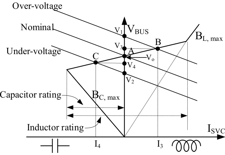
reactive power generation/absorption capability with no power loss during its operation. Figure 2.11a shows an ideal SVC connected to a power bus and Figure 2.11b shows the V/I characteristics of an ideal SVC which is plotted on a graph of AC bus voltage (VBU S) against the SVC reactive current (ISVC). The currentISVC can either be capacitive or inductive depending on the requirement to regulate the bus voltage. If theVBU S is higher
than reference voltageVo, then an inductive current is provided by the SVC to regulate the bus voltage toVo. Similarly, if theVBU Sis lower than theVo then SVC provides capacitive current.
V
BUSI
SVCC
L
(a)Infinite variable reactive power generator.
VBUS
ISVC
Capacitive Region
Inductive Region VO Ideal V/I
characteristic
(b) V/I characteristics of an ideal Static VAR
Compensator.
Figure 2.11: An ideal Static VAR Compensator.
V
BUSI
SVCV
OSlope X
SB
C, maxB
L, maxCapacitor rating
Inductor rating
Figure 2.12: V/I characteristics of an SVC having a fixed capacitor and variable reactor.
SVC provides capacitive current to regulate bus voltage, when the voltage level is lower thanVo. The figure also shows the susceptance limitsBfor the SVC. The V/I characteristics of SVC can be described by the following equations,
VBU S=
Vo+jXs.ISVC when the SVC is the voltage regulation mode
−j ISVC
Bc,max when the SVC is fully capacitive j ISVC
BL,max when the SVC is fully inductive
(2.8)
2.5.1 SVC Characteristics in a Power System
The combined characteristics of an SVC connected to the power system is shown in Fig-ure 2.13. The middle line in the figFig-ure shows the nominal system conditions. During nominal conditions, the bus voltage is equal toVoand the SVC is operating at A, i.e., there
is no current injected or absorbed by the SVC to maintain the bus voltage. When the system voltage increases, due to light loading conditions, the bus voltage increases fromVotoV1
without an SVC. With the SVC, the SVC operating point moves to point B, where it absorbs an inductive currentI3, and moves the system voltage toV3, lower thanV1. Similarly, if the bus voltage decreases fromVo toV2 due to heavy loading conditions, the SVC operating point moves to point C, where it generates a capacitive currentI4, and brings the operating point voltage toV4instead ofV2. As shown in the ideal SVC characteristic in Figure 2.11,
if the slope of SVC characteristic is zero, the bus voltage would have been maintained at
V
BUSI
SVCB
C, maxB
L, maxCapacitor rating
Inductor rating
Nominal
B
Under-voltage
Over-voltage
I3
V1
C
A
V2
V4
V3
I4
Vo
Figure 2.13: V/I characteristics of an SVC having a fixed capacitor and variable reactor with operating points for given power systems.
2.6
Thyristor-controlled reactor (TCR)
SCR1
SCR2
TCR
AC
Mains (HV)
AC
Mains (LV)
Figure 2.14:Thyristor-Controlled Reactor (TCR).
2.6.1 Principle of operation
Each thyristor in the valve conducts on alternate half-cycles of the supply frequency, de-pending on the firing angle α, which is measured from a zero-crossing of the supply voltage. The maximum current contribution is obtained when the forward thyristor, SCR2, is fired at an angle ofπ/2 and the reverse thyristor, SCR1, is fired at 3π/2 as shown in the first plot of Figure 2.15. Partial current contribution is obtained when the firing angleα is varied between π/2 and π for SCR2 (and α+π for SCR1). The firing angles between 0 andπ/2 are not allowed, as they produce asymmetrical current with a DC component. The second plot and third plot in Figure 2.15 show the case when the firing angle is greater than
π2 π/2 π/2 π π π
3π/2
3π/2
3π/2
2π
2π
2π
Firing Angle (α)
Continuous Conduction Partial Conduction Minimum Conduction V V V I I I
Figure 2.15:Voltage and current waveforms in a TCR for different thyristor gating angles.
σ=2(π−α) (2.9)
The instantaneous currenti(t)through a TCR is given by,
i(t) =
√ 2V
XL (cosα−cosωt) forα <ωt<α+σ
0 forα+σ <ωt<α+π
(2.10)
Ldi
dt =vs(t) (2.11)
where Lis the inductance of the reactor in TCR and vs(t) =√2Vsinωt. Integrating the above equation gives,
i(t) =− V
ωLcosωt+C (2.12)
whereC is the constant of integration which can be found by using a boundary condition whenωt=α. Then,
i(ωt=α) =0 (2.13)
Therefore, the instantaneous currenti(t)can be found as,
i(t) = √
2V XL
(cosα−cosωt) (2.14)
2.6.2 Harmonic Analysis for TCR Current
A Fourier analysis is used to calculate the fundamental component of the TCR current
i1(t,α). The Fourier series for the fundamental component of any signal is given as,
i1(t,α) =a1cosωt+b1sinωt (2.15)
It can be seen that the TCR current i(t) in Figure 2.15 has a quarter-wave symmetry. Therefore, the fundamental component of current waveform i1(t,α) has even-function symmetry, i.e., f(−t) = f(t) for all t, therefore b1 =0 and half-wave symmetry, i.e.,
a1can be found as,
a1= 8
T Z T/4
0
f(t)cosωt dt= 4 π
Z π/2 0
f(θ)cosθdθ (2.16)
Solving the integral in Equation (2.16) from firing angleα toπ by using Equation (2.14) gives the following expression of the fundamental component of the thyristor current,
I1(α) = V ωL
2π−2α+sin 2α π
(2.17)
In terms of the conduction angleσ, the fundamental component of the TCR current is given as,
I1(σ) = V ωL
σ−sinσ π
(2.18)
The current can also be written in terms of susceptanceBas,
I1(σ) =V BTCR(σ) (2.19)
where
BTCR(σ) =Bmax
σ−sinσ π
(2.20)
and
Bmax= 1
ωL
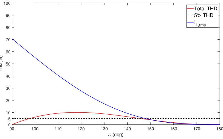
Figure 2.16 shows the variation of the per unit value of BTCR with the firing angleα. As susceptance is the measure of how much a circuit is susceptible to conducting current, the plot in Figure 2.16 shows that the ability to conduct current by the TCR decreases as the firing angle α increases. In other words, a thyristor-controlled reactor acts as variable susceptance (or variable reactance) device. The variation of susceptance changes the fundamental current component which leads to a variable reactor power absorbed by the reactor.
90 100 110 120 130 140 150 160 170 180
(deg)
0 0.1 0.2 0.3 0.4 0.5 0.6 0.7 0.8 0.9 1
XL BTCR
Figure 2.16: Variation of the TCR susceptanceBTCR with firing angleα.
Fourier series as follows,
In= 4
π
Z π/2 0
f(θ)sinθdθ =− V ωL
4 π
Z π α
(cosα−cosθ)cosnθdθ (2.22)
The above equation can be separated into two integrals such as,
In=− V
ωL 4 π
Z π α
(cosαcosnθdθ−cosθcosnθdθ) (2.23)
Using trigonometric identities, the nth-order harmonics are expressed as,
In(α) =− V ωL
4 π
hcosαsinnα
n −
sin(n−1)α 2(n−1) −
sin(n+1)α 2(n+1)
i
= V
ωL 4 π
hsinαcos(nα)−ncosαsin(nα) n(n2−1)
i (2.24)
where n=3,5,7, .... Figure 2.17 shows the variation of the amplitude of different har-monics in the TCR current. It can be seen that the harhar-monics do not peak at the same firing angle. The peak values for different harmonic currents are also expressed as the percentage of the fundamental component in Figure 2.17. Figure 2.18 shows the THD in the TCR current at different firing angles. The plot also shows the decay of the fundamental component of the TCR current with the firing angle.
90 100 110 120 130 140 150 160 170 180 (deg)
0 5 10 15
I n
,%I
1
I3,peak = 13.783%
I5,peak = 5.045%
I7,peak = 2.586%
I9,peak = 1.567%
I11,peak = 1.050%
I13,peak = 0.752%
I15,peak = 0.565%
I17,peak = 0.440%
Figure 2.17: Harmonics in the TCR current.
2.6.3 Three-Phase Thyristor-Controlled Reactor
A three-phase TCR consists of three single-phase TCRs connected in a delta configura-tion. Each leg of a three-phase TCR consists of a reactor connected with two anti-parallel thyristors, therefore requiring a total of six gate firing pulses. If the phases in a three-phase TCR consists of identical reactors and are fed from a balanced three-phase voltage supply, then the harmonic currents generate only odd harmonics given that the thyristors are fired symmetrically.
90 100 110 120 130 140 150 160 170 180
(deg)
0 5 10 20 30 40 50 60 70 80 90 100
THD(%)
Total THD 5% THD I1,rms
Figure 2.18: Total Harmonic Distortion (THD) for the TCR current.
A
B
C
i
CAconnection andIA,IBandICrepresent the line currents in the respective lines connected to the 3-phase delta connection. The nth-order harmonic currents are expressed as,
iAB,n=ancos(nωt+φn) iBC,n=ancos(nωt+φn−n
2π 3 )
iCA,n=ancos(nωt+φn+n
2π
3 ) (2.25)
For triplen-harmonics currents, n=3k+3 and k=0,2, . . .. The nth-order harmonic line currentiA,ncan be calculated as follows,
iA,n=iAB,n−iCA,n=0 (2.26)
Similarly,iB,nandiC,ncan also be calculated. For triplen-harmonic components of the TCR current, the line currentsiA,(3k+3),iB,(3k+3)andiC,(3k+3)reduce to zero. Therefore, the third and multiple of third harmonics generated as a result of the non-sinusoidal TCR current is trapped in the delta configuration and cannot flow into the lines due to balanced operation.
sequence with respect to the peak of that voltage. The control system responsible for the PLL must be fast enough to respond during system faults and voltage fluctuations. The use of a synchronization block for producing gate signals not only poses technical difficulties but also increases the total components required for building a single-phase SVC.
2.7
Thyristor-Switched Reactor (TSR)
The thyristor-switched reactor (TSR) is a special case for the TCR. If the thyristors valves in the TCR are fired at the instants when the voltage peak occurs in the positive and negative half-cycles, it results in the full conduction of TCR current, as shown in Figure 2.15. Therefore, for α =π/2 for positive and α =π in negative half-cycles; maximum current flows in the TCR. However, if no firing pulses are applied, then no current flows through the TCR. The thyristor-switched reactor operates in the same manner as a TCR. However, instead of using two anti-parallel thyristor switches, the TSR uses a single thyristor switch. A major drawback of using the TSR is that instead of getting a variable reactive power as in the case of the TCR, the TSR operates in two states only, i.e., it is either fully on or fully off.
When a large magnitude of inductive reactive power, QL, is required, a part of it is supplied by the TSR, QL,T SR, and the rest is supplied by the TCR, QL,TCR(α). The total inductive reactive power for an SVC arrangement involving a TSR and TCR is given as,
QL=QL,T SR+QL,TCR(α) (2.27)
2.8
Thyristor-Switched Capacitor (TSC)
A thyristor-switched capacitor (TSC) consists of a capacitor bank, which is switched using a thyristor valve. A typical TSC consists of a capacitorC in series with a bi-directional thyristor valve and a small inductor L. The inductor L is used to limit the switching transients and to prevent resonance with the power network.
2.8.1 Principle of Operation
In order to avoid capacitor switching transients, the thyristors are switched when the voltage across them is at a maximum. Therefore, the thyristor firing control system is designed such that the thyristors are fired at the positive or negative peak of the supply voltage. Figure 2.20 shows the operating principle of the switching operation of a TSC. The thyristors are fired at time instant t1, which is chosen such that the bus voltageV is equal to the capacitor
voltageVc in terms of magnitude and polarity. When it is required to open the capacitor
bank, the capacitor banks are switched out at the zero-crossing of the capacitor currentIc,
i.e., when theV =Vc.
2.8.2 Dynamic Response with Multiple TSCs
A thyristor-switched capacitor, in its simplest configuration, consists of a single capaci-tor bank. The size of the capacicapaci-tor bank can be calculated based on the reactive power requirementsQC as,
Creq= V2
ωQC
t
1t
2Bus Voltage
Capacitor Voltage
Capacitor Current
Time
Figure 2.20: Switching operation of a TSC.
where ω is the frequency of the supply voltage. However, instead of using a single ca-pacitor bank, multiple TSC branches can be used. An SVC can have n different values for capacitors on different TSC branches. In this way, there are 2ndiscrete compensation levels, including the zero reactive power level, when all TSC branches are disconnected.
V
BUSI
CS1
S2
C1
A
C
C2
C3
B D
Vref
Figure 2.21 shows the V/I characteristics of an SVC having three TSC branches. The voltage regulation provided by such an SVC is discontinuous or step-wise. In the figure,S1
andS2 represent the power system characteristics. At a certain instant of time, the power system is operating so that its characteristic is represented by line S1 and the voltage of the bus is at point A. At this operating point, capacitor C1is turned on to provide reactive
power support and the bus voltage increases to point B. After a certain time, the system characteristics changes fromS1toS2and the power system is now operating at point C. In
this case, the capacitor bank C2will turn on and change the operating point to D, as shown
in the figure.
Despite the simple construction and working principle of the TSC, it is not widely adopted due to the following disadvantages
• the reactive power compensation provided is not continuous and compensation can only happen in discrete steps,
• each TSC branch in an SVC requires a separate thyristor valve and therefore it is not economical,
• the voltage across the non-conducting thyristor in the thyristor valve is twice as high as the peak supply voltage and thus requires high power rated thyristors.
![Figure 1.1: Average annual growth rates of the world renewables supply from 1990 to2016 [1].](https://thumb-us.123doks.com/thumbv2/123dok_us/1141632.1615876/25.612.125.525.185.437/figure-average-annual-growth-rates-world-renewables-supply.webp)
![Figure 1.2: One-day wind power profile plotted with 1-minute average [4].](https://thumb-us.123doks.com/thumbv2/123dok_us/1141632.1615876/26.612.129.521.284.503/figure-day-wind-power-prole-plotted-minute-average.webp)

![Figure 1.4: ANSI C84.1 standard voltage levels [7].](https://thumb-us.123doks.com/thumbv2/123dok_us/1141632.1615876/28.612.167.487.100.344/figure-ansi-c-standard-voltage-levels.webp)