Abstract—This work defines a novel problem in which a set of modules is assigned to a set of silicon layers in order to minimize the total chip area while satisfying the characteristic constraints. An integer linear programming (ILP)-based partitioning approach is also developed to assign a set of modules to the layers of a three-dimensional architecture during a floor-planning phase. The proposed approach attempts to minimize the chip area, which is the maximum silicon layer area among the set of layers in a three-dimensional system-in-package (SIP) architecture. Moreover, the circuit properties in which the digital and analog modules not to assign to the same layer are incorporated to increase signal integrity during the partitioning stage. The optimal module assignment for the three-dimensional SIP architecture could be obtained because all the constraints in this work are linear functions. Experimental results indicate that the proposed ILP-based method can minimize the chip area while meeting the SIP constraints of circuit properties to reduce the potential interference of the wires in the digital and analog modules. The chip area is larger than that of the method that does not consider interference properties of modules. Importantly, the proposed ILP-based approach significantly reduces the number of the potential interference to be zero by assigning analog and digital modules to the different layers of the SIP architecture.
Keywords—Interference, SIP-ware partitioning, integer linear programming, area minimization.
I. INTRODUCTION
hree-dimensional architecture in modern chip design has many benefits [1][2][3]. The novel three-dimensional SIP architecture can significantly improve the chip area, total wire-length, the number of via count and performance. Hence, an increasing number of studies have investigated how to minimize the chip area for a three-dimensional floor-planner. Moreover, compared to a single-objective, an effective algorithm has been used to solve a multi-objective problem [4].
Manuscript received July 16, 2011: Revised version received August 13, 2011. This work was supported in part by the NSC99-2511-E-262-027 from National Science Council.
Hsin-Hsiung Huang is with the Lunghwa University of Science and Technology, Dept. of Electronic Engineering, No.300, Sec.1,Wanshou Rd., Guishan Shiang, Taoyuan County 33306, Taiwan (R.O.C) (phone:+886-2-82093211ext:5632, fax: +886-2-82095165, e-mail: [email protected])
Tsai-Ming Hsieh is with the Department of Information and Computer Engineering, Chung Yuan Christian University, Chung-Li, 32023, Taiwan (R.O.C.). (corresponding author to provide phone:+886-3-2654708, fax: +886-3-2654799, e-mail: [email protected])
Interference degrades the signal integrity between modules and interconnections with the different properties or circuit characteristics of mixed-mode systems [5]. Tummala derived a solution for a mixed-signal system to meet the emergency requirements [6]. Laas et al. analyzed stochastic parametric resonance and discussed the importance of noise [7]. Drinovsky et al. explored the insertion loss of filter for the EMI effects under a testing environment [8]. Ho et al. discussed the crosstalk (interference) between wires for a multiple-level router [9]. Wang et al. developed a crosstalk aware global router to avoiding assign long segments to different tracks [10]. Most of studies reduce the crosstalk or interference between wire signals by the heuristic algorithms.
The feasibility of applying integer linear programming- based approaches to optimize the chip area, total wire length, power consumption and clock period has been studied. Lin et al.
developed an ILP-based approach to reduce the total wiring area for analog circuit design [11]. Nguyen et al. presented an ILP-based method, which optimizes simultaneously power and delay for the VLSI circuit designs [12]. Chien et al. explored the feasibility of using an ILP-based approach to reduce the power consumption of a gate level netlist under timing, power and area constraints [13]. Chai et al. studied ILP formulations and solved different minimization problems of the peak current and leakage [14]. Huang et al. minimized the clock period for sequential circuit during the high level synthesis using an ILP-based approach [15]. However, most of the above works did not focus on the area minimization for the SIP architecture. Recent efforts have examined the use of novel three-dimensional (3D) floorplanning as the gate counts are growing rapidly [16]. Yamazaki et al. developed the three-dimensional representation of the floorplanners with the multiple objectives such as thermal issues and the area minimization [17]. Hung et al. presented a floorplanner, which considered the thermal issue by incorporating a half-perimeter length estimator [18]. Tsai et al. addressed the thermal issues for the three-dimensional floorplanning with through-silicon- via and the physical position for subcircuits [19]. Xiao et al.
provided the fixed-outline constraints for the three-dimensional floorplanning and inserting through-silicon-via to reduce the incidence of thermal problems [20]. Some of works failed to achieve their objectives when using the heuristic method.
3D Partitioning for Interference and Area
Minimization
Hsin-Hsiung Huang and Tsai-Ming Hsieh
The main contributions of this paper are as follows. This work formulates a module assignment problem which determines the set of modules to the proper layer in a three-dimensional architecture. Circuit properties are formulated to reduce the interference between the analog and digital modules by the ILP formulations. Additionally, all constraints are defined by linearly functions to obtain the optimal solution under the given constraints of the properties. Furthermore, the ILP formulations are efficient to obtain the optimal solution with an acceptable runtime. For each silicon layer, the partitioned results containing some modules can be further fed into a simulated annealing-based floorplanner that applies a sequence-pair to perturb relationships between modules, for a situation in which a feasible floorplan is needed for a three-dimensional architecture.
The rest of this paper is organized as follows. Section II describes the SIP architecture, the number of potential interference, the motivation of consideration of module characteristics and problem definition. Section III then introduces the interference-aware partitioning scheme to minimize the chip area for a three-dimensional architecture. Section IV summarizes the experimental results. Conclusions are finally drawn in Section V.
II. PRELIMINARY
This section describes in detail the system-in-package architecture. The number of potential interference is defined. The motivation of considering the circuit properties is then discussed to explore how the ILP-based approach handles the interference-aware partitioning scheme. Moreover, an interference-aware problem is formulated in the paper.
A. Reviewer and Transformation of System-in-Package
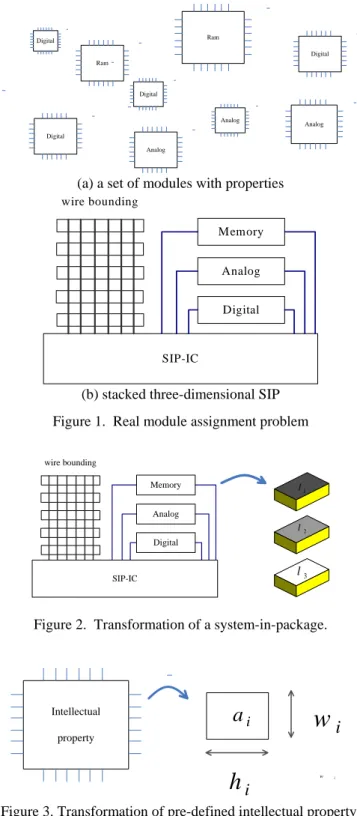
Some approaches have been developed to increase production capacity and reduce time-to-market delivery [1][2][3]. System-in-packet is an effective approach for a three-dimensional architecture [2]. The system-in-packet architecture contains layers, such as the memory (RAM) layers, digital logic layers and analog layers. Figure 1(a) shows a set of pre-defined intellectual properties (IPs for short) which are placed in the corresponding layers of the SIP architecture. Figure 1(b) denotes SIP components, including three layers (i.e. memory, digital and analog layers) and the wire binding, which are used to connect the wires of modules that are located in the different layers.
For simplicity, the SIP architecture is transformed into a set of silicon layers without the wire bounding component. In this work does not consider the interconnections between the different modules in different layers. Figure 2 shows the transformation by omitting the wire binding component and system-in-package integrated circuit (SIP-IC). The three layers are the memory, analog and digital layers. Each module i is transformed into a rectangular module with the corresponding module area (ai), height (hi) and width (wi). Figure 3 illustrates the transformation from an IP into a rectangular module.
Based on the above discussion, Figure 4 plots the problem of assigning IPs to the stacked SIP architecture. Figure 4(a) shows the original circuit which contains six hard modules with the corresponding module areas and the SIP architecture with memory, analog and digital layers. Figure 4(b) shows the representation with six rectangular obstacles and three layers. Moreover, their module properties (i.e. memory, digital or analog) are denoting using three colors.
Ram Ram Analog Analog Analog Digital Digital Digital Digital
(a) a set of modules with properties
Memory
SIP-IC
Analog Digital wire bounding
(b) stacked three-dimensional SIP Figure 1. Real module assignment problem
Memory SIP-IC Analog Digital wire bounding 1 l 2 l 3 l
Figure 2. Transformation of a system-in-package.
Intellectual property i
a
i wi
h
i
w
memory Analog Analog memory Digital Digital Memory SIP-IC Analog Digital wire bounding ` (a) 6 modules
a
2 = 2a
4 = 4a
3= 3a
5 = 5a
1 = 1a
6 = 6 analgo memory digital 1l
2l
3l
(b) 3D architectureFigure 4. Illustration of the SIP-aware 3D partitioning
B. Computation of the Number of Potential Interference
Signal integrity plays a significant role in the modern chip designs because of the increasing number of the digital and analog modes co-designed in a single system.
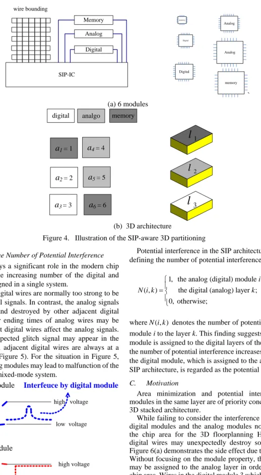
As is well known digital wires are normally too strong to be high level or low level signals. In contrast, the analog signals are easily degraded and destroyed by other adjacent digital wires. The starting or ending times of analog wires may be delayed when adjacent digital wires affect the analog signals. Furthermore, an unexpected glitch signal may appear in the analog modules when adjacent digital wires are always at a high or low voltage (Figure 5). For the situation in Figure 5, properties of the analog modules may lead to malfunction of the analog signals in the mixed-mode system.
Interfeuce by digital module high voltage
low voltage
high voltage
low voltage
wires in digital module wires in analog module
Figure 5. Illustration of the potential interference
Potential interference in the SIP architecture is measured by defining the number of potential interference as follows.
1, the analog (digital) module is assigned to ( , ) the digital (analog) layer ;
0, otherwise; i N i k k ⎧ ⎪ = ⎨ ⎪ ⎩ (1)
whereN i k( , ) denotes the number of potential interference for module i to the layer k. This finding suggests that if the analog module is assigned to the digital layers of the SIP architecture, the number of potential interference increases by one. Similarly, the digital module, which is assigned to the analog layer in the SIP architecture, is regarded as the potential interference.
C. Motivation
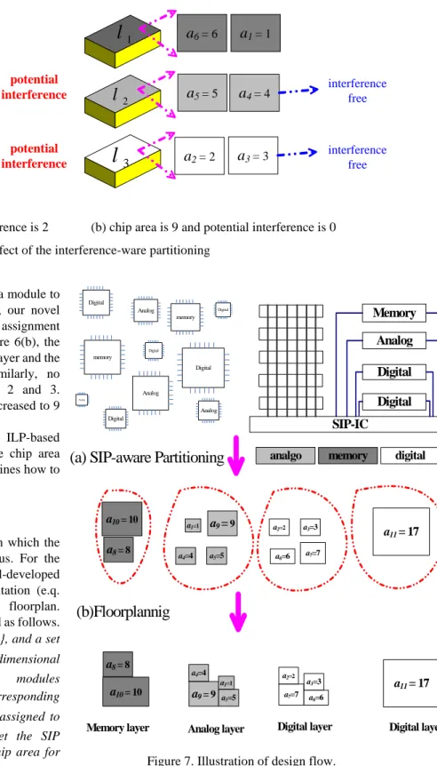
Area minimization and potential interference between modules in the same layer are of priority concern in the modern 3D stacked architecture.
While failing to consider the interference issue between the digital modules and the analog modules normally minimizes the chip area for the 3D floorplanning However, adjacent digital wires may unexpectedly destroy some analog wires. Figure 6(a) demonstrates the side effect due to the interference. Without focusing on the module property, the digital modules may be assigned to the analog layer in order to minimize the chip area. Wires in the digital module 3 which is assigned to the analog layer potentially degrade the wires in the analog module 4. Similarly, the wires in the analog module 5 may suffer under the same circumstances.
a
6 = 6a
1= 1a
4= 4a
3 = 3a
2 = 2a
5= 5 potential interference potential interference 1l
2l
3l
a
6 = 6a
1 = 1a
4 = 4a
3 = 3a
2 = 2a
5 = 5 interference free interference free 1l
2l
3l
(a) chip area is 7 and potential interference is 2 (b) chip area is 9 and potential interference is 0 Figure 6. Effect of the interference-ware partitioning
While considering the SIP constraints to assign a module to the corresponding layers in the SIP architecture, our novel formulations obtain the interference-free module assignment solution with a little additional chip area. In Figure 6(b), the analog modules 4 and 5 are assigned to the analog layer and the number of potential interferences is zero. Similarly, no potential interference occurs for digital layers 2 and 3. According to our results, the chip area could be increased to 9 with small additional chip area.
This observation motivates us to explore the ILP-based SIP-aware formulations in order to minimize the chip area while meeting the SIP constraints. This work examines how to achieve this multiple-objective in this paper.
D. Problem Definition
Figure 7 shows the overall 3D floorplanning, in which the SIP-aware partitioning stage is of particular focus. For the partitioned results in each layer, the well-developed floorplanner which is based on the 2D representation (e.q. sequential-pair) can used to obtain a feasible floorplan. Therefore, the problem discussed here is formulated as follows.
Given a set of n module area {a1, a2, a3, . . . a }, and a set n of k silicon layers { l1, , , . . . l2 l3 lk} for three-dimensional
SIP architecture. For a set of n modules
{ m1, m2, m3, . . . mn } , each module has it corresponding
properties {p1, p2, p3, . . . ,p }. Each module is assigned to n one silicon layers. The work attempts to meet the SIP characteristic constraints while minimizing the chip area for the SIP architecture.
memory Analog Analog Digital memory Analog Analog Digital Digital Digital Digital
(a) SIP-aware Partitioning
(b)Floorplannig
a4=4 a5=5 a2=2 a7=7 a1=1 a11 = 17 a9 = 9 a3=3 a6=6 a8 = 8 a10 = 10analgo memory digital
Memory SIP-IC Analog Digital Digital a8 = 8 a10 = 10 a11 = 17 a9 = 9 a5=5 a4=4 a1=1 a7=7 a6=6 a2=2 a3=3
Memory layer Analog layer Digital layer Digital layer
memory Analog Analog Digital memory Analog Analog Digital Digital Digital Digital Memory SIP-IC Analog Digital wire bounding Digital ` analgo memory digital a8 = 8 a10 = 10 a4 = 4 a1= 1 a5 = 5 a9 = 9 a2 = 2 a3 = 3 a6 =6 a7 = 7 a11 = 17 1
l
2 l 3l
4l
(a) 3D SIP partitioning (b) ModelingFigure 8. Illustration of interference-free three-dimensional partitioning
III. ILP FORMULATION FOR SIP-AWARE PARTITIONING This section discusses ILP formulations with interference-aware for the SIP architecture, in which the module shaped is fixed (i.e. hard modules). Many floorplanners have been developed in the recent literature. Therefore, this work discusses in detail the SIP-aware partitioning.
A. Area Minimization Formulation with SIP constraints
An attempt is made to determine automatically the module assignment automatically by setting a binary variable
x i j
( , )
to one, if the module
i
is assigned to the layerj, otherwise( , )
x i j
is set to be zero. The objective of this work is derived as follows,min total_area (2)
Subject to
= 1 den otes allow ed layers
( , )
1;
n i jx i j
=
∑
∑
(3) 1 total_area ( , ); n i i a x i j = ≥∑
× (4) where ( , )x i j denotes the binary variable for the modulei
, which is assigned to the layerj
. airepresents the module area of the modulei
. For each module, to meet the SIP constraints, not all layers in a three-dimensional SIP architecture could be assigned. The total_arearefers to the maximum chip area among the three-dimensional SIP architecture with klayers. Formula (2) gives the objective to minimize the chip area for the three-dimensional SIP architecture withklayers. Formula (3) indicates that each modulei
is assigned to only one layerj
. Formula (4) reveals that the maximum chip area is larger than the area of each layerj
. By doing so, the number representing the layer area can be reduced. Originally, the area of each layer is denoted by using four variables. Notably, reducing four variables into one variable speeds up the computational time.Reducing the potential interference for the analog modules and digital modules involves the module assignment according to the module property and the SIP-aware constraints. This finding suggests that the binary values denoting the module assignment should be modified. For instance, if module 1 is the analog module and this module should be assigned to layer 2 in order to reduce the potential interference for the SIP architecture with four layers, the binary variable should be
(1, 2) 1
x = and x(1,1) = x(1,3) = x(1,4) = 0 .
B. Illustrative Example
By using an illustrative example, this subsection explains how to formulate the proposed ILP formulations with a SIP constraint. Originally formulated as Figure 8(a), Figure 8(b) shows four layers and 11 modules with the corresponding properties. For the SIP-aware partitioning scheme, n=11and
4
k= . Similarly, the objective is described as follows. min = total_area; (5) Figure 8(b) reveals the following constraints to represent the chip area. 1 2 3 4 5 6 7 8 9 10 11 1; 2; 3; 4; 5; 6; 7; 8; 9; 10; 17; a a a a a a a a a a a = = = = = = = = = = = (6)
Notably, in this paper, no module is partitioned and we the module assignment is defined by using the binary variable. For module 1, four options are available to place in a three-dimensional SIP architecture, thus leading to
(1,1)x +x(1, 2)+x(1, 3)+x(1, 4)=1; (7) To meet paper space limitation, only modules 2and 11 are used to represent the relation as follows.
(2,1)x +x(2, 2)+x(2,3)+x(2, 4)=1; (8) and
a8= 8 a10 = 10 a4= 4 a5= 5 a2= 2 a7= 7 a1= 1 a11= 17 a9= 9 a3= 3 a6= 6 potential interference potential interference potential interference 1 l 2 l 3 l 4 l a8= 8 a10= 10 a4= 4 a5 = 5 a2= 2 a7= 7 a1 = 1 a11= 17 a9= 9 a3= 3 a6= 6 Interference free 1 l 2 l 3 l 4 l
(a) partitioning with potential interference (b) interference-free partitioning Figure 9. Illustration of interference-free SIP partitioning
The area bound for all layers containing a set of modules is given. In layer 1, the total layer area is the sum of module areas from modules 1 to 11. Based on the above discussion, we define binary variables (1,1)x , (2,1)x , . . ., and (11,1)x to denote the relation of all modules and all layers, respectively. The layer area in layer 1 is obtained with the following formula.
1 2 3 4 5 6 7 8 9 10 11 total_area (1,1) (2,1) (3,1) (4,1) (5,1) (6,1) (7,1) (8,1) (9,1) (10,1) (11,1); a x a x a x a x a x a x a x a x a x a x a x ≥ × + × + × + × + × + × + × + × + × + × + × (10)
Similarly, the layer area can be formulated based on the above discussion for layers 2, 3 and 4.
Without considering SIP constraints (circuit properties) of modules and layers in the SIP architecture, the assigned module can be derived as follows.
(8,1) (10,1) 1 x =x = (11) (2, 2) (4, 2) (5, 2) (7, 2) 1 x =x =x =x = (12) (1,3) (11, 3) 1 x =x = (13) and (3, 4) (6, 4) (9, 4) 1 x =x =x = (14) The above equations reveal that the optimal chip area is
_ 18
total area= with potential interference. Figure 9(a)
summarizes the partitioned results for this circuit. In layer 2 (an analog layer), digital modules 2 and 7 are assigned. According to the computation of the potential interference, the number of potential interference is 2. Similarly, analog modules 1 and 9 are assigned to the layers 3 and 4 (two digital layers) and the number of the potential interference is 1 and 1, respectively. Therefore, the approach without considering the potential interference between the modules, the number of potential interference is 4. The interference of module assignment must be addressed and reduced.
Considering the SIP constraints which are based on the
properties of the modules and the layers allows us to reduce the potential interference issue. For module 2, it is proper to assign
this module to the digital layers 3 and 4 and we have the formula of x(2,3)+ x(2,4)=1. Similarly, for module 3, we have
x(3,3)+ x(3,4)=1. For the digital modules 6, 7 and 11, we have
x(6,3)+ x(6,4)=1, x(7,3)+ x(7,4)=1 and x(11,3)+ x(11,4)=1. Involving the above constraints in the LIP formulation allows us to minimize the chip area while reducing the number of potential interference. The module assignment is as follows.
(8,1)x =x(10,1)=1 (15) (1, 2) (4, 2) (5, 2) (9, 2) 1 x =x =x =x = (16) (2, 3) (3, 3) (6, 3) (7, 3) 1 x =x =x =x = (17) and (11, 4) 1 x = (18) According to our results, the chip area is increased to 19 (total_area=19). Formulas (15)-(18) indicate that modules 8 and 10 are assigned to layer 1; modules 1, 4, 5 and 9 are assigned to layer 2; modules 2, 3, 6 and 7 are assigned to layer 3; and module 11 is assigned to layer 4. Figure 9(b) reveals that the analog modules 1, 4, 5 and 9 are assigned to the analog layers in order to avoid potential interference. Similarly, the number of potential interferences of layers 3 and 4 are reduced to zero by involving SIP constraints.
Summary, the chip area is increased only slightly (from 18 to 19) while reducing the number of potential interference (from 4 to 0). This finding suggests that the proposed SIP-aware partitioning approach can simultaneously minimize the chip area and the potential interference for the signals between the digital and analog modules.
IV.EXPERIMENTAL RESULTS
In this work, ILP formulations are generated automatically by C++ language, along with experiments performed on an Intel 2.40GB machine with 1GB memory in order to optimize the chip area for a 3D stacked SIP architecture with four metal layers. Effectiveness of the proposed ILP formulations is demonstrated by using GRSC benchmarks that are utilized to perform experiments. Table 1 lists the statistics of GRSC benchmarks, including the circuit name, the number of modules, the module area, the chip area and percentage of area reduction.
First, effectiveness of the ILP-based approach is examined. Compared with the theoretically results, i.e. total module area based on the number of layer, the ILP-based approach without SIP minimizes the chip area. Tables 1 and 2 show that both the ILP-based without and with SIP constraint reduce the chip area. With an acceptable runtime, the partitioned results are obtained efficiently.
Additionally, the improvement in the number of the potential interference is also examined. In the formulations with SIP consideration, the digital and analog modules are placed in the different layers. Hence, the signals in analog modules did not be affected by interconnects in the digital modules. According to Table 3, the number of potential interference is reduced to zero.
V. CONCLUSIONS
This work defines a novel problem of a 3D SIP-aware partitioning scheme and solves it by using the ILP-based approach. The objective is to minimize the chip area while satisfying the SIP constraints in order to reduce the potential interference. All constraints are linear to formulate this SIP-aware partitioning problem. Experimental results indicate that the proposed ILP-based SIP-aware method reduce the area compared to the total module area. Furthermore, the SIP-aware approach more significantly reduces the number of potential interferences than with partitioning approach without the SIP constraints.
ACKNOWLEDGEMENTS
The authors would like to thank the financial support of the grant NSC99-2511-E-262-027 from National Science Council.
REFERENCES
[1] J. Minz, and S.K. Lim, "Block-level 3D Global Routing With an Application to 3D Packaging," IEEE Transactions on Computer-Aided
Design of Integrated Circuits and Systems, Vol. 25, No. 10, pp.
2248-2257, 2006.
[2] Jiwoo Pak; Myunghyun Ha; Jaemin Kim; Donghee Kang; Ho Choi; Seyoung Kwon; Keunsoo La; Joungho Kim, “Design of a 3-D SiP for T-DMB with Improvement of Sensitivity and Noise Isolation,” in Proc.
of Electronics Packaging Technology Conference, pp.1387-1392, 2008.
[3] S. K. Lim, “Physical design for 3D System-on-Package,” IEEE Des. Test.
Comput., vol. 22, no. 6, pp. 532–539, 2005.
[4] Anon Sukstrienwong, “Solving Multiobjective Optimization under Bounds by Genetic Algorithms,” International Journal of Computers, pp. 18-25, 2011.
[5] Luis F. C. Duarte, Jose D. Zambianco, Douglas Airoldi, Elnatan C. Ferreira and Jose A. Siqueira Dias, “Characterization and Breakdown of the Electricity Bill using Custom Smart Meters: a Tool for Energy-Efficiency Programs,”, International Journal of Circuits,
Systems and Signal Processing, pp.116-123, 2011.
[6] R. Tummala, “SOP: What is It and Why? A New Microsystem-Integration Technology Paradigm—Moore’s Law for System Integration of Miniaturized Convergent Systems of the Next Decade,” IEEE Trans. Adv. Package., vol. 27, no. 2, pp. 241–249, 2004. [7] Katrin Laas, Romi Mankin, Astrid Rekker, “The Influence of Noise Kurtosis on the Dynamics of a Harmonic Oscillator with Fluctuating
frequency,” International Journal of Mathematical Models and Method in Applied Sciences, pp. 27-36, 2009.
[8] J. Drinovsky, Z. Kejik, V. Ruzek, and J. Zachar, “EMI Filters Worst-case Identification by Alternative Measurement System,” International
Journal of Circuits, Systems and Signal Processing, pp.212-219, 2011.
[9] T.Y. Ho, Y.W. Chang, S.J. Chen, and D.T. Lee, “Crosstalk- and Performance-Driven Multilevel Full-Chip Routing,” IEEE Transaction
on Computer-Aided Design of Integrated Circuits and Systems, Vol. 24,
No. 6, pp. 869-878, 2005.
[10] C.H. Wang, H.H. Huang, Y.C. Chen, C.H. Lee and T.M. Hsieh, “A New Congestion and Crosstalk Aware Router,” Proc. IEEE of International
Symposium on Circuits and Systems, pp. 6234-6237, 2005.
[11] C.C. Lin, H.H. Huang, H.A. Chien, T.M. Hsieh, “Obstacle-Avoiding Electromigration Aware Wire Planning for Analog Circuits” Proc. of
IEEE International Symposium on Integrated Circuits, pp. 651-654,
2009.
[12] D. Nguyen et al. “Minimization of Dynamic and Static Power Through joint Assignment of Threshold Voltages and Sizing Optimization,” Proc.
of ACM International Symposium on Low Power Design, pp. 158-163,
2000.
[13] H.A. Chien, C.C. Lin, H.H. Huang and T.M. Hsieh, “Optimal Supply Voltage Assignment under Timing, Power and Area Constraints,” IEICE Transactions on Fundamentals of Electronics, Communications, and
Computer Sciences, Vol.E93, NO4, pp. 761-768, 2010.
[14] D. Chai and A. Kuehlmann, “Circuit-based Preprocessing of ILP and Its Applications in Leakage Minimization and Power Estimation,” in Proc.
of IEEE/ACM International Conference on Computer Design, pp.1-6,
2004.
[15] S.H. Huang, C.H. Cheng, Y.T. Nieh, and W.C. Yu , “Register Binding for Clock Period Minimization,” Proc. of ACM/IEEE Design
Automation Conference, pp.439-444, 2006.
[16] L. Cheng, L. Deng and D. F. Wong, “Floorplanning for 3D VLSI design,” Proc. of ACM/IEEE Asia-South Pacific Design Automation
Conference, pp.405-411, 2005.
[17] H. Yamazaki, K. Sakanushi, S. Nakatake and Y. Kajitani, “The 3D Packing by Meta Data Structure and Packing Heuristics,” IEICE Trans.
on Fundamentals, pp.639-645, 2000.
[18] W.L. Hung, G.M. Link, X. Yuan, N. Vijaykrishnan, and M.J. Irwin, “Interconnect and Thermal-aware Floorplanning for 3d Microprocessors,” Proc. of International Symposium on Quality
Electronic Design, pp. 6, 2006.
[19] M.C. Tsai, T.C. Wang, and T. T. Hwang, “Through-Silicon Via Planning in 3D Floorplanning,” IEEE Transactions on Very Large Scale
Integration Systems, pp.1-10, 2010.
[20] L. Xiao, S. Sinha, J. Xu, F.Y Young, “Fixed-Outline Thermal-aware 3D Floorplanning,” Proc. of ACM/IEEE Asia and South Pacific Design
Automation Conference, pp.561-567, 2010.
Hsin-Hsiung Huang received the M.S. and Ph.D. degrees in the Dept.
Information Computer Engineering and Electronic Engineering from Chung Yuan Christian University, Taoyuan, Taiwan, in 2000 and 2008, respectively. From 2000 to 2002, He is a hardware engineering to design the Ethernet product at Accton Corporation, Hsin-Chu, Taiwan. From 2002 to 2003, He focus on the chip design for the 10/100/1000 Mbps Ethernet MAC at TM-Technology Corporation, Hsin-Chu, Taiwan. His is interested in the design and analysis of the algorithms. He is working toward the algorithm–related fields, such the application of line-following maze robot and CAD algorithms for the VLSI, the floorplanner and performance-driven routing with the obstacles.
Tsai-Ming Hsieh received his B.S. degree in Electrical Engineering form
Chung Yuan University, Chung-Li, Taiwan, in 1970 and his M.S. and Ph.D degrees in Electrical Engineering from the Institute of Electronics, National Chiao Tung University, Hsinchu, Taiwan, in 1974 and 1983, respectively. He is currently a professor of the Department of Information and Computer Engineering at Chung Yuan University. His current research interests are in computer-aided design on integrated circuits, design and analysis of algorithms, and combinational mathematics.
sTable 1. Benchmark statistics and results without SIP constraints.
Name A
B
C
Imp1
(%)
n10 10 221679
56168 74.66246
n30 30 208591
52150 74.99892
n50 50 198579
49645 74.99987
n100 100 179501
44876
74.99958
A= “number of modules for each benchmark”;
B= “total module area”; and C= “chip area without SIP”;
Imp1(%)= “the reduction of chip area without SIP (=100 ×(B-C)/B)”;
Table 2. Benchmark statistics and results with SIP constraints.
Name A
B
D
Imp2
(%)
n10 10 221679
91347 58.79312
n30 30 208591
54892 73.68439
n50 50 198579
54882 72.36264
n100 100 179501
52026
71.01632
B= “total module area”; D= “chip area with SIP”;
Imp2(%)= “the reduction of chip area with SIP (=100 ×(B-D)/B)”;
Table 3. Comparison of the number of potential interference without and with SIP constraints.
Name A
E
F
Imp3
n10 10
2
0
2
n30 30
10
0
10
n50 50
13
0
13
n100 100
26
0
26
E= “The number of potential interference without SIP”; F= “The number of potential interference with SIP”; Imp3= E-F;