Vom Fachbereich Informatik der Technischen Universität Darmstadt
genehmigte
Dissertation
zur Erlangung des akademischen Grades Doktor Ingenieur (Dr.-Ing.)
vorgelegt von
Nicolas Weber, M.Sc.
geboren in Hanau.Referenten: Prof. Dr.-Ing. Michael Goesele Technische Universität Darmstadt Prof. Dr. Michael Gerndt
Technische Universität München
Tag der Einreichung: 13.04.2017 Tag der Disputation: 19.06.2017
Darmstädter Dissertation, 2017 D 17
Hiermit versichere ich die vorliegende Dissertation selbstständig nur mit den angegeben Quellen und Hilfsmitteln angefertigt zu haben. Alle Stellen, die aus Quellen entnommen wurden, sind als solche kenntlich gemacht. Diese Arbeit hat in gleicher oder ähnlicher Form noch keiner Prüfungsbehörde vorgelegen. Darmstadt, den 13.04.2017
Graphics Processing Units(GPUs)have been used for years in compute intensive applications. Their massive parallel processing capabilities can speedup calcula-tions significantly. However, to leverage this speedup it is necessary to rethink and develop new algorithms that allow parallel processing. These algorithms are only one piece to achieve high performance. Nearly as important as suitable algorithms is the actual implementation and the usage of special hardware features such as intra-warp communication, shared memory, caches, and memory access patterns. Optimizing these factors is usually a time consuming task that requires deep under-standing of the algorithms and the underlying hardware. UnlikeCentral Processing Units(CPUs), the internal structure of GPUs has changed significantly and will likely change even more over the years. Therefore it does not suffice to optimize the code once during the development, but it has to be optimized for each new GPU generation that is released. To efficiently (re-)optimize code towards the underlying hardware, auto-tuning tools have been developed that perform these optimizations automatically, taking this burden from the programmer. In particular, NVIDIA – the leading manufacturer for GPUs today – applied significant changes to the memory hierarchy over the last four hardware generations. This makes the memory hierarchy an attractive objective for an auto-tuner.
In this thesis we introduce the MATOG auto-tuner that automatically optimizes array access for NVIDIA CUDA applications. In order to achieve these optimizations, MATOG has to analyze the application to determine optimal parameter values. The analysis relies on empirical profiling combined with a prediction method and a data post-processing step. This allows to find nearly optimal parameter values in a minimal amount of time. Further, MATOG is able to automatically detect varying application workloads and can apply different optimization parameter settings at runtime. To show MATOG’s capabilities, we evaluated it on a variety of different applications, ranging from simple algorithms up to complex applications on the last four hardware generations, with a total of 14 GPUs. MATOG is able to achieve equal or even better performance than hand-optimized code. Further, it is able to provide performance portability across different GPU types (low-, mid-, high-end and HPC) and generations. In some cases it is able to exceed the performance of hand-crafted code that has been specifically optimized for the tested GPU by dynamically changing data layouts throughout the execution.
Graphics Processing Units(GPUs)werden seit Jahren für berechnungsintensive An-wendungen eingesetzt. Ihre massiv-parallele Rechenleistung kann Berechnungen signifikant beschleunigen. Um diese Beschleunigung zu erreichen ist es notwendig, dass Algorithmen überarbeitet oder neu entwickelt werden, um parallele Berech-nungen zu ermöglichen. Diese Algorithmen jedoch sind nur ein Teil um hohe Berechnungsgeschwindigkeiten zu erreichen. Genauso wichtig wie raffinierte Al-gorithmen, ist die eigentliche Implementierung und die Nutzung von speziellen Komponenten wie Intrawarp Kommunikation, geteilte Speicher, Zwischenspeicher und Speicherzugriffsmuster. Diese Faktoren zu optimieren ist üblicherweise eine zeitintensive Aufgabe, welche ein umfassendes Verständnis der Algorithmen und des Beschleunigers erfordert. Anders als beiCentral Processing Units(CPUs)hat sich die interne Struktur von GPUs in den letzten Jahren stark verändert und wird sich mit Sicherheit weiterentwickeln. Deshalb reicht es nicht aus, Programme nur während der Entwicklung zu optimieren. Um effizient Programme für ein bestimmtes Gerät zu optimieren wurden Auto-Tuner entwickelt, welche diese Optimierungen automatisch durchführen und somit die Programmierer entlasten. NVIDIA – der führende Hersteller von GPUs – hat in letzten vier Generationen signifikante Änderungen an der Speicherhierarchie vorgenommen. Dies macht die Speicherhierarchie zu einem attraktiven Ziel für einen Auto-Tuner.
In dieser Arbeit stellen wir den MATOG Auto-Tuner vor, welcher automatisch Ar-rayzugriffe in NVIDIA CUDA Anwendungen optimiert. Um diese Optimierungen zu erreichen, muss die Anwendung analysiert und optimale Parameter gefunden werden. Diese Analyse basiert auf empirischen Messungen kombiniert mit einer Vorhersagemethode und einer Datennachverarbeitung. Dies erlaubt es nahezu op-timale Parameter in kürzester Zeit zu finden. MATOG ist darüber hinaus in der Lage verschiedene Programmzustände zu erkennen und unterschiedliche Optimierun-gen zur Laufzeit anzuwenden. Um die Fähigkeiten von MATOG zu beleOptimierun-gen haben wir eine Auswahl von simplen und komplexen Anwendungen auf den letzten vier Hardware Generationen mit insgesamt 14 verschiedenen GPUs getestet. MATOG ist in der Lage äquivalente, bzw. teilweise auch bessere Leistung als handopti-mierte Implementierungen zu erreichen. Weiterhin bietet es Leistungsportabilität über verschiedene GPU Typen und Generationen. In einigen Fällen kann MATOG die Leistung von handoptimiertem Code übertreffen, indem es dynamisch die Speicherlayouts zur Laufzeit anpasst.
First of all, I would like to thank my supervisor Michael Goesele for the opportunity to work in his research group for the last four years, his support and valuable feed-back. The work environment he created is challenging and sometimes exhausting but exactly this makes it fruitful and pushes one to seek and achieve even more. It was a pleasure to work with him for all these years.
I would also like to extend my sincere gratitude to Michael Gerndt who kindly agreed to be referee for this thesis.
Next, I would like to give special thanks to my colleagues, starting with Martin Hess. We shared an office for all these years and had many inspiring/funny discussions! One great hug goes to Michael Wächter who never gave up on me and pushed me all the way through the obstacles of theDetail-Preserving Image Downscaling
(DPID)paper [Weber et al. 2016]. Further, I want to thank Dominik Wodniok, not only for all the discussions we had, but also his valuable feedback for MATOG and DPID. A special thanks goes to Sandra C. Amend for her support in all the annoying programming tasks that had to be done.
Finally, I want to thank my parents who always supported me, my brothers and all my friends for their help and support.
The work of Nicolas Weber is supported by the ‘Excellence Initiative’ of the Ger-man Federal and State Governments and the Graduate School of Computational Engineering at Technische Universität Darmstadt.
Frontmatter
Abstract III Zusammenfassung V Acknowledgements VIIMain Content
1 Introduction 1 1.1 Contributions . . . 4 1.2 Thesis Outline . . . 6 2 Background 7 2.1 Computational Basics . . . 7 2.1.1 Processor Architectures . . . 72.1.2 Memory Hierarchy and Caches . . . 8
2.1.3 Multi-Tasking and Scheduling . . . 9
2.1.4 Processing Improvements . . . 10 2.1.5 Multi-Processing . . . 10 2.1.6 Performance Classification . . . 12 2.1.7 Performance Limitations . . . 14 2.2 Hardware Implementations . . . 14 2.2.1 Bus Systems . . . 15 2.2.2 Processor Performance . . . 15
2.2.3 Caches for Parallel Processing . . . 17
2.2.4 Parallel Processors and Accelerators . . . 17
2.2.6 Memory Types . . . 21
2.3 Array Layouts . . . 21
2.3.1 Multidimensional Indexing . . . 21
2.3.2 Struct Layouts . . . 22
3 Target Architecture and Platform 25 3.1 NVIDIA CUDA . . . 25
3.1.1 Compute Model . . . 25
3.1.2 Programming Language . . . 28
3.1.3 CUDA Profiling Tools Interface . . . 30
3.2 NVIDIA GPUs . . . 33
3.2.1 Fermi Architecture . . . 33
3.2.2 Kepler Architecture . . . 33
3.2.3 Maxwell Architecture . . . 34
3.2.4 Pascal Architecture . . . 34
4 Auto-Tuning and Related Work 37 4.1 Options for optimization . . . 39
4.2 How to integrate optimizations into applications? . . . 40
4.3 Which configurations are optimal? . . . 40
4.4 How to detect and handle runtime dependent performance effects? 42 4.5 Overview . . . 42
4.5.1 Performance Measurement, Modeling and Simulation . . . 43
4.5.2 Compilers . . . 44
4.5.3 Programming Languages . . . 45
4.5.4 Domain Dependent Auto-Tuning . . . 46
4.5.5 Domain Independent Auto-Tuning . . . 47
4.5.6 Memory Access and Data Layouts Auto-Tuning. . . 50
5 MATOG Auto-Tuner 53 5.1 Programming Interface . . . 54
5.2 Programming Example . . . 54
5.3 Implementation Details . . . 56
5.3.2 Shared Memory . . . 60
5.3.3 Optimization Hints . . . 61
6 Application Analysis 63 6.1 Optimization Problem . . . 63
6.2 Step 1: Application Profiling . . . 64
6.2.1 In-Application Profiling . . . 64
6.2.2 Prediction Based Profiling . . . 65
6.3 Step 2: Determine Optimal Configurations . . . 68
6.3.1 Decisions . . . 68
6.3.2 Array Dependencies. . . 69
6.3.3 Exhaustive Search. . . 69
6.3.4 Predictive Search . . . 70
6.4 Step 3: Decision Models . . . 71
6.4.1 Directional Model. . . 71
6.5 MATOG Runtime System . . . 72
7 Evaluation 75 7.1 Benchmark Applications . . . 75
7.1.1 Bitonic Sort . . . 76
7.1.2 Speckle Reducing Anisotropic Diffusion . . . 77
7.1.3 Hotspot . . . 78
7.1.4 Detail Preserving Image Downscaling . . . 78
7.1.5 Coevolution via MI on CUDA . . . 79
7.1.6 Renders Everything You Ever Saw . . . 79
7.1.7 KD-Tree. . . 79
7.2 Execution Performance . . . 82
7.2.1 GPU Execution Time . . . 82
7.2.2 Application Execution Time . . . 88
7.2.3 Performance Portability . . . 91
7.2.4 Analysis Time . . . 92
8 Empirical Performance Models 95 8.1 Model Training and Prediction Accuracy . . . 97
8.1.1 Single Dataset . . . 97
8.1.2 Multiple Datasets . . . 100
8.1.3 Error Cases . . . 102
8.2 Predicting Unknown Configuration Performance . . . 105
9 Discussion 107 9.1 Summary . . . 107
9.2 Is auto-tuning useful? . . . 108
9.3 Which optimizations are optimal? . . . 108
9.4 MATOG Implementation Improvements . . . 114
9.5 Conclusion . . . 115
10 Future Work 117 10.1 Future of MATOG . . . 117
10.2 Evaluation and comparability . . . 118
10.2.1 Benchmark Suites. . . 119
10.2.2 Collective Knowledge . . . 120
10.3 How to combine different optimizations? . . . 120
10.4 Performance models, continuous monitoring and adaptive reopti-mization . . . 121
10.5 Incompatibility of Auto-Tuners . . . 121
10.6 Performance Portability Aware Software Stack . . . 122
Appendix
A Benchmark Training-/Testing-Data 125 A.1 Bitonic Sort . . . 125A.2 SRAD . . . 125 A.3 Hotspot . . . 126 A.4 DPID . . . 126 A.5 COMIC . . . 127 A.6 REYES . . . 127 A.7 KD-Tree . . . 128
Acronyms 129
Bibliography 133
Introduction
Writing efficient code is one of the major objectives for programmers, besides the correctness of the calculations. However, efficiency covers multiple factors, such astime,energyandcost. Depending on the application the focus is shifted
between these factors. For example, gaming hardware is tuned to deliver highest performance rather to have a low energy consumption [Mills and Mills 2015]. The costs have to be moderate, so that a private person can afford the computer. Supercomputers also have striven for highest available performance [Top 500 2016] for many years. However, today many supercomputers seek to provide high performance with low energy consumption [Green 500 2016], to keep the costs reasonable. In general, costs consist of the initial expenses for the hardware, maintenance costs, power consumption (which can be several million dollars per year for supercomputers) and costs for developing and optimizing the software. To reduce the costs, on the one hand applications have to be time and energy efficient to optimize the utilization and lower the energy consumption. On the other hand, this increases the costs for development and optimization. Unfortunately, code efficiency always depends on the underlying hardware. It has to be specifically designed for the hardware it is running on. This requires that experts with a deep understanding of both, the hardware and the application, optimize the code, which again increase the costs [Bischof et al. 2012].
The first computers have been executing a single application on a single threaded processor [Goodacre 2011]. With the upcoming of Intel’s x86 architecture, it became the standard architecture for many years [Levenson 2013]. It caused that software was mainly developed for this particular architecture. For years this worked, as technological advances allowed to develop faster processors without changing the architecture significantly. This effect had been predicted byMoore [1965]which became to known as“Moore’s Law”. However, these advances had
stalled and introduced a demise of Moore’s Law [Berkeley 2014] (Section 2.2.2). To further improve the performance of processors, other methods had to be found. One of these is parallel computation. Parallel processors can have up to several thousand compute cores operating in parallel. This parallel processing power comes with the necessity of writing efficient code that enables all cores of the processors to solve a problem together. Therefore, not only algorithms have to be rethought and specifically designed for parallel processing but also the actual implementation has to utilize available hardware features. Today, the market is
filled with all kinds of processors, specifically designed to excel in a particular field. There are all kinds of variations of processors ranging from few, but fast compute cores (multi-core CPUs) to processors with thousands, but rather slow cores (GPUs). Also special purpose processors are available, specifically tuned for a specific purpose, e.g., Google’sTensor Processing Unit(TPU)[Jouppi 2016] that is optimized for neural network processing. This variety of processors poses a challenge to software developers as they no longer have only one dominant architecture their software has to be developed and optimized for. They have to deal with varying processor designs, number of processing cores, specialized hardware functionality, programming languages, library support and operating systems.
Further, hardware architectures (even from the same manufacturer) undergo con-stant changes and improvements, introducing new, changed or removed function-ality. NVIDIA is the leading manufacturer for GPUs today [Shilov 2016]. NVIDIA’s GPUs consist of a complex memory hierarchy with a series of different automatic and self-organized caches that need to be efficiently used (Section 3.1.1). In the last four GPU generations, many significant changes to this memory hierarchy have been applied (Section 3.2) so that code written for prior generations usually does not necessarily work as efficient as it could on newer generations. For example, NVIDIA added the option to define a trade-off between having more self-managed shared memory or automatic L1 cache in their Fermi architecture [NVIDIA 2009]. The next generation [NVIDIA 2014a] added more trade-off options to choose. In the third generation [NVIDIA 2014b], this feature was entirely removed. So in three consecutive hardware generations (2009-2014) of the same manufacturer’s hardware, the behavior has been constantly changed. Another example are vector processing units in CPUs.Advanced Vector Extensions(AVX)1.0 [Reinders 2013] were added in the 2ndgeneration of Intel’s i7 processors [INTEL 2011]. In the 4th generation [INTEL 2013a] AVX 2.0 followed. As AVX is not backward compatible, AVX 2.0 instructions cannot be used on any older CPU, so that programmers have to explicitly check for the capabilities of the CPU their software is running on. One of the major problems of parallel programming is data access. As the time to access a single memory cell has not really improved over the years [CRUCIAL 2015], today’s memory systems read not a single data cell but entire blocks. These are then transfered to the processor using wide memory bus systems to push through the needed amounts of data. This method is only efficient, if not only a single core, but (in the best case) all cores are satisfied by the data provided by this transfer. If not all cores get the data they are seeking, the performance significantly drops as all others have to wait until the next data transmission. Therefore, it is necessary that the access to data is optimized to satisfy as many cores as possible with the data within one block. Unfortunately optimizing the utilization of these memory
memory cell can be obtained quite easily, while others either require more calcula-tions or more temporary registers to determine the correct location (Section 2.3.2). Using a different layout could improve the utilization of the data block, but in the same turn, could increase the resource usage. This can be a problem for GPUs, as their cores are quite limited in their computational and register resources. This additional consumption can reduce the overall performance of the cores, which would result in a lower overall performance, although the memory utilization is better. Therefore it is necessary to find a good balance between both optimization goals.
In general, this variety of hardware architectures and software environments overwhelms the abilities of many programmers, especially when they are no hard-ware enthusiasts, but scientific programmers with a biologic, physics, chemical-, mechanical-, or electrical-engineering background. It has been argued that more experienced programmers are therefore needed to tune code to keep a high ef-ficiency, especially for supercomputers [Bischof et al. 2012]. An alternative way beside manual optimization is to develop tools that apply these optimizations automatically. This so-called“auto-tuning”of software has been an active research
topic for several years and is still flourishing, as the publication rates inFigure 1.1
indicate. The idea of auto-tuning is that software adjusts itself to the underlying hardware, without any manual interaction. In general there are multiple goals for auto-tuning. First of all, it is supposed to find an optimal implementation automatically, if possible, in less time than if done manually. Second, the software should adjust itself to the hardware it is running on, not to the hardware it was developed for. So the auto-tuning has to be usable by the customer and not only by the developers. Third, auto-tuning should provide performance portability across different hardware types and generations, if possible even for unknown future hardware. However, support for future hardware can also be added by updating the auto-tuner, as long as this does not require any adjustments to the application code.
To summarize: parallel processors such as GPUs significantly suffer from bad data access. As many programmers are overwhelmed by the complexity of program-ming and optimizing code for specific hardware, we developed an auto-tuner in this thesis, that helps all kinds of programmers (independent of the skill level) to overcome the obstacles of optimizing GPU code. We set the following goals for the auto-tuner.First, the auto-tuner should optimize array access in NVIDIA GPU applications independent of the used hardware and application domain. A general approach is important, to make it available for a wide range of applications and not to limit it to a specific kind of GPUs, hardware generation or application domain.
0 10 20 30 40 50 60 70 1998 1999 2001 2002 2003 2004 2005 2006 2007 2008 2009 2010 2011 2012 2013 2014 2015 2016 P ub lic atio ns / Year Year
Figure 1.1: Number of scientific auto-tuning publications over the years. An in-creasing trend can be seen. (Statistics are taken over the papers that we discuss in
Chapter 4)
Second, only a minimal time effort should be required analyzing the application, to find nearly optimal parameters. Software that requires hours or days to find suitable optimizations will probably not be adopted by developers, as they cannot afford to wait too long for the auto-tuner during the development. Third, the auto-tuner should achieve at least equal, but in the best case, higher performance than hand-optimized code.Fourth, it is supposed to provide performance porta-bility across multiple GPU generations without code adjustments. This ensures that software can be used on different hardware without any manual optimization interaction.Fifth, the effort for the developer to integrate the auto-tuner into the application should be minimal.
1.1
Contributions
To show the applicability of our techniques, we have developed the“MATOG: Auto-Tuning on GPUs”(MATOG)auto-tuner in this thesis. It optimizes the array access and utilization of the memory hierarchy for NVIDIACompute Unified Device Architecture(CUDA)applications. The main contributions of this thesis have been published as peer reviewed papers in a series of international conferences [Weber and Goesele 2014; Weber et al. 2015; Weber and Goesele 2016] and journals [Weber and Goesele 2017].
The first problem we faced was to design anApplication Programming Interface
(API)that allowed to integrate MATOG into CUDA applications with little effort. Our API is divided into two components. The first mimics the CUDA Driver API, which enables to easily use existing CUDA code in MATOG. The second uses code generation to create data structures that are tailor made to the needs of the application [Weber and Goesele 2014].
Next we had to analyze the application and how different data layouts impact the performance. We chose to use empirical profiling as this allows to get accurate execution times, without the need of models, which could break whenever a new GPU generation is released. However, as MATOG applications can have more than a million different parameter configurations, it is unfeasible to perform an exhaustive search. So we developed a specialized three step analysis method. In the first step we execute the application. Every time a GPU kernel is executed, we run the kernel in different implementations, measuring the time and store the results in a database. For this we developed a specialized prediction method, that only needs to measure the time for a small fraction of possible configurations to estimate the performance of the entire solution space [Weber et al. 2015]. With this data we can determine optimal configurations for each kernel. However, as data is shared between kernels, we have to find configurations that use the same data layouts for shared arrays, so we have to find a solution for the entire application, that is optimal. For this we developed a dependency graph based method, that puts the kernel executions into relation [Weber and Goesele 2016]. As this graph can be very complex, it was necessary to develop a method that is able to find the optimum of the graph in short time. We reused knowledge from our prediction method to speed up the processing [Weber and Goesele 2017]. Having a application wide optimal solution, however, did not suffice as optimal data access does not only depend on the used algorithms or how the code is written, but also on the actual data. This causes that a single kernel can have different optimal solutions, depending on the data. To handle such effects, we automatically gather meta data during the profiling and use it to construct decision models, that can react to data dependent effects at runtime. For this MATOG continuously monitors certain parameters and adjusts the data layouts accordingly [Weber and Goesele 2016;Weber and Goesele 2017].
This thesis is mainly based on our fourth paper [Weber and Goesele 2017], but adds additional information and evaluation results. Further, we show results for experiments we have conducted to generate performance models based on automatically gathered profiling and meta data [Amend 2017]. These performance models show promising results but have not made it into the active development of MATOG yet.
1.2
Thesis Outline
We start this thesis by introducing the basics of today’s compute hardware, mem-ory types and hierarchies, how these theoretical concepts are implemented in today’s hardware and conclude with different methods to store arrays (Chapter 2). We continue by introducing our target platform (Chapter 3), including the NVIDIA compute model, the used programming language and the differences of the mem-ory hierarchy in the last four NVIDIA GPU generations. As a next step we define the term auto-tuning, what it stands for and discuss methods that have been used by prominent auto-tuners. We continue with a discussion of the different obstacles auto-tuners have to deal with and how these have been addressed in literature. Finally, we give an overview of the state-of-the-art in auto-tuning. While we mainly concentrate on GPUs in this thesis, we also include papers for other hardware, as the concepts usually stay the same (Chapter 4). Then we introduce the main ideas of MATOG, show programming examples and provide details of the implementation itself (Chapter 5). InChapter 6we explaining our multi-step appli-cation analysis. It starts with profiling the appliappli-cation using our prediction based algorithm. The gathered data is then analyzed in an offline analysis step utilizing a specialized data and execution dependency graph. The graph is used to model the relation between multiple kernel calls. This allows us to select optimized layouts ac-cording to the runtime ratio of the different kernels. Finally, we construct decision models that can be used during runtime to determine optimized configurations according to the current application workload. At the end of the chapter we ex-plain how the MATOG runtime system works and how it gathers meta data during the execution to facilitate the adaptive decision-making. In our evaluation ( Chap-ter 7) we apply MATOG on a series of different benchmark applications, ranging from simple algorithms up to very complex applications with changing workload. All tests are performed on 14 GPU from the last four NVIDIA GPU architectures. Before we discuss our results, we present techniques that could be integrated into MATOG to improve the decision-making (Chapter 8). Explicitly, we explore options for generating automated performance models and their usefulness. This work has been performed together with Sandra C. Amend [Amend 2017]. InChapter 9we reflect what can be learned from our experiments. We draw conclusions from our results, summarize our contributions, reflect our proposed methods and if there is space for improvements. Finally, we identify open issues for future research and outline directions that auto-tuning could pursue (Chapter 10).
Background
This chapter gives an overview of technologies and methods used in this thesis. We start with a high-level view of computers and the definition of important terminology (Section 2.1). These are the foundations for the hardware (Section 2.2) that we target in this thesis. InSection 2.3we introduce different ways to store data in arrays and how these differ in implementation, resource and computational requirements.
2.1
Computational Basics
First we give an overview over the structure of computers, their components and concepts. These are the foundations for the actual hardware implementations that we explain inSection 2.2and the target architecture in this thesis (Chapter 3). Most of the information in this section is taken fromPatterson and Hennessy [2013]. A computer usually consists of aprocessor, which performs all
calcula-tions and controls the operation of the computer, amain memorythat is used to
store temporary data, amass storage devicethat permanently stores data and
abus systemthat interconnects all of these components. There are also other
components available, such as monitors, keyboards, mouses, etc. which we will not further introduce in this thesis. In the following we will discuss all of the mentioned components independently.
2.1.1
Processor Architectures
The main component of a computer is a processor. It consists of Processing Units(PUs), which perform calculations. There are separate PUs for different types of operations, such as integer or floating point calculations. To store inter-mediate results, every processor has a certain number ofregisters. A control unit
reads the instructions of a program and coordinates the operations of the PUs. The processor can further containinput/output(I/O)interfaces to communicate with other hardware components, such as thesystem memory. There are mainly three
architectural types used today: Von-Neumann,Harvardandmodified Harvard
[Patterson and Hennessy 2013, CD 1.7]. The main difference between the Von-Neumann and Harvard architecture is that the first uses the same memory for data and instructions, while the second uses two different memories. The modified Harvard architecture is a hybrid of both that uses the same memory to store the
PU Inst./Data Control I/O PU Data Control I/O Instructions PU Data Control I/O Instructions
Von-Neumann Harvard Modified Harvard
Figure 2.1:Schematic illustration of Von-Neumann, Harvard and modified Harvard architecture. The differences are how instructions are stored, either in separate or the same memory.
instructions, but utilizes two separate access paths to the memory. The advan-tage of the Von-Neumann architecture is its simplicity and that it can interleave programs with data. Harvard, on the one hand, can easier parallelize the loading of data and instructions, but on the other hand, comes with higher hardware requirements. The modified Harvard architecture tries to combine the advantages of both approaches by removing the instruction memory, but keeping the separate instruction path. Which architecture is used, depends on the application of the processor.Figure 2.1shows the schematics for these architectures.
2.1.2
Memory Hierarchy and Caches
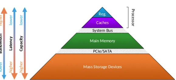
Memory is characterized by three properties:latency,capacityandbandwidth.
Latency is the time between requesting data at a particular memory address and when the data is delivered by the memory. Capacity is the amount of data that can be stored in a memory and bandwidth (or throughput) is the amount of data that can be transfered in a certain time frame, usually measured inBits per second(Bit/s). Figure 2.2shows a schematic illustration of the memory hierarchy of a computer. We already mentioned that processors have registers to store intermediate results. These registers are extremely fast, have a very low latency but are very limited in size. To work on large amounts of data, computers have a main memory that is slower but much bigger. It can be accessed through the system bus of the processor. As data is often used multiple times,cachesare used
on the data path between main memory and registers to temporarily store data. This allows to quickly access data that has been read before, without keeping it in a register. As caches do not only load single data words but entire data lines, they also improve access to neighboring data. Caches can only store a small fraction of the data, as they are significantly smaller than the system memory. Therefore, special strategies are used to ensure that only data resides in the caches, which is most likely be used [Patterson and Hennessy 2013, p. 457]. If the size of the main
PCIe/SATA System Bus Reg. La ten cy lo w er hi gh er Ba nd w id th h ig h er lo w er Ca p ac it y lo w er hi gh er
Mass Storage Devices Main Memory Caches P ro ce ss o r
Figure 2.2: Memory hierarchy of a computer. With increasing bandwidth, the latency improves but the capacity decreases [Patterson and Hennessy 2013, p. 454]. memory does not suffice, or data is supposed to be stored permanently, to make it available after powering down the machine, massive storage devices are used. Their capacity is significantly larger than of the main memory, but they are also significantly slower. To improve the performance, caches can be used between the main memory and the storage device. Overall we see that in the worst case, data has to go through all levels of the memory hierarchy to get to the processor, which can quite some time as the latency of all levels is summed up.
2.1.3
Multi-Tasking and Scheduling
On a computer usually multiple applications are running simultaneously (e.g., a browser, text processing or image viewing applications) and each of these appli-cations itself is executed as a separateprocess. As all of these have to share the
same compute resources, it is necessary to apply a schedule that defines which application is allowed to use the processor at a certain time. Basic scheduling algorithms (e.g., round robin), define a strict schedule when and for how long an application is allowed to use the compute resources. While this scheduling method is easy to implement it does not guarantee to yield good performance. Applications can be put to hold, as long as they wait for data, allowing others that have their data available can continue their computations. This concept is calledlatency hidingand is actively used at multiple levels in the processor, not
only on an application level. Within the same application it is possible to have multiple active separated calculations, calledthreads. In general it produces a
certain overhead to switch between different applications as the data in registers has to be stored in another location, wherefore another application or thread can use them for its calculations.
+0 +1 +2 +3 +0 +1 +2 +3 +0 +1 +2 +3 +0 +1 +2 +3
Execution Time
+ + + + 1 0 1 2 3 4 5 6 7 8 9 10 11 12 13 14 15 0 2 3 4 5 6 7 8 9 10 11 12 13 14 15 1 0 1 2 3 4 5 6 7 8 9 10 11 12 13 14 15 0 2 3 4 5 6 7 8 9 10 11 12 13 14 15In
st
ru
ct
io
ns
se
ri
a
l
p
ip
el
in
ed
Figure 2.3: Simple pipeline example. The pipelined variant requires only seven cycles, compared to 16 in the purely serial variant.
2.1.4
Processing Improvements
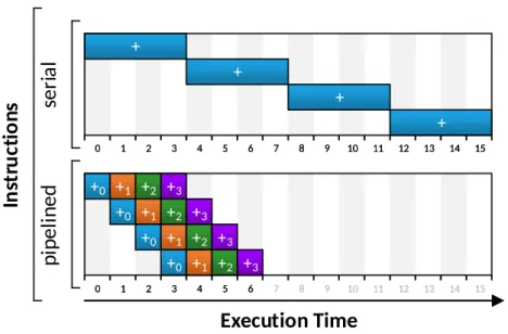
Executing one operation after each other is very costly, as the next calculation has to wait until the first is complete. Therefore,Instruction Level Parallelism
(ILP)[Patterson and Hennessy 2013, p. 391] is used to better utilize the compute resources. There are two kinds of ILP. First, it is possible to divide calculation operations into a series of stages. Normally, operations (e.g., an addition) require several clock cycles. To better utilize the operation unit it is fed with new data in every clock cycle. In every following cycle the data is passed to the next stage of the operation. This technique is calledpipeliningand is illustrated inFigure 2.3.
The second method is to provide multiple PUs that can be used in parallel. However, this method requires that the code allows to map different instructions onto the PUs. This mapping can be done in a static way [Patterson and Hennessy 2013, p. 393] during programming of the application.Very Long Instruction Word(VLIW) processors require this kind of programs. Other processors (calledsuperscalar)
do this mapping on-the-fly by analyzing the code before execution [Patterson and Hennessy 2013, p. 397].Figure 2.4shows an example code that can be executed on two different PUs in parallel. Of course, both ILP methods can also be combined.
2.1.5
Multi-Processing
Another method to improve the performance of a computer ismulti-processing.
int a = 1; a = a + 5; int b = 2; b = b + 7; int c = a + b; c = c + 3; int a = 1; int b = 2; a = a + 5; b = b + 7; int c = a + b; c = c + 3;
Serial
DDG
Instruction Parallelized
PU0 PU1
Figure 2.4:Simple superscalar ILP example. The serial code (left), its corresponding data dependency graph (center) and how this code is executed in a reordered ILP manner (right). As can be seen, the first operations onaandbare independent of each other and can be processed in parallel. Starting with initialization of variable c, the execution depends on the results ofaandb.
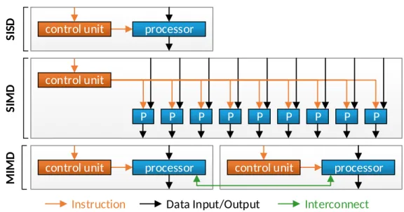
There are four different processing types categorized by Flynn’s Taxonomy [Flynn 1966]. The first category describes serial processors asSingle Instruction, Single Data(SISD)processors. This also includes processors that utilize ILP. In some appli-cations it is possible to process data in a vector fashion. Here, the same operation is applied to a set of data and therefore it is specified asSingle Instruction, Multi-ple Data(SIMD). The third option is to use multiple processors that can operate separately on the data, calledMultiple Instruction, Multiple Data(MIMD). Flynn’s Taxonomy also specifies theMultiple Instruction, Single Data(MISD), but there is no known implementation today, as it can just be implemented using a MIMD architecture. Figure 2.5shows an example of the different architectures. The previously described multi-tasking can be easily realized with the MIMD pattern, as a process or task can be mapped onto a single processor. In contrast, it is not possible to map this onto SIMD processors as there only one instruction can be handled at the same time.
One of the biggest problem of parallel processing (besides developing suitable algorithms that leverage enough parallelism to be efficient) arerace conditions, dead locksandhazards. Race conditions are timing problems, so that the outcome
of an algorithm might be random. For example, if an algorithm is supposed to count the occurrences of a specific value in a list, a processor has to read the current count, increase the value and write it back. If another processor updates the value, between the read and write of the first processor, the result will be wrong. Dead locks appear whenever parallel threads reserve resources exclusively that are also required by other threads. For example, if two threads require two
control unit processor
control unit
P P P P P P P P
control unit processor control unit processor
Instruction Data Input/Output Interconnect
P SI MD SI SD MI MD
Figure 2.5:Example for a SISD, SIMD and MIMD architecture. MIMD architectures not necessarily have to consist of SISD units, but could also consist of SIMD units. resources (AandB) and the first grabsAwhile the second takesB, both wait for
the other resource to be released, which will never happen. Hazards occur when data is accessed in parallel. These may or may not be problematic. For example, when multiple threads write data to the same memory cell, it is undetermined, which data will be stored in the end. However, if all threads write the same value, it does not matter as the result is always the same. To prevent hazards efficiently, atomic operations can be used to enforce certain constraints, e.g., to store the max value. Cases where data is read from a cell that was previously overwritten by another thread can be problematic. Without explicit synchronization it is not guaranteed that all threads read the new value, depending on the execution order on the device.
2.1.6
Performance Classification
So far we have introduced how computers work and some techniques that are used to improve the performance through parallelism. To be able to compare the performance of different processors, it is necessary to find a suitable metric. For a simple processor without any ILP and multi-processing capabilities, where each instruction requires exactly one clock cycle, it is possible to compare these processors by their clock frequency. However, with all of our improvements, this measure is not sufficient. Therefore, today measures such as Cycles Per Instruction(CPI),Instructions per Second(IPS)orFloating Point Opterations Per Second(FLOPS)[Patterson and Hennessy 2013, p. 70] are used, depending on the
Processor0 Processor1 Processor2 Processor3
Figure 2.6:Parallel search for maximum value of a list with 16 numbers, on four processors.
application of the processor. To calculate the improvement (also calledspeedup(S))
of a specific application on different processors or to determine the improvement achieved through parallelization of code, the ratio betweenoriginal execution time
(Toriginal) andoptimizedorparallelized execution time(Toptimized) can be calculated.
S = TToriginal
optimized (2.1)
Unfortunately, applications can never be entirely parallelized, so that their execu-tion time consists always of aserial(Tserial) and aparallel(Tparallel) fraction, withp
as the number of parallel processors.
Ttotal =Tserial+Tparallelp (2.2)
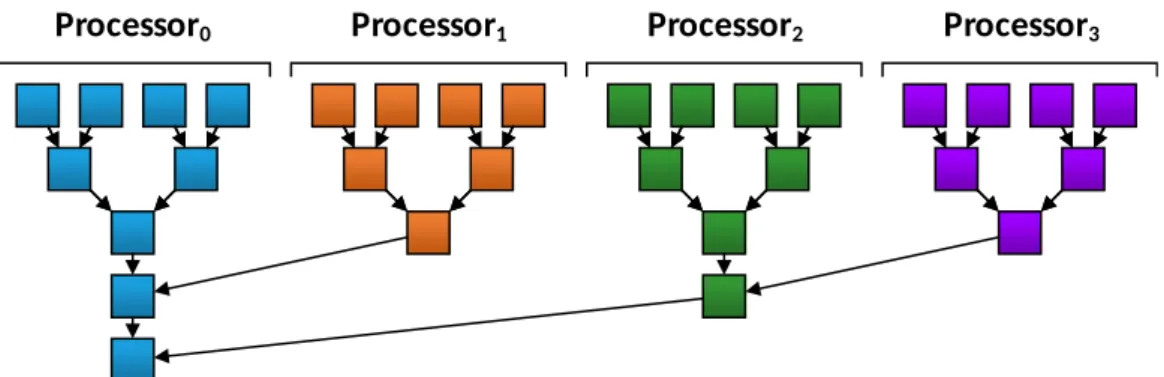
Additionally, it is common that parallel algorithms require more operations com-pared to serial algorithms. This is necessary as parallel algorithms often have to aggregate the results across the parallel processors. For example, to find the maximum value of a list on a serial processor, all elements have to be processed, which results in a linear complexity ofO(n).Figure 2.6shows a multi-processor
and how a parallel algorithm would process the elements. As can be seen, it requires significantly less processing steps (5 vs. 16), but it is only 3.2x faster and not 4x as a perfect speed up would suggest.
2.1.7
Performance Limitations
Overall we can see that the performance of an application can be limited by three factors:
1. By latency, if the application has to wait too long for data to arrive at the processor.
2. By bandwidth, if the memory is unable to provide enough data in time. 3. By computation, if there are not enough computational resources or the
computation itself depends on too many intermediate results.
2.2
Hardware Implementations
In this section, we dive deeper into the actual implementation of processors, memory and storage devices. The processor of a computer is called CPU, which also describes the type of processor. CPUs cores are optimized for serial processing performance. To utilize parallelism, processors can be placed in separate chips and interconnected by a bus, which are called multi-CPU systems, or multiple processors can be placed into the same chip, which are called multi-core CPUs. Every sub-processor in such a CPU is called acore. The on-chip memory hierarchy
(registers and caches) of CPUs usually have multiple layers of different caches. The system memory (calledRandom Access Memory(RAM)) traditionally is placed in a separate hardware component. Depending on the application RAM can also be directly embedded into the same chip together with the processor. This not only reduces the energy consumption but also the signal latency. As today’s RAM is usually manufactured asDynamic RAM(DRAM), temporary data is lost as soon as the power to the device is turned off. Therefore, mass storage devices are used to permanently store data. Traditionally this task was performed byHard Drive Disks(HDDs), but in recent years these are more and more replaced bySolid State Disks(SSDs). The difference is that HDDs store their data on magnetic disks while SSDs store the data in non-mechanical memory chips. This property makes SSDs more durable in terms of physical damage, while also reducing the weight, size and significantly improves the access performance. However, there are concerns that the SSD’s live cycle is lower than of HDDs because their memory cells deteriorate with every write operation. Experiments as conducted byGasior [2014]proofed that even consumer SSDs can survive over 2PB of written data. The reason for the high performance of SSDs compared to HDDs is that instead of physical readers for the magnetic disks (that need to be repositioned to access a memory cell) SSDs can directly access their memory cells. Despite the advantages of SSDs, HDDs are still used because of their high storage capacity and lower prices. There are also other techniques to permanently store data directly inside the RAM, called
Component Model Capacity Latency Bandwidth Reference
CPU Intel I7-6770 few kB 4-49 ns [7-CPU 2016] RAM DDR4-2400 CL17 1-16 GB 14.17 ns 18.75 GB/s [CRUCIAL 2015] SSD Samsung 960 Pro M.2 512GB - 2TB 21.9 µs 2.25 GB/s [Armstrong 2016] HDD WD4001FAEX 4TB 6.62 ms 148.55 MB/s [Tom's Hardware 2017] Table 2.1: Exemplary properties of a CPU, RAM, SSD and HDD. As can be seen, with increasing capacity the latency significantly increases while the bandwidth decreases.
Non-volatile RAM (NVRAM). NVRAM is a categorical term describing various technologies, e.g.,Static RAM(SRAM)combined with a battery, Ferrorelectric RAM(FeRAM),Magnetoresitive RAM(MRAM)orPhase-change RAM(PCRAM). These technologies are still very expensive and hardly used in today’s computer systems. The latency, capacity and bandwidth of these components greatly differs, as shown inTable 2.1.
2.2.1
Bus Systems
In order to connect all components of a computer (e.g., HDD, RAM and CPU) an interconnection bus is required. The main bus of a computer is thesystem bus. It
usually connects the CPU with the RAM. Further, it comes with an I/O component that can attach other buses. Depending on the topology of the computer, e.g., if it is equipped with multiple processors, the system bus also connects the dif-ferent CPUs (e.g., using Intel’sQuickPath Interconnect(QPI)[INTEL 2009]). Other components are usually connected using thePeripheral Component Interconnect Express(PCIe)[PCI-SIG 2010] bus. It was introduced in 2004 and is currently re-leased in the third revision. PCIe uses lanes, which also can be clustered to transfer more data in parallel. Up to 32 lanes are possible, whereas maximal 16 lanes are used today, leading up to 15.75GB/s1total bandwidth. PCIe can be used to connect
all kinds of components. A more specialized bus is theSerial AT Attachment(SATA) bus that is used for HDDs and SSDs. For SSDs also PCIe can be used, due to the higher bandwidth.Figure 2.7shows an illustration of a multi-processor topology.
2.2.2
Processor Performance
Traditionally the speed of a hardware components is defined by its clock frequency. To increase the performance it is possible to raise the clock frequency. In the
18GT/s· 2 |{z} full duplex ·128Bit/130T | {z } encoding =15.75GB/s
RAM0 CPU0 CPU1 RAM1 RAM2 RAM3 Network GPU0 SSD HDD SSD SATA Controller GPU1 QPI SATA P C Ie PCIe
Figure 2.7:Illustration of the bus topology of a two-processor system with four RAM modules and some additional components such as storage drives, controller and accelerators.
past this was usually limited by the size of the manufacturing technique of the processors. If the feature size of the chip is too big and the frequency too high, there is not enough time for the electrons to travel through the circuits before the next cycle starts. Electrons in silicon travel at max 107cm/s (known asvelocity saturation) [Yu and Cardona 2010, p. 226], so with a frequency of 3GHz these can
only travel up to 33.33µm until the next clock cycle. This leads also to the fact that the smaller a transistor is, the faster it can operate. Therefore, the clock frequency was increased every time manufacturers have been able to produce chips with a decreasing feature size.Moore [1965]predicted that the number of transistors would duplicate approximately every two years. This increase would improve the processor performance at the same rate. Since its proclamation in 1965, Moore’s law was more or less accurate. With more and faster transistors, manufacturers have been able to constantly improve the performance of processors.
However, in the last decade the advances in shrinking the feature size have been slowed down, as the manufacturing processes reached physical limitations [ Berke-ley 2014]. There are multiple reasons for this limitation. First, it became more and more difficult to create methods that are able to produce small enough structures in the silicon. The second reason is heat. Every time a transistor is switched it consumes energy, which produces heat. With increasing clock frequency the tran-sistors are switched more often, creating more heat in less time. To compensate for this increased heat, the voltage that is driving the transistors has to be reduced. However, as components require a certain minimum voltage, it cannot be reduced infinitively. Another phenomenon is electric leakage. This is an electric current that is lost even when an electric component is not actually switched. The leakage increases with smaller feature sizes. Methods as presented byZhang et al. [2005]
shrink the feature size and to reduce effects such as the electric leakage has slowed down in recent years. More information on the topic can be found inAhmed and Schuegraf [2011]. We can summarize that the methods that were able to drive the development do no longer work and other solutions have to be found.
2.2.3
Caches for Parallel Processing
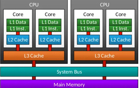
Before we introduce different parallel processor implementations, we take a closer look on caches in parallel processors. As previously mentioned, caches are used to store data directly in the processor for faster access. With parallel processors systems, multiple processing units access the same RAM and therefore utilize the same caches. To achieve high performance, cache hierarchies are used. There are multiple levels of caches, where some of the caches only serve a single core, while others serve a group or all cores. Every level has to be kept synchronized with the next higher level to ensure that processors work on the correct data. The higher a cache is in the hierarchy, the bigger its size and latency. Depending on the processor the number of caches can differ. Today two or three layers are normally used.Figure 2.8shows an example cache hierarchy used in today’s processors. If the left processor changes a value and stores the result in its L1 cache, the result has to be communicated to the other cores, otherwise they will use outdated data. There are many ways for ensure synchronization, depending on the processor’s purpose, implementation and features used [Patterson and Hennessy 2013, pp. 534].
2.2.4
Parallel Processors and Accelerators
The meaning of the term MIMD is very wide, as it describes not only multi-processor, multi-core but also any interconnected compute cluster. It therefore is difficult to pinpoint an exact date when the first MIMD devices appeared. One of the first articles about multi-processing has been published byKrajewski [1985][p. 171-181]. In 2005 the first consumer multi-core processors where introduced [INTEL 2005], where multiple processor cores have been put onto the same chip. One problem of processors is the thread switching, which can be costly.Simultaneous Multithreading(SMT)is a solution for this thread switching. It provides multiple register sets that can be switched efficiently without copying the data to another memory. One implementation is Intel’sHyperThreading[INTEL 2002] technology.
The first implementations of SIMD instructions for consumer CPUs have been In-tel’s Multi Media Extension(MMX)[INTEL 1997] andAMD’s 3DNow![AMD 2000].
Todays CPUs support AVX with up to 512Bit wide operations [Reinders 2013]. To use these SIMD capabilities, the code has to explicitly use the corresponding SIMD
CPU CPU
Core Core Core Core
Main Memory L1 Data L1 Inst. L1 Data L1 Inst. L1 Data L1 Inst. L1 Data L1 Inst. L3 Cache L3 Cache System Bus
L2 Cache L2 Cache L2 Cache L2 Cache
Figure 2.8:Schematic view of a 3-layer cache hierarchy in a multi-core setup with two CPUs. As can be seen, the L1 and L2 caches are placed in the cores, so that when one core changes a value, the change has to be propagated to the other cores to ensure consistency. Same applies for the two CPUs.
instructions. Unfortunately, not all CPUs support all techniques and commands, so it is necessary to check, which instructions are supported. Luckily, projects as theIntel Single-Program Multiple-Data Program Compiler(ISPC)[Babokin and
Brodman 2016] try to automatically parallelize code for SIMD CPUs. However, with multi-core and SIMD instructions, CPUs are still mostly tuned for serial perfor-mance and support only few parallel workloads. In the mid-90’s GPUs [Glatter 2015] have been introduced. However, their design has been very crude compared to todays GPUs. Initially they have been solely designed for 3D rendering. Never-theless, their design evolved and today they are massively parallel processors with up to several thousand cores in a single chip. In some early developments [Buck et al. 2004] the rendering pipeline of GPUs have been misused to accelerate cer-tain procedures, e.g., matrix multiplications. Later easier programming languages have emerged such as CUDA that we will introduce inSection 3.1.
Other approaches are the Intel Xeon Phi [INTEL 2013b], which puts up to 72 cores onto a chip and is a mixture of a massively parallel GPU and a multi-core CPU, also calledMany Integrated Core(MIC)architecture. In general manufacturers have to find a trade off between serial processing, leading to fewer but faster cores, and parallel processing, resulting in slower but much higher numbers of cores.
Further, there are many different ways to interconnect processors. Multi-CPU systems are usually interconnected by buses such as Intel’s QPI. Accelerators operate usually as slave devices in workstation or server computers, connected using PCIe. Atop of these computers, it is possible to interconnected these to clusters by different types of network adapters, based oncopperorfibercables.
Interconnects such as InfiniBand are trimmed for bandwidth and low latency [InfiniBand 2016] and are usually used in computer clusters. These again can be built tightly interconnected cluster or as a loosely coupled compute cloud [Buyya et al. 2009].
However parallel processing and higher clock frequencies are not the only way to speed up computations. For certain application-domains, specialized processors such asDigital Signal Processings(DSPs), the Epiphany-V (a 1024-core processor) [Olofsson 2016] or Google’s TPU [Jouppi 2016] exist that are specially designed to operate efficiently on the operations needed for these applications. They usually provide specialized hardware processing units. Sometimes, if the application is not altered, e.g., in video de-/encoding, the algorithm itself is put into hardware (so-calledApplication Specific Integrated Circuits(ASIC)), without any means of altering after it has been manufactured. This results in the best possible performance per energy consumption ratio, but bears the danger of implementation error on the chip, which require to be explicitly replace the entire component. More general areField Programmable Gate Array(FPGA)which can be reconfigured but also translate the program they are executed directly into hardware. Although they usually have a very low clock frequency compared to CPUs, they can achieve much higher performance in specialized applications or when non-standard variable types are used. Many studies have been performed on different application fields, concluding varying results rather a FPGA, CPU or GPU is better [Chase et al. 2008;
Papadonikolakis et al. 2009;Pauwels et al. 2011]. Except for CPUs, processors are usually designed to function as slaves. This prevents them from operating on their own, so they must be controlled by a master CPU.
2.2.5
Graphic Processing Units
As the main focus of this thesis is on GPUs, we take a deeper look into their imple-mentation. GPUs have been specifically designed to run thousands of calculations in parallel. Therefore, their cores are much simpler than those of CPUs, with less features and a lower clock frequency but their high number of processing cores compensates for this. The advantage of GPUs is, because of their SIMD architec-ture, that groups of cores perform the same operation in parallel so that not each single core requires its own controlling infrastructure. Instead the cores can be grouped together in so-calledSIMD groups, as all of them are supposed to execute
the same operation. GPUs can be integrated into a computer in different ways. Traditionally they are extension cards that are either attached using PCIe or with the recently introduced NVLink [NVIDIA 2014c] bus that provides higher bandwidth than PCIe which requires special support from the CPU. So far only IBM’s Power processors [Gupta 2016] are announced to support NVLink. Another option is to put the GPU directly onto the mainboard (usually referred as“on-board GPU”). In
these cases the GPU is still attached to the CPU using PCIe.
Due to the low bandwidth of PCIe compared to the bandwidth of the system memory, PCIe attached GPUs are equipped with their own memory. This requires to explicitly copy data between the system memory and the GPU. This copy can become a major bottleneck in many applications. Manufacturers such as Intel or AMD therefore provide CPUs with directly integrated GPUs. This allows the GPUs to be directly attached to the system bus and access the main memory. This is, e.g., done in AMD’sAccelerated Processing Unit(APU)[Gaster and Howes
2011]. However, in these combinations CPU and GPU shared the same chip and are usually only providing limited compute performance, as both produce heat on the chip. AMD wants to remove these limitations in their recently proposed
Exascale Heterogeneous Processor(EHP)[Vijayaragavan et al. 2017] that aims at an even tighter coupling of cache coherent CPU and GPU cores, using fast on-chip and slow but bigger off-chip memory, which can be accessed by all CPU and GPU cores of the processor.
Today there are different types of GPUs available. Intel focuses mainly on low-end and multimedia GPUs that require only a small amount of energy and therefore can be especially used in low-power and mobile systems. The same applies for the Mali GPUs from ARM, which are specifically trimmed for smart phone applications. These GPUs provide only limited compute capabilities. Matrox mainly provides GPUs for multi-display setups in professional environments with advanced features, low-energy consumption and high reliability. AMD is mainly established in low-end and gaming GPUs. The latter type aims at providing high performance for real-time 3D rendering applications. To expand onto theHigh Performance Computing(HPC) market, they recently released theRadeon InstinctGPUs [Hook and Graves 2016].
NVIDIA tries to provide GPUs for the entire market from low-end (GT-series), over gaming (GTX-series), professional (Quadro-series) up to HPC (Tesla-series). The GT-series is meant for multimedia applications and comes with very limited compute capabilities requiring only a low amount of energy. The GTX series is usually optimized for high single precision float performance. The Quadro-series aims at providing professional features, comparable to the GPUs from Matrox, an advanced multi-display support, or features such as GPUdirect, which enables to directly access the memory of a GPU from other devices that are connected to the PCIe bus. The Tesla-series aims at high performance, providing excellent
performance for single and double precision float computation. However, Tesla GPUs usually do not have any display ports and therefore can only be used as compute accelerator which cannot be attached to a monitor.
2.2.6
Memory Types
As we have already mentioned, there are many different kinds of memory types build into a computer, ranging from registers, caches, RAM up to storage devices. Over time there have been significant changes to how RAM has been implemented. TraditionallySynchronous Dynamic RAM(SD-RAM)was used in computers, trans-ferring one data word at the positive clock edge, over a 64Bit interface. This was later improved byDouble Data Rate(DDR)SD-RAM which not only transferred data by the positive but also the negative clock edge. The memory loads two data words into a message buffer and then transfers the data. This method is called 2n-prefetch. Today the fourth revision of DDR is used, which still uses a 64Bit interface but a 8n-prefetch, resulting in much higher external clock frequencies.
Figure 2.9shows an illustration of the differences between SD-RAM and DDR. As GPUs are massively parallel processors, with hundreds or thousands of active cores, specializedGraphics DDR(GDDR)has been developed, which is a modified version of DDR memory with extended bus width. TodayGDDR5with 8n-prefetch
orGDDR5Xwith 16n-prefetch are used. Further,High Bandwidth Memory(HBM) [AMD 2015] has been proposed as successor for GDDR. For HBM, multiple DRAM modules are stacked atop of each other. To transfer the data to the processor, a wide memory interface is used – significantly wider as for DDR or GDDR modules. As currently HBM is still expensive to manufacture, it is mainly used in high end gaming (e.g., AMD Radeon R9 Fury Series [Macri 2015]) or HPC GPUs (e.g., NVIDIA Tesla P100 [NVIDIA 2016d]).
2.3
Array Layouts
Arrays are one of the most important building blocks in applications. As hardware architectures use certain cache hierarchies, strategies, memory technologies and buses, it is important to optimize the access to the data in an array. Arrays can be one- or multi-dimensional and consist of scalar or multiple data fields or even contain sub-arrays. Therefore, the structure of an array can have a significant impact on the performance if used in an inadequate way.
2.3.1
Multidimensional Indexing
Every multi-dimensional array has to be stored in a linearized manner. The way this is done can be arbitrary as long as every entry is mapped to one unique index.
SD
DDR I/O
Buffer
CPU
CPU
RAM System Bus Proc.
Figure 2.9: Illustration of how SD-RAM and DDR works. DDR is shown for 2n-prefetch, other modes work the same way. The SD-RAM only transfers one data package per clock cycle. In contrast DDR loads two data packages into an I/O buffer and transfers one of these at each clock edge.
M00 M01 M02 M03 M10 M11 M12 M13 M20 M21 M22 M23 M30 M31 M32 M33 M00 M01 M02 M03 M10 M11 M12 M13 M20 M21 M22 M23 M30 M31 M32 M33 M00 M01 M02 M03 M10 M11 M12 M13 M20 M21 M22 M23 M30 M31 M32 M33 M00 M01 M02 M03 M10 M11 M12 M20 M21 M30
Figure 2.10: From left to right:two different linear transpositions, z-order curve and triangular matrix.
Usually this is done by a simple linearization such asx +y∗ |x|as it is easy and
fast to compute. However, in some applications more complex schemes such as the z-order curve [Morton 1966] yields in better results.Figure 2.10shows some examples for different indexing schemes. For simple linearizations of the form
x +y∗ |x|the number of possible combinations is defined by the factorial of the
number of dimensions, so that a 5D array has 120 different linearizations.
2.3.2
Struct Layouts
Another type of arrays contains no primitive types, but structures. These are calledArray of Structs(AoS). In an AoS data that belongs to the same index is stored in one block. For parallel applications this works well, when each thread accesses the entire struct data at the same moment. It performs badly, when only one of the components is used at the same time. In this case, aStructure of Arrays(SoA)performs better. Here, every component is stored in a separate array. This is also the format that the NVIDIA Programming Guide [NVIDIA 2016a] recommends. However, one disadvantage of the SoA is that its implementation
0 0 0 1 1 1 2 2 2 3 3 3 0 1 2 3 0 1 2 3 4 5 6 7 0 1 0 1 0 1 2 3 2 3 2 3 0 0 1 1 2 2 3 3 0 1 2 AoS SoA AoSoA SoAoS1 4 4 4 5 5 5 6 6 6 7 7 7 4 5 6 7 4 5 6 7 0 1 2 3 4 5 4 5 4 5 6 7 6 7 6 7 4 4 5 5 6 6 7 7 SoAoS2 SoAoS3 4 5 6 7 3 0 0 1 1 2 2 3 3 4 4 5 5 6 6 7 7 0 1 2 3 4 5 6 7 0 0 1 1 2 2 3 3 4 4 5 5 6 6 7 7 0 1 2 3 4 5 6 7
Figure 2.11: Different ways to store the data of a struct array with three child items (orange, green and blue). The AoS stores all of the components of the same index next to each other. In contrast, the SoA groups all elements of the same component together. AoSoA is a hybrid, that stores groups in a SoA way. SoAoS stores parts of the array as AoS and other as SoA.
either requires more registers, as the root pointers to each sub-array have to be stored, or the root pointers have to be explicitly recalculated every time the array is accessed. In general it can be said that SoA requires more registers than an equivalent AoS. If memory access is a bottle neck, this additional resource or compute overhead can be less than the benefit gained from the improved memory utilization. Further, there are also hybrid formats such asArray of Structure of Arrays(AoSoA)(sometimes also referenced astiled-AoS[Kofler et al. 2015] or Array-of-Structure-of-Tiled-Arrays(ASTA)[Sung et al. 2012]) which are a hybrid of AoS and SoA. In AoSoA, small tiles of data are stored in a SoA-style, while these tiles themselves are organized in an AoS-way. The size of the tiles is application depending, but for GPUs using a size equal to the SIMD-group size proved to work well in many scenarios. One disadvantage of AoSoA is that in the last part of the array, memory is wasted, if the number of elements cannot be divided by the tile-size. Changing the layout of a AoS is not the only transformation that can be applied. The AoS itself can also be divided into different arrays, where each of the resulting arrays can be stored in a different layout. Peng et al. [2016]refer this asStructure of Array of Structures(SoAoS). They use a AoS and store one part as SoA and the other as AoS. InFigure 2.11we show how the data is stored for the mentioned layouts. Further,Listing 2.1shows the differences in register and computational requirements for AoS, SoA and AoSoA.
1 /****************************** AoS ******************************/
2 // Registers: 3 (array, index, address)
3 // Operations: 3 (2x add., 1x mult.)
4 struct AoS { | address = index + 2;
5 int A, B, C D; | address = address * sizeof(int);
6 } array*; | address = address + array;
7 array[index].C; |
8
9 /************************* SoA, variant A ************************/
10 // Registers: 6 (array.{A,B,C,D}, index, address)
11 // Operations: 2 (1x add., 1x mult.)
12 struct SoA { | address = index * sizeof(int);
13 int *A, *B, *C, *D; | address = address + array.C;
14 } array; |
15 array.C[index]; |
16
17 /************************* SoA, variant B ************************/
18 // Registers: 4 (array, index, count, address)
19 // Operations: 4 (2x add., 2x mult.)
20 int* array; | address = count * 2;
21 array[index + 2 * count]; | address = address + index;
22 | address = address * sizeof(int);
23 | address = address + array;
24
25 /************************ AoSoA (2-tiles) ************************/
26 // Registers: 4 (array, index, address, temp)
27 // Operations: 6 (3x add., 1x mult., 1x div., 1x mod.)
28 struct AoSoA { | address = index % 2;
29 int A[2], B[2], C[2], D[2]; | address = address + 4;
30 } array*; | temp = index / 2;
31 array[index / 2].C[index % 2]; | address = address + temp;
32 | address = address * sizeof(int);
33 | address = address + array;
Listing 2.1:Example for AoS, SoA (in two different implementations) and AoSoA. Left: Description of the data layout and an exemplary access to the item
array[index].C. Right: Necessary calculations to acquire the address of the
item.Registersandoperationsindicate how many registers and calculations are
Target Architecture and Platform
This chapter gives an overview of NVIDIA’s CUDA (Section 3.1) and all NVIDIA GPU architectures (Section 3.2) that can still be used with the current CUDA toolkit. This covers four hardware generations, ranging from the“Fermi”up to the most
recent“Pascal”architecture.
3.1
NVIDIA CUDA
CUDA [NVIDIA 2016a] was introduced by NVIDIA in 2007. It is the standard for non-graphical compute intensive programming for NVIDIA GPUs. CUDA stands for“Compute Unified Device Architecture”and is specifically designed to model
massively parallel computations. CUDA consists of a compute model and a pro-gramming language, which will be explained in detail in the following sections. There are also competing programming languages such as OpenCL1, OpenACC2
and C++ AMP3. We do not explain these in this thesis, as our research concentrates
on CUDA.
3.1.1
Compute Model
The CUDA compute model is designed for massively parallel processors. As GPUs implement the SIMD scheme, these organize threads in SIMD groups, which are calledwarps. Since the beginning of CUDA, a warp consisted of 32 threads, whereas
in the early versions only 16 of them had been active at the same time. This limitation is no longer present in newer GPUs. Multiple warps are grouped in so calledblocks. The current maximum is 1024 threads or 32 warps respectively,
per block. During the execution, one block is mapped onto oneStreaming Multi-Processor(SM)on the GPU. This concept is illustrated inFigure 3.1. These multi-processors usually consist of hundreds of small cores, where one thread is mapped to one of the cores. The GPU threads are very light weight, so that whenever one warp stalls – because it has to wait for memory to be accessed – it can be immediately replaced by another idle warp of the same block with very little swapping overhead. This method is comparable to Intel’s HyperThreading [INTEL
1www.khronos.org/opencl 2www.openacc.org