International Journal of New Technology and Research (IJNTR) ISSN:2454-4116, Volume-3, Issue-9, September 2017 Pages 108-113
108 www.ijntr.org
An Experimentation Framework for Project- Based
Learning in Electronics
O. A. Ogungbenro, G. A. Chukwudebe, F. K. Opara , G. N. Ezeh
Abstract- In this paper, an Experimentation Framework for project-based learning in Electronics is developed to bridge the gap in practical electronics mastery amongst undergraduates
of electrical engineering. The framework comprises of an
Electronics Laboratory Trainer (AEL-350) and a practical handbook. The All-in-One Electronics Laboratory Trainer (AEL-350) can be used for the conventional hardware experiments, in addition to component emulation where the components are not easily available. Additionally, the practical handbook which doubles as a manual and a tutorial is written for the Laboratory Trainer. Microcontrollers and multiple
displays formed the heart of the design of the Electronics
Laboratory Trainer. Proteus, Livewire and Eagle PCB Simulation software were used for circuit design and simulation. Also MIDE compiler was used to debug the embedded C Program. The AEL-350 Trainer has several on-board components and sensors, multiple-outputs double rail power supply unit, 8-bit TTL outputs and inputs, de-bounced clock, peripheral interface controller and double-sized breadboard to make it flexible for users to perform up to 350 experiments and projects for mastery of electronics design and implementation. The AEL-350 is portable, with a dimension of 36cm x 35cm.
Index Term-: Experimentation Framework. Project-based learning. Circuit Emulation. Microcontrollers. Electronics Trainer.
I. INTRODUCTION
Although, Nigeria and many other sub-Saharan African countries have been producing graduates in electro-technology from higher institutions and technical colleges for over forty years, all electronic gadgets and equipment are still imported from the western world. The graduates do not seem to acquire the requisite practical knowledge of electronics while in the school. Employers find most graduates unable to support or reconfigure electronic equipment when challenged.
A study carried out revealed that part of the problem is the method of teaching electronics in schools. For the practical, one of the mostly used equipment is the Electronics Laboratory Trainer.
O. A. Ogungbenro, Department of Electrical/Electronics, Federal
University of Technology, Owerri, Nigeria.
G. A. Chukwudebe, Department of Electrical/Electronics, Federal
University of Technology, Owerri, Nigeria.
F. K. Opara , Department of Electrical/Electronics, Federal University of
Technology, Owerri, Nigeria.
G. N. Ezeh, Department of Electrical/Electronics, Federal University of
Technology, Owerri, Nigeria.
Different types of Electronics Laboratory Trainer systems are already developed for various applications. The common goal of all is to make electronics laboratory practical easier, enjoyable and understandable to students. However, the Electronics Laboratory Trainer systems are expensive; many schools do not acquire enough units. Consequently, the students do not have adequate access time for hands-on training. Additionally, most of the experiments designed for use on the lab trainers are to verify
laws and theorems. Thus, the prevailing teaching method, whereby lectures are delivered in the classrooms and lab trainers are used to verify laws do not ensure that graduates can design and build systems.
This traditional method limits students to primitive and stereotype reasoning instead of creative and adaptive reasoning. The teaching and learning method for electronics have since changed to integrated and project-based learning. Project-Based Learning (PBL) is a model that organizes learning around projects. Project-based learning was promoted bythe Buck Institute for Educationin the late 1990s, in response to school reform efforts of that time (Thomas, 1998; Jones, Rasmussen, & Moffitt, 1997; Thomas, Mergendoller, & Michaelson, 1999). Project-based learning provides students with complex tasks based on challenging questions or problems that involve the students' problem solving, decision making, investigative skills, and reflection that includes teacher facilitation, but not direction. Project-based learning approach has the potential to fill the gap in teaching and learning electronics. It offers a wide range of benefits to both students and teachers. For students, the benefits of project-based learning include: increased attendance, growth in self-reliance, opportunities to develop complex skills, such as higher-order thinking, problem-solving, collaboration, communication and improved attitudes toward learning (Thomas, 2000), (Boaler, 1997; SRI, 2000 ), (SRI, 2000).
In this paper, an experimentation platform for project-based learning in electronics is developed and used to implement an affordable electronics trainer which can be used to perform up to 350 experiments and projects for improved acquisition of sound practical electronics knowledge.
II. MATERIALS AND METHODS
A. The Experimentation Framework for Project-Based Learning in Electronics
After careful review of the literature on project-based learning and electronics teaching aids currently in use, it became obvious that the requirement for the development of an experimentation framework for project-based learning in electronics will incorporate multiple factors. These will include the design and construction of the electronics laboratory trainer and the development of a user enhanced practical manual/handbook with instructions on how to use the trainer and how to design electronic circuits. The amalgamation of these two requirements will provide the platform for the design methodology for the development of experimentation framework for project-based learning in electronics. This paper concentrates on the first requirement, design of the electronics laboratory trainer. The Electronics Laboratory Trainer is designed to provide for a user to be able to perform many experiments and build up to 350 electronic circuits and projects; hence it has been named “All in One Electronics Laboratory” (AEL-350). The Trainer can be used for running laboratory experiments in colleges, polytechnics and universities, as well as by hobbyist or students who want to learn electronics on their own.
B. Materials Used for the Design and Implementation of the “All-in-One Electronics Laboratory” (AEL-350) Trainer
With direct reference to the design requirements, the materials and methods used for both the hardware and software aspect are thus presented. These materials were chosen after careful selection and considerations. The key materials include:
a) Microcontrollers: 89C55 microcontroller,
PIC 16F887 and PIC 2550
microcontroller.
b) Liquid Crystal Display and Seven Segments Display
c) On Board Components and Sensors d) Resistors, Capacitors, Switches and
Connectors
e) Proteus 8. Simulation Software
f) Life Wire Simulation Software and Eagle 6.1.0 Professional
C. The Design and Development of AEL-350 Trainer Modular blocks were separately designed and then assembled to form a complete system. The Trainer block diagram is presented in Figure 1. The design of the system was implemented first with Proteus 8.0 simulation software. Thereafter, various blocks were designed, linked and tested. A printed circuit board was developed while C
programming language was employed for the generation of the source code for the embedded program for the control logic as well as the emulator logic. Mide-51 package compiler was used for code running and debugging. Various components are made available onboard by soldering them directly to the printed circuit board, while their terminals were made available to the user for possible deployment.
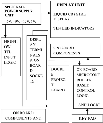
Figure 1:All-in-One Electronics Laboratory (AEL-350) Trainer block diagram.
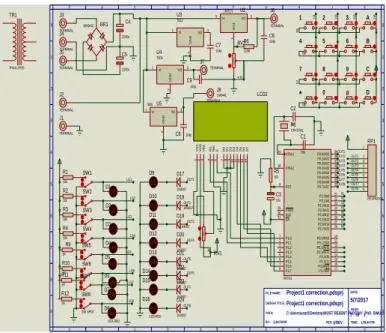
D. The AEL-350 Circuit Diagram
The circuit diagram was designed with Proteus 8.0 Professional. Proteus 8 consists of a single application PDS.EXE. It is the framework or container which hosts all of the functionalities of Proteus. ISIS, ARES, 3DV all open as tabbed windows within this framework and therefore all have access to the common database. Proteus 8 is a single application with many service modules offering different functionalities (schematic capture, PCB layout, etc.). The wrapper that enables all of the various tools to communicate with each other consists of three main parts namely, application framework, common database and live netlist. Figure 2 shows the complete circuit diagram of the AEL-350 Trainer. As shown in Figure 2, the power supply is of dual sources. A detachable 9V battery is fed into the J1-J2 terminal as one of the power sources (top left corner of Figure 2). While a detachable centre tap 15V transformer has its secondary terminals connected to terminals J3, J4 and J5 respectively. SPLIT RAIL POWER SUPPLY UNIT +5V, +9V, +12V, 5V,-9V,-12V VARABLE +1.25V to +21Vdc DISPLAY UNIT LIQUID CRYSTAL DISPLAY
TEN LED INDICATORS SEVEN SEGMENT DISPLAY ON BOARD COMPONENTS HIGH/L OW TTL INPUT LOGIC DOUBL E PROJEC T BOARD ON BOARD MICROCONT ROLLER BASED CONTROL LOGIC AND LOGIC EMULATOR ON BOARD COMPONENTS AND TERMINALS DISPL AY TERMI NALS & ON BOAR D SOCKE TS KEY PAD
International Journal of New Technology and Research (IJNTR) ISSN:2454-4116, Volume-3, Issue-9, September 2017 Pages 108-113
110 www.ijntr.org FILE NAME: BY: DATE: PAGE: Project1 correction.pdsprj 5/7/2017 @AUTHOR A B C D E F G H J K A B C D E F G H J K 0 1 2 3 4 5 6 7 8 9 0 1 2 3 4 5 6 7 8 9
C:\Users\user2\Desktop\MOST RESENT PHDS\MY_PhD_SIMULATION\Project1 correction.pdsprj
PATH:
1of1
REV:@REV TIME: 1:38:44 PM DESIGN TITLE:Project1 correction.pdsprj
LG1 LG2 rs en LG1 LG2 LG3 LG4 h 5 h6 h 7 h8 OUT7 LG3 LG4 LG5 LG6 LG7 LG8 OUT1 OUT2 OUT3 OUT4 OUT5 OUT6 OUT8 OUT8 OUT6 OUT5 OUT4 OUT3 OUT2 OUT1 OUT7 h8 h7 h6 h5 h4 h3 h2 h1 h 4 h 3 h 1 h2 OUT8 OUT7 OUT6 OUT5 OUT4 OUT3 OUT2 OUT1 XTAL2 18 XTAL1 19 ALE 30 EA 31 PSEN 29 RST 9 P0.0/AD039 P0.1/AD138 P0.2/AD237 P0.3/AD336 P0.4/AD435 P0.5/AD534 P0.6/AD633 P0.7/AD732 P2.7/A15 28 P2.0/A821 P2.1/A922 P2.2/A10 23 P2.3/A11 24 P2.4/A12 25 P2.5/A13 26 P2.6/A14 27 P1.0 1 P1.1 2 P1.2 3 P1.3 4 P1.4 5 P1.5 6 P1.6 7 P1.7 8 P3.0/RXD 10 P3.1/TXD11 P3.2/INT0 12 P3.3/INT1 13 P3.4/T014 P3.7/RD 17 P3.6/WRP3.5/T11615 80C51 SW2 SW1 D1 D2 R2 10k D 7 1 4 D 6 1 3 D 5 1 2 D 4 1 1 D 3 1 0 D 2 9 D 1 8 D 0 7 E 6 R W 5 R S 4 V S S 1 V D D 2 V E E 3 LCD2 LM044L * # 1 2 0 8 3 7 9 4 5 6 A B C D D9 2 3 4 5 6 7 8 9 1 RP1 RESPACK-8 SW4 SW3 D3 D4 R3 10k R4 10k SW6 SW5 D5 D6 R9 1R R10 1R SW8 SW-SPDT SW7 D7 D8 LED-RED R11 1R R12 1R D10 D11 D12 D13 D14 D15 D16 LED-RED R1 10k D17 1N4007 D18 1N4007 D19 1N4007 D20 1N4007 D21 1N4007 D22 1N4007 D23 1N4007 D24 1N4007 X1 CRYSTAL C1 33p C2 33p R5 10k C3 10u VI 3 VO2 A D J 1 U2 LM317L 50% RV1 1k J1 TERMINAL J2 TERMINAL J3 TERMINAL J4 TERMINAL J5 TERMINAL TR1 TRAN-2P3S BR1 BRIDGE C4 2200u C5 2200u 50% RV2 4.7k R6 220R J6 TERMINAL C6 104p VI 1 VO3 G N D 2 U3 7812 VI 1 VO3 G N D 2 U4 7809 VI 1 VO3 G N D 2 U5 7805 C7 104p C8 104p C9 104p J7 TERMINAL J8 TERMINAL
Figure 2: Complete Circuit Diagram for AEL-350 (Proteus 8.0 Circuit Simulation and Design).
In Figure 2, BR1 is a bridge rectifier used for voltage rectification while capacitors C4 and C5 are for smoothing the DC voltage. Various voltage regulators both positive and negative were used to regulate voltage levels (U2, U3, U4 and U5). Multiple voltage outputs will enable the Trainer to be useful for various types of experiments. The 5V regulator is used for voltage regulation for the onboard circuit. Another 5V regulator equally provides TTL logic level for the level switches such that logic “1” has TTL high value of 5V and logic “0” value 0V. Eight switches SW1 to SW8 are used for these purposes. They simply switch 5V to the intended destination once they are made, and 0V when unmade. Light Emitting Diodes (LED) D1 to D8 are connected to the terminals of the contact level switches such that they either glow for logic 1 or they stay off for logic 0, also LED D9 to D16 are used as output monitor for circuits. These help in monitoring signal level and drawing truth table in logic gate circuitry.
Figure 3 is a snapshot of the second part of the design exported from Eagle 6.0 Professional. It shows the development board for both ATMEL microcontroller and PIC controller. Unlike the first part of the circuit shown in Figure 2 where an embedded program control the circuit operation, this part of the circuit has no embedded program. It is meant to be manipulated by the user as the used deems fit. An onboard microcontroller and PIC controller with free ports are left to user’s discretion for performing various experiments.
Several displays such as a liquid crystal display, seven segment display and light emitting diodes are onboard. The photograph of the AEL-350 is shown in Figure 4.
Figure 3: Circuit Diagram of Microcontroller Development Board (Snap Shot from Eagle 6.1.o Professional).
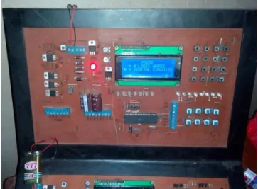
Figure 4: Photo of AEL-350 Trainer. E. AEL-350 Trainer Operation
The upper part of the Trainer shown in Figure 4 is designed for performing experiments by emulation. It has Atmel 8955 Microcontroller; an embedded program burned into it makes possible emulation of digital Integrated Circuit (IC) experiments. All experiments on emulation use the first Liquid Crystal Display. The Keypad on the top right hand side of the Trainer; is the input element for the Microcontroller. Normal contact switches were arranged to form the Keypad. The main advantage of this approach is that each button can be replaced independently without having to change the entire Keypad.
Using the Keypad, various experiments can be performed by emulation. The star button (*) is used to select Logic gate experiments while numbers 1 to 6 are used to select various logic gates. The “#” button is used to select digital circuit experiments while numbers 1 to 7 are used to select various digital circuitries such as RS latches, D, JK flip flop and others.
The lower part of the Trainer is for hardware experiments and for building projects. It contains an LED, breadboard, onboard components and the dual rail power supply.
An Experimentation Framework for Project- Based Learning in Electronics
Various components can be inserted on the breadboard for building circuits or performing experiments. About 350 experiments and projects can be performed to have a very good understanding of electronics.
III. EXPERIMENTS AND TESTS A. Modular Circuit Testing
The AEL-350 Trainer was tested in stages, firstly the simulated circuit was tested through some simulation software namely Proteus 8.0 Professional and Life Wire simulation software. While the circuit diagram was completely designed and tested with Proteus 8.0, the Life Wire simulation software was used alongside Proteus in the test experimentation part of the work. Some observations and test results were made and obtained respectively. These test results are referred here as PROTEUS snaps shots and are shown under the subsequent subsections and figures. Each module was found performing according to design specifications.
B. The Power Supply Module
The power supply module is as important as the control part of this work. This is because it does not only supply the needed power for the Trainer but it also supplies power for the various breadboard experiments both for analogue and digital circuitry. Multiple test instruments like DC Voltmeters, AC Voltmeter and Ammeter were used to ascertain the level of compliance with design specification and objectives. The voltmeter monitored both the input and output voltage sources and necessary adjustment was made to the Proteus design to ensure consistency with design specification.
The input voltages are 220Vac and 18Vdc. While the output voltages were found to be +5V, +9V, +12V, (+1V – +25V variable) and -5V, -9V and -15V negative dc voltages as designed. The +5V supply was replicated thrice to power the onboard circuit while the remaining parts of the power supply was made available for the external experiments. C. Control Logic Test
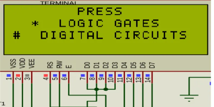
Figure 5 shows the Trainer Liquid Crystal Display in a Proteus snap shot. The simulation showed the control logic is working according to design specification. The embedded C program in the microcontroller uses the Liquid Crystal Display (Figure 5) to present a user friendly interface by asking the user to make choice of either pressing character * for Logic Gate Experiments by Emulation method or to Press # for Digital Circuit Experiments by Emulation Method. FILE NAME: BY: DATE: PAGE: Project1 correction.pdsprj 5/9/2017 @AUTHOR A B C D E F G H J K 1 2 3 4 5 6 7 8 9 1 2 3 4 5 6 7 8 9
C:\Users\user2\Desktop\MOST RESENT PHDS\MY_PhD_SIMULATION\Project1 correction.pdsprj PATH:
1 of 1
REV:@REV TIME: 1:03:49 PM DESIGN TITLE: Project1 correction.pdsprj
LG1 LG2 rs en LG1 LG2 LG3 LG4 h6 h7 h8 OUT7 LG3 LG4 LG5 LG6 LG7 LG8 OUT1 OUT2 OUT3 OUT4 OUT5 OUT6 OUT8 OUT8 OUT6 OUT5 OUT4 OUT3 OUT2 OUT1 OUT7 h8 h7 h6 h5 h4 h3 h2 h1 OUT8 OUT7 OUT6 OUT5 OUT4 OUT3 OUT2 OUT1 XTAL2 18 XTAL1 19 ALE 30 EA 31 PSEN 29 RST 9 P0.0/AD0 39 P0.1/AD1 38 P0.2/AD2 37 P0.3/AD3 36 P0.4/AD4 35 P0.5/AD5 34 P0.6/AD6 33 P0.7/AD7 32 P2.7/A15 28 P2.0/A8 21 P2.1/A9 22 P2.2/A10 23 P2.3/A11 24 P2.4/A12 25 P2.5/A13 26 P2.6/A14 27 P1.0 1 P1.1 2 P1.2 3 P1.3 4 P1.4 5 P1.5 6 P1.6 7 P1.7 8 P3.0/RXD 10 P3.1/TXD 11 P3.2/INT0 12 P3.3/INT1 13 P3.4/T0 14 P3.7/RD 17 P3.6/WR 16 P3.5/T1 15 80C51 SW2 SW1 D1 D2 R2 10k D 7 14 D 6 13 D 5 12 D 4 11 D 3 10 D 2 9 D 1 8 D 0 7 E 6 RW 5 RS 4 VS S 1 VD D 2 VE E 3 LCD2 LM044L
*
0 # 8 7 9 4 5 6 B C D D9 2 3 4 5 6 7 8 9 1 RP1 RESPACK-8 SW4 SW3 D3 D4 R3 10k R4 10k SW6 SW5 D5 D6 R9 1R R10 1R SW8 SW -SPDT SW7 D7 D8 LED-RED R11 1R R12 1R D10 D11 D12 D13 D14 D15 D16 LED-RED R1 10k D17 1N4007 D18 1N4007 D19 1N4007 D20 1N4007 D21 1N4007 D22 1N4007 D23 1N4007 D24 1N4007 X1 CRYSTAL C1 33p C2 33p R5 10k C3 10u 1 50 % RV1 1k J1 TERMINAL J2 TERMINAL TERMINAL J5 TERMINAL TRAN-2P3S 2200u C5 2200u 50 % RV2 4.7k R6 220R C6 104p G N D 2 VI 1 VO 3 G N D 2 U4 7809 VI 1 VO 3 G N D 2 U5 7805 C7 104p C8 104p C9 104p J7 TERMINAL J8 TERMINALFigure 5: Trainer Liquid Crystal Display (Proteus
Snapshot).
D. Logic Gate Experiments
Figure 6 and Figure 7 show Proteus Snapshot for Logic gate Experiments. While the entire Control Logic Circuit is shown in Figure 6, only the LCD interface was shown in Figure 7. These Snapshots were the result obtained by selecting the * button on the key pad as requested in Figure 5 above. FILE NAME: BY: DATE: PAGE: Project1 correction.pdsprj 5/9/2017 @AUTHOR B C D E F G H J K A B C D E F G H J K
C:\Users\user2\Desktop\MOST RESENT PHDS\MY_PhD_SIMULATION\Project1 correction.pdsprj PATH: 1of1
REV:@REV TIME:1:13:49 PM DESIGN TITLE:Project1 correction.pdsprj
LG1 LG2 rs en LG1 LG2 LG3 LG4 h 5 h6 h 7 h8 OUT7 LG3 LG4 LG5 LG6 LG7 LG8 OUT1 OUT2 OUT3 OUT4 OUT5 OUT6 OUT8 OUT8 OUT6 OUT5 OUT4 OUT3 OUT2 OUT1 OUT7 h8 h7 h6 h5 h4 h3 h2 h1 h 4 h 3 h 1 h2 OUT8 OUT7 OUT6 OUT5 OUT4 OUT3 OUT2 OUT1 XTAL2 18 XTAL1 19 ALE 30 EA 31 PSEN 29 RST 9 P0.0/AD0 39 P0.1/AD1 38 P0.2/AD2 37 P0.3/AD3 36 P0.4/AD4 35 P0.5/AD5 34 P0.6/AD6 33 P0.7/AD7 32 P2.7/A15 28 P2.0/A8 21 P2.1/A9 22 P2.2/A10 23 P2.3/A11 24 P2.4/A12 25 P2.5/A13 26 P2.6/A14 27 P1.0 1 P1.1 2 P1.2 3 P1.3 4 P1.4 5 P1.5 6 P1.6 7 P1.7 8 P3.0/RXD 10 P3.1/TXD 11 P3.2/INT0 12 P3.3/INT1 13 P3.4/T0 14 P3.7/RD 17 P3.6/WRP3.5/T1 1615 80C51 SW2 SW1 D1 D2 R2 10k D 7 1 4 D 6 1 3 D 5 1 2 D 4 11 D 3 1 0 D 2 9 D 1 8 D 0 7 E 6 R W 5 R S 4 V S S 1 V D D 2 V E E 3 LCD2 LM044L * # 1 2 0 8 3 7 9 4 5 6 A B C D D9 2 3 4 5 6 7 8 9 1 RP1 RESPACK-8 SW4 SW3 D3 D4 R3 10k R4 10k SW6 SW5 D5 D6 R9 1R R10 1R SW8 SW -SPDT SW7 D7 D8 LED-RED R11 1R R12 1R D10 D11 D12 D13 D14 D15 D16 LED-RED R1 10k D17 1N4007 D18 1N4007 D19 1N4007 D20 1N4007 D21 1N4007 D22 1N4007 D23 1N4007 D24 1N4007 X1 CRYSTAL C1 33p C2 33p R5 10k C3 10u VI 3 VO 2 A D J 1 U2 LM317L 5 0% RV1 1k J1 TERMINAL J2 TERMINAL J3 TERMINAL J4 TERMINAL J5 TERMINAL BR1 BRIDGE C4 2200u C5 2200u 50% RV2 4.7k R6 220R J6 TERMINAL C6 104p VI 1 VO 3 G N D 2 U3 7812 VI 1 VO 3 G N D 2 U4 7809 VI 1 VO 3 G N D 2 U5 7805 C7 104p C8 104p C9 104p J7 TERMINAL J8 TERMINAL
Figure 6: Logic Gate Experiments by Emulation (Proteus Snapshot). A B C D E F G H J K 0 1 2 3 4 5 6 7 0 1 2 3 4 5 6 7 LG1 LG2 rs en LG1 LG2 LG3 LG4 en rs OUT1 LG3 LG4 LG5 LG6 LG7 LG8 OUT1 OUT2 OUT3 OUT4 OUT5 OUT6 OUT7 OUT8 OUT2 OUT3 OUT4 OUT5 OUT6 OUT7 OUT8 OUT8 OUT7 OUT6 OUT5 OUT4 OUT3 OUT2 OUT1 XTAL2 18 XTAL1 19 ALE 30 EA 31 PSEN 29 RST 9 P0.0/AD0 39 P0.1/AD1 38 P0.2/AD2 37 P0.3/AD3 36 P0.4/AD4 35 P0.5/AD5 34 P0.6/AD6 33 P0.7/AD7 32 P2.7/A15 28 P2.0/A8 21 P2.1/A9 22 P2.2/A10 23 P2.3/A11 24 P2.4/A12 25 P2.5/A13 26 P2.6/A14 27 P1.0 1 P1.1 2 P1.2 3 P1.3 4 P1.4 5 P1.5 6 P1.6 7 P1.7 8 P3.0/RXD 10 P3.1/TXD 11 P3.2/INT0 12 P3.3/INT1 13 P3.4/T0 14 P3.7/RD 17 P3.6/W RP3.5/T1 16 15 80C51 SW1 SW -SPDT SW3 SW -SPDT D1 LED-RED D2 LED-RED R2 10k D7 14 D6 13 D5 12 D4 11 D3 10 D2 9 D1 8 D0 7 E 6 RW 5 RS 4 VS S 1 VD D 2 VE E 3 LCD2 LM044L * # 1 2 0 8 3 7 9 4 5 6 A B C D D5 LED-RED 2 3 4 5 6 7 8 9 1 RP1 RESPACK-8 SW2 SW -SPDT SW4 SW -SPDT D3 LED-RED D4 LED-RED R3 10k R4 10k SW5 SW -SPDT SW6 SW -SPDT D6 LED-RED D7 LED-RED R9 1R R10 1R SW7 SW -SPDT SW8 SW -SPDT D8 LED-RED D9 LED-RED R11 1R R12 1R D10 LED-RED D11 LED-RED D13 LED-RED D12 LED-RED D14 LED-RED D15 LED-RED D16 LED-RED R1
10k Figure 7: LCD Interface for Logic Gate Experiments by
Emulation (Proteus Snapshot).
As implied by the liquid crystal display, the user is given six experiment options
Press 1 for OR gate experiment by Emulation Press 2 for AND gate Experiment by Emulation Press 3 for XOR gate Experiment by Emulation Press 4 for NOR gate Experiment by Emulation
International Journal of New Technology and Research (IJNTR) ISSN:2454-4116, Volume-3, Issue-9, September 2017 Pages 108-113
112 www.ijntr.org
Press 5 for NAND Gate Experiment by Emulation Method Press 6 for XNOR Gate Experiment by Emulation Method E. Digital Circuit (Flip Flop) Experiments
On the other hand, selecting the # button gives the user the other option for digital circuit and flip-flop experiments. This is exemplified by the device read out as shown in Figure 8 and Figure 9
FILE NAME: BY: DATE: PAGE: Project1 correction.pdsprj 5/9/2017 @AUTHOR A B C D E F G H J K A B C D E F G H J K
C:\Users\user2\Desktop\MOST RESENT PHDS\MY_PhD_SIMULATION\Project1 correction.pdsprj PATH: 1of1
REV:@REV TIME:1:13:49 PM DESIGN TITLE:Project1 correction.pdsprj
LG1 LG2 rs en LG1 LG2 LG3 LG4 h 5 h6 h 7 h8 OUT7 LG3 LG4 LG5 LG6 LG7 LG8 OUT1 OUT2 OUT3 OUT4 OUT5 OUT6 OUT8 OUT8 OUT6 OUT5 OUT4 OUT3 OUT2 OUT1 OUT7 h8 h7 h6 h5 h4 h3 h2 h1 h4 h3 h1 h2 OUT8 OUT7 OUT6 OUT5 OUT4 OUT3 OUT2 OUT1 XTAL2 18 XTAL1 19 ALE 30 EA 31 PSEN 29 RST 9 P0.0/AD0 39 P0.1/AD1 38 P0.2/AD2 37 P0.3/AD3 36 P0.4/AD4 35 P0.5/AD5 34 P0.6/AD6 33 P0.7/AD7 32 P2.7/A1528 P2.0/A821 P2.1/A922 P2.2/A1023 P2.3/A1124 P2.4/A1225 P2.5/A1326 P2.6/A1427 P1.0 1 P1.1 2 P1.2 3 P1.3 4 P1.4 5 P1.5 6 P1.6 7 P1.7 8 P3.0/RXD10 P3.1/TXD 11 P3.2/INT012 P3.3/INT113 P3.4/T014 P3.7/RD17 P3.6/WRP3.5/T11615 80C51 SW2 SW1 D1 D2 R2 10k D 7 14 D 6 13 D 5 12 D 4 11 D 3 10 D 2 9 D 1 8 D 0 7 E 6 R W 5 R S 4 V S S 1 V D D 2 V E E 3 LCD2 LM044L * # 1 2 0 8 3 7 9 4 5 6 A B C D D9 2 3 4 5 6 7 8 9 1 RP1 RESPACK-8 SW4 SW3 D3 D4 R3 10k R4 10k SW6 SW5 D5 D6 R9 1R R10 1R SW8 SW -SPDT SW7 D7 D8 LED-RED R11 1R R12 1R D10 D11 D12 D13 D14 D15 D16 LED-RED R1 10k D17 1N4007 D18 1N4007 D19 1N4007 D20 1N4007 D21 1N4007 D22 1N4007 D23 1N4007 D24 1N4007 X1 CRYSTAL C1 33p C2 33p R5 10k C3 10u VI 3 VO2 A D J 1 U2 LM317L 50 % RV1 1k J1 TERMINAL J2 TERMINAL J3 TERMINAL J4 TERMINAL J5 TERMINAL BR1 BRIDGE C4 2200u C5 2200u 50% RV2 4.7k R6 220R J6 TERMINAL C6 104p VI 1 VO 3 G N D 2 U3 7812 VI 1 VO3 G N D 2 U4 7809 VI 1 VO3 G N D 2 U5 7805 C7 104p C8104p C9 104p J7 TERMINAL J8 TERMINAL
Figure 8: Digital Circuit Experiment by Simulation (Proteus Snap Shot). FILE NAME: BY: DATE: PAGE: Project1 correction.pdsprj 5/9/2017 @AUTHOR A B C D E F G H J K A B C D E F G H J K
C:\Users\user2\Desktop\MOST RESENT PHDS\MY_PhD_SIMULATION\Project1 correction.pdsprj PATH:
1of1 REV:@REV TIME: 1:13:49 PM DESIGN TITLE:Project1 correction.pdsprj
LG1 LG2 rs en LG1 LG2 LG3 LG4 h5 h6 h 7 h8 OUT7 LG3 LG4 LG5 LG6 LG7 LG8 OUT1 OUT2 OUT3 OUT4 OUT5 OUT6 OUT8 OUT8 OUT6 OUT5 OUT4 OUT3 OUT2 OUT1 OUT7 h8 h7 h6 h5 h4 h3 h2 h1 h 4 h 3 h 1 h2 OUT8 OUT7 OUT6 OUT5 OUT4 OUT3 OUT2 OUT1 XTAL2 18 XTAL1 19 ALE 30 EA 31 PSEN 29 RST 9 P0.0/AD039 P0.1/AD138 P0.2/AD237 P0.3/AD336 P0.4/AD435 P0.5/AD534 P0.6/AD633 P0.7/AD732 P2.7/A15 28 P2.0/A821 P2.1/A922 P2.2/A10 23 P2.3/A11 24 P2.4/A12 25 P2.5/A13 26 P2.6/A14 27 P1.0 1 P1.1 2 P1.2 3 P1.3 4 P1.4 5 P1.5 6 P1.6 7 P1.7 8 P3.0/RXD 10 P3.1/TXD11 P3.2/INT0 12 P3.3/INT1 13 P3.4/T0 14 P3.7/RD 17 P3.6/WRP3.5/T1 1615 80C51 SW2 SW1 D1 D2 R2 10k D 7 1 4 D 6 1 3 D 5 1 2 D 4 11 D 3 1 0 D 2 9 D 1 8 D 0 7 E 6 R W 5 R S 4 V S S 1 V D D 2 V E E 3 LCD2 LM044L * # 1 2 0 8 3 7 9 4 5 6 A B C D D9 2 3 4 5 6 7 8 9 1 RP1 RESPACK-8 SW4 SW3 D3 D4 R3 10k R4 10k SW6 SW5 D5 D6 R9 1R R10 1R SW8 SW-SPDT SW7 D7 D8 LED-RED R11 1R R12 1R D10 D11 D12 D13 D14 D15 D16 LED-RED R1 10k D17 1N4007 D18 1N4007 D19 1N4007 D20 1N4007 D21 1N4007 D22 1N4007 D23 1N4007 D24 1N4007 X1 CRYSTAL C1 33p C2 33p R5 10k C3 10u VI 3 VO 2 A D J 1 U2 LM317L 50% RV1 1k J1 TERMINAL J2 TERMINAL J3 TERMINAL J4 TERMINAL J5 TERMINAL BR1 BRIDGE C4 2200u C5 2200u 50% RV2 4.7k R6 220R J6 TERMINAL C6 104p VI 1 VO3 G N D 2 U3 7812 VI 1 VO 3 G N D 2 U4 7809 VI 1 VO 3 G N D 2 U5 7805 C7 104p C8104p C9 104p J7 TERMINAL J8 TERMINAL
Figure 9: Digital Circuit Experiment by Simulation (Proteus
Snap Shot).
The interface gave 5 experiment options namely: D Flip Flop, JK Flip Flop,SR Flip Flop, Decoder and Encoder. To perform any of these experiments, the corresponding number must be selected on the Keypad. Following the steps above, the equipment successfully performed numerous logic gates and other electronics experiments.
IV. RESULTS AND DISCUSSION
The forgoing has been the Proteus snapshots to prove the correctness of the design. The actual photograph of the
upper part of AEL-350 designed for experimentation by emulation (performing experiments without components) is shown in Figure 10 with the equipment powered on.
Figure 10: Photograph of upper Section of AEL-350 when powered on.
The lower part, Figure 11, has all the necessary components found on microcontroller boards and more. Various types of microcontroller based projects can be carried out on this section.
Figure 11: The Microcontroller Board Section. A user can perform digital systems experiments severally to enable the user have very good understanding without the use of the actual components. Thereafter, he or she can now build actual circuits on the breadboard on the Lower section. The AEL-350 equipment is rugged and affordable so that institutions can purchase many modules for their labs. Additionally, hobbyists and individual students can also buy it for themselves. A pilot study carried out with a technical school revealed that at the end of the semester, majority of
the students demonstrated a good understanding in designing and building circuits.
As a Microcontroller board, the AEL-350 user is at liberty to use desired port of the microcontroller to drive any of the displays. This flexibility is made possible by terminating the microcontroller’s ports and the display ports on sets of well labeled sockets, such that jumper wires are used for external connection. Unlike most other trainers, this opportunity to determine the port assignment as the user deems fit is an added advantage that will enable the user get very versatile with the microcontrollers. Besides this, the very fact that IC sockets were used onboard will also enable the use of many other highly compatible microcontrollers with this development board.
V. CONCLUSION AND RECOMMENDATIONS A. Conclusion
A comprehensive but handy multipurpose electronics laboratory trainer has been carefully developed as a viable framework for project-based learning in the field of electronics. Almost every kind of analogue, digital and opto-electronics experiments can be carried out using the equipment. The Trainer incorporates both hardware and embedded software. The hardware was designed according to the project objectives and specifications. While necessary components calculations were made, the manufacturer’s data sheet was consulted to ascertain the parameters of some specific components. The Microcontroller used was programmed using embedded C language. This however was used primarily for the control logic. Circuits were tested and simulated with Proteus 8.0 and Eagle Professionals Simulation software. The printed circuit board was developed primarily with Eagle 6.1.0 simulation software. An additional simulation software called Lifewire was used for developing the practical handbook.
B. Recommendations
In other to drive home the objectives of this work and the problems it intended to solve, the following recommendations are thus made.
a) That some relevant curriculum on electronics be redeveloped to follow project-based delivery approach for enhanced practical knowhow and effective learning. b) That the equipment be further improved to make it
smaller in size.
C. Contribution to Knowledge
An experimentation platform as a solution to the noticeable deficiency in practical know-how has been developed with multiple experimentation capability. AEL-350 is simpler and cheaper than the other trainers in the market. To ensure proper mastery of electronics design, a tutorial/manual is developed for the Trainer. Finally, AEL-350 is an indigenous design that will definitely have the designer
within reach with the parts readily made available for maintenance purposes.
REFERENCES
[1] A handbook for middle and high school teachers. Novato, CA: The Buck Institute for Education
[2] Blumenfeld, P., Soloway, E., Marx, R., Krajcik, J., Guzdial, M., & Palincsar, A. (1991). Motiva ting project-based learning: Sustaining the doing, supporting the learning. Educational Psychologist, 26 (3&4), 369-398.
[3] Boaler, J. (1997). Experiencing school mathematics; Teaching styles, sex, and settings. Buckingham, UK: Open University Press
[4] Diehl, W., Grobe, T., Lopez, H., & Cabral, C. (1999). Project-based learning: A strategy for teaching and learning. Boston, MA: Center for Youth Development and Education, Corporation for Business, Work, and Learning. Education.
[5] George Lucas Educational Foundation. (2001, November 1). Project-based learning research. Edutopia. www.edutopia.org* International Society for Technology in Education.
[6] Jones, B. F., Rasmussen, C. M., & Moffitt, M. C. (1997). Real-life problem solving.: A collaborative approach to interdisciplinary learning. Washington, DC: American Psychological Association.
[7] Moursund, D. (1999). Project-based learning using information technology. Eugene, OR:
[8] Railsback, J. (2002). Project-based instruction: Creating excitement for learning. Portland, OR: Northwest Regional Educational Laboratory. http://www.nwrel.org/request/2002aug/index.html
[9] San Rafael, Autodesk Foundation (1999). Kids who know and do--1999. Program for the 7th Annual San Conference on Project-Based Learning, San Francisco. San Rafael:
[10] SRI International. (2000, January). Silicon valley challenge 2000: Year 4 Report. San Jose, CA: Joint Venture, Silicon Valley Network. http://pblmm.k12.ca.us/sri/Reports.htm*
[ [11] Thomas, J. W., Mergendoller, J. R., and Michaelson, A. (1999). Project-based learning:
[12] Thomas, J.W. (1998). Project-based learning: Overview. Novato, CA: Buck Institute for Education
[ [13] Thomas, J.W. (2000). A review of research on project-based learning. San Rafael, CA: Autodesk. http://www.k12reform.org/foundation/pbl/research