Fujitsu Microelectronics Europe
Application Note
MCU-AN-300104-E-V10FR FAMILY
32-BIT MICROCONTROLLER
MB91460
CLOCK SUPERVISOR
APPLICATION NOTE
CLOCK SUPERVISOR Revision History
Revision History
Date Issue 2008-06-18 V1.0, First draft, HPi
CLOCK SUPERVISOR Warranty and Disclaimer
Warranty and Disclaimer
To the maximum extent permitted by applicable law, Fujitsu Microelectronics Europe GmbH restricts its warranties and its liability for all products delivered free of charge (eg. software include or header files, application examples, target boards, evaluation boards, engineering samples of IC’s etc.), its performance and any consequential damages, on the use of the Product in accordance with (i) the terms of the License Agreement and the Sale and Purchase Agreement under which agreements the Product has been delivered, (ii) the technical descriptions and (iii) all accompanying written materials. In addition, to the maximum extent permitted by applicable law, Fujitsu Microelectronics Europe GmbH disclaims all warranties and liabilities for the performance of the Product and any consequential damages in cases of unauthorised decompiling and/or reverse engineering and/or disassembling. Note, all these products are intended and must only be used in an evaluation laboratory environment.
1. Fujitsu Microelectronics Europe GmbH warrants that the Product will perform substantially in accordance with the accompanying written materials for a period of 90 days form the date of receipt by the customer. Concerning the hardware components of the Product, Fujitsu Microelectronics Europe GmbH warrants that the Product will be free from defects in material and workmanship under use and service as specified in the accompanying written materials for a duration of 1 year from the date of receipt by the customer.
2. Should a Product turn out to be defect, Fujitsu Microelectronics Europe GmbH´s entire liability and the customer´s exclusive remedy shall be, at Fujitsu Microelectronics Europe GmbH´s sole discretion, either return of the purchase price and the license fee, or replacement of the Product or parts thereof, if the Product is returned to Fujitsu Microelectronics Europe GmbH in original packing and without further defects resulting from the customer´s use or the transport. However, this warranty is excluded if the defect has resulted from an accident not attributable to Fujitsu Microelectronics Europe GmbH, or abuse or misapplication attributable to the customer or any other third party not relating to Fujitsu Microelectronics Europe GmbH.
3. To the maximum extent permitted by applicable law Fujitsu Microelectronics Europe GmbH disclaims all other warranties, whether expressed or implied, in particular, but not limited to, warranties of merchantability and fitness for a particular purpose for which the Product is not designated.
4. To the maximum extent permitted by applicable law, Fujitsu Microelectronics Europe GmbH´s and its suppliers´ liability is restricted to intention and gross negligence.
NO LIABILITY FOR CONSEQUENTIAL DAMAGES
To the maximum extent permitted by applicable law, in no event shall Fujitsu Microelectronics Europe GmbH and its suppliers be liable for any damages whatsoever (including but without limitation, consequential and/or indirect damages for personal injury, assets of substantial value, loss of profits, interruption of business operation, loss of information, or any other monetary or pecuniary loss) arising from the use of the Product.
Should one of the above stipulations be or become invalid and/or unenforceable, the remaining stipulations shall stay in full effect
CLOCK SUPERVISOR Contents
Contents
REVISION HISTORY ... 2
WARRANTY AND DISCLAIMER ... 3
CONTENTS ... 4
1 INTRODUCTION... 5
2 CLOCK SUPERVISOR ... 6
2.1 Overview ... 6
2.2 Registers... 7
2.2.1 Clock Supervisor Control Register (CSVCR) ... 7
2.3 Operation Modes... 8
2.3.1 Operation mode with initial settings ... 8
2.3.2 Disabling the RC-oscillator and the clock supervisors... 8
2.3.3 Re-enabling the RC-oscillator and the clock supervisors ... 8
2.3.4 Clock Supervisor in STOP state... 9
3 CLOCK SUPERVISOR EXAMPLE ... 10
3.1 Enabling and Disabling RC Oscillator ... 10
3.2 Enabling and Disabling Main Clock and Sub Clock Supervisor... 10
4 ADDITIONAL INFORMATION ... 11
CLOCK SUPERVISOR Chapter 1 Introduction
1 Introduction
This application note gives an overview of the Clock Supervisor.
Purpose of the Clock Supervisor is the supervision of the Main and Sub oscillators. In case of oscillation (OSCMAIN or OSCSUB) failure the Clock Supervisor control logic will take action, i.e. switching to an internal RC-oscillation clock (CLKRC 100 kHz), depending on the operation mode set in the control register.
CLOCK SUPERVISOR Chapter 2 Clock Supervisor
2 Clock Supervisor
This chapter explains the Clock Supervisor in detail.
2.1 Overview
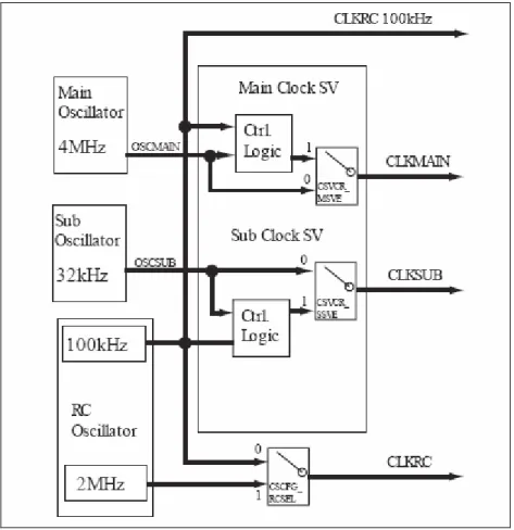
There are two independent supervisors one for the Main clock and one for the Sub clock. They can be enabled/ disabled separately.
Main clock and Sub clock supervisor are disabled and re-enabled automatically if the corresponding oscillator is disabled and re-enabled.
There are two status bits in the Clock Supervisor Control Register which indicate the failure of the Main clock and Sub clock. These bits can be available at two port pins (device dependent).
If a clock used by MCU fails for a certain time (20-80Cs for Main clock / 160-640Cs for Sub clock) the MCU is reset and the reset cause can be checked after reset vector fetch.
To find out whether the Clock Supervisor has asserted reset, the software must check the reset cause by reading the RSRR register. If INIT (bit 7 of RSRR) is set, the cause was either external reset at the INITX pin or the clock supervisor. If neither SM bit nor MM bit (bit 5 and bit 6 of CSVCR) is set, reset cause was the external reset. If SM is ’1’ the reset cause is a missing Sub clock and if MM is ’1’ the reset cause is a missing Main clock.
CLOCK SUPERVISOR Chapter 2 Clock Supervisor
2.2 Registers
This section lists the Clock Supervisor Control Register and describes the function of each bit in detail.
2.2.1 Clock Supervisor Control Register (
CSVCR
)
The Clock Supervisor Control Register (CSVCR) sets the operation mode of the Clock Supervisor.
Bit No. Name Explanation Initial Value
Value Operation
0 Do not enable ports for MCLK_MISSING and SCLK_MISSING output pins
0 OUTE Output enable* 0
1 Enable ports for MCLK_MISSING and
SCLK_MISSING output pins 0
Do not perform reset upon transition from Main clock to Sub clock modes if Sub clock is already missing
1 SRST Sub clock mode reset 0
1
Perform reset upon transition from Main clock to Sub clock modes if Sub clock is already missing
0 Disable Sub clock supervisor
2 SSVE Sub clock supervisor enable 1 1 Enable Sub clock supervisor
0 Disable Main clock supervisor
3 MSVE Main clock supervisor enable 1 1 Enable Main clock supervisor
0 Disable RC-oscillator
4 RCE RC oscillator enable 1 1 Enable RC-oscillator
0 Missing Sub clock has not been detected
5 SM Sub clock missing 0
1 Missing Sub clock has been detected 0 Missing Main clock has not been detected
6 MM Main clock missing 0
1 Missing Main clock has been detected 0 32k oscillation used as Sub clock 7 SCKS Sub clock select (only used for single clock
devices) 0 1 RC oscillation used as Sub clock
Note: This bit can be used as an output enable to output the signals MCLK_MISSING (bit 3 of CSVCR) and SCLK_MISSING (bit 4 of CSVCR) to port pins. For MB9F1460D series it is
available at Pin number 3 and 2 respectively.
CLOCK SUPERVISOR Chapter 2 Clock Supervisor
2.3 Operation
Modes
2.3.1 Operation mode with initial settings
In case the clock supervisor control register (CSVCR) is not configured at the beginning of the user program, the RC-oscillator, the Main clock supervisor and the Sub clock supervisor is enabled.
The Main clock supervisor is enabled after the ‘oscillation stabilization wait time’ or in case the Main clock is missing before the completion of the ‘oscillation stabilization wait time’, after the ‘Main clock timeout’ (TO_MCLK) from the timeout counter. (The timeout counter is clocked with CLKRC) If the Main clock is missing from power-on, the power-on reset state is never left, which in this case is a safe state. The user must make sure with external pull-up/pull-down resistors that all relevant signals are pulled to the correct level.
The Sub clock supervisor is enabled after the completion of the ‘Sub clock timeout’ (TO_SCLK) from the timeout counter.
If the Main clock stops while the Main clock supervisor is enabled, the Main clock is replaced with CLKRC 100kHz, the MM bit is set to ‘1’ and reset (EXT_RST_OUT) is asserted.
If the Sub clock stops and if the Sub clock supervisor is enabled, the behavior depends on whether the MCU is in Main clock mode or in Sub clock mode. If the Sub clock stops in Sub clock mode, CLKRC divided by two substitutes the Sub clock, the SM bit is set to ‘1’ and reset (EXT_RST_OUT) is asserted. If the Sub clock stops in Main clock mode, CLKRC divided by two substitutes the Sub clock, the SM bit is set to ‘1’ and no reset occurs upon transition to Sub clock mode, since the SRST bit has its initial value of ’0’. If the SRST bit is ‘1’ a reset (INIT) occurs
2.3.2 Disabling the RC-oscillator and the clock supervisors
The RC-oscillator can be disabled by setting bit RCE (bit 4 of CSVCR) to ’0’.
First disable the Main clock and Sub clock supervisor. Do not disable the RC-oscillator while either the Main clock or Sub clock supervisor is still enabled. Then check that both SM and MM (bit 5 and bit 6 of CSVCR) are still ‘0’. Disable the RC oscillator by setting RCE to ‘0’. If either SM or MM bit is ‘1’, RCE must not be set to ‘0’.
The Main clock supervisor is disabled by setting MSVE (bit 3 of CSVCR) to ‘0’. The Sub clock supervisor is disabled by setting SSVE (bit 2 of CVSVR) to ‘0’.
2.3.3 Re-enabling the RC-oscillator and the clock supervisors
The RC-oscillator can be enabled by setting RCE (bit 4 of CSVCR) to ‘1’.
The Main clock supervisor is enabled by setting MSVE (bit 3 of CSVCR) to ‘1’. Enabling of the Main clock supervisor must only take place 100Cs after the RC-oscillator is enabled. The software has to take care that this time constraint is met.
The Sub clock supervisor is enabled by setting SSVE (bit 2 of CSVCR) to ‘1’. Enabling of the Sub clock supervisor must only take place 100Cs after the RC-oscillator is enabled. The software has to take care that this time constraint is met.
CLOCK SUPERVISOR Chapter 2 Clock Supervisor
2.3.4 Clock Supervisor in STOP state
If RC-oscillator, Main clock and Sub clock supervisors are automatically disabled at transition into STOP state if they are enabled already. The corresponding enable bits in the clock supervisor control register remain unchanged. So after wake-up from STOP state the RC-oscillator and the clock supervisors will be enabled again.
If the corresponding enable bits are set to ‘0’, the RC-oscillator and the clock supervisors will stay disabled after wake-up from STOP state.
The RC-oscillator is enabled immediately after wake-up from STOP state.
The Main clock supervisor is enabled after the ‘oscillation stabilization wait time’ or in case the Main clock is missing after wake-up from STOP state, after the ‘Main clock timeout’ (TO_MCLK) from the timeout counter which is clocked with the CLKRC.
The Sub clock supervisor is enabled after the ‘Sub clock timeout’ (TO_SCLK) from the timeout counter which is clocked with the CLKRC.
CLOCK SUPERVISOR Chapter 3 Clock Supervisor Example
3 Clock Supervisor Example
EXAMPLE FOR CLOCK SUPERVISOR3.1 Enabling and Disabling RC Oscillator
3.2 Enabling and Disabling Main Clock and Sub Clock Supervisor
/* THIS SAMPLE CODE IS PROVIDED AS IS AND IS SUBJECT TO ALTERATIONS. FUJITSU */ /* MICROELECTRONICS ACCEPTS NO RESPONSIBILITY OR LIABILITY FOR ANY ERRORS OR */ /* ELIGIBILITY FOR ANY PURPOSES. */ /* (C) Fujitsu Microelectronics Europe GmbH */ /*---
char Set_RCE(char state){
if (state) {
CSVCR_RCE = 1; /* Enable RC Oscillator */ } else {
CSVCR_MSVE = 0; /* Disable Clock supervisor */ CSVCR_SSVE = 0;
while (CSVCR_SM == 1 || CSVCR_MM == 1){ HWWD = 0;
}
CSVCR_RCE = 0; /*Disable RC Oscillator */ }
return 0; }
/* THIS SAMPLE CODE IS PROVIDED AS IS AND IS SUBJECT TO ALTERATIONS. FUJITSU */ /* MICROELECTRONICS ACCEPTS NO RESPONSIBILITY OR LIABILITY FOR ANY ERRORS OR */ /* ELIGIBILITY FOR ANY PURPOSES. */ /* (C) Fujitsu Microelectronics Europe GmbH */ /*---
char Set_MSVE(char state){ /*Enable Main clock supervisor*/
if (state) CSVCR_MSVE = 1; else CSVCR_MSVE = 0; return 0; }
char Set_SSVE(char state){ /*Enable Sub clock supervisor*/
if (state) CSVCR_SSVE = 1; else CSVCR_SSVE = 0; return 0; }
CLOCK SUPERVISOR Chapter 4 Additional Information
4 Additional Information
Information about FUJITSU Microcontrollers can be found on the following Internet page: http://mcu.emea.fujitsu.com/
The software examples related to this application note is:
91460_ClockSupervisor
It can be found on the following Internet page:
CLOCK SUPERVISOR List of Figures