Porto Institutional Repository
[Doctoral thesis] Energy-efficient hardware design based on high-level
synthesis
Original Citation:
Muslim, Fahad Bin (2017). Energy-efficient hardware design based on high-level synthesis. PhD thesis
Availability:
This version is available at :http://porto.polito.it/2666504/since: March 2017 Published version:
DOI:10.6092/polito/porto/2666504
Terms of use:
This article is made available under terms and conditions applicable to Open Access Policy Article ("Public - All rights reserved") , as described athttp://porto.polito.it/terms_and_conditions. html
Porto, the institutional repository of the Politecnico di Torino, is provided by the University Library and the IT-Services. The aim is to enable open access to all the world. Pleaseshare with ushow this access benefits you. Your story matters.
Doctoral Dissertation
Doctoral Program in Electronics Engineering (29thcycle)
Energy-efficient hardware design
based on high-level synthesis
By
Fahad Bin Muslim
******
Supervisor(s):
Prof. Luciano Lavagno, Supervisor
Doctoral Examination Committee:
Prof. Roberto Guerrieri, Universita’ di Bologna Prof. Antonio Abramo, Universita’ di Udine Ing. Davide Quaglia, Universita’ di Verona Prof. Leonardo Reyneri, Politecnico di Torino Prof. Claudio Passerone, Politecnico di Torino
Politecnico di Torino 2017
Declaration
I hereby declare that, the contents and organization of this dissertation constitute my own original work and does not compromise in any way the rights of third parties, including those relating to the security of personal data.
Fahad Bin Muslim 2017
* This dissertation is presented in partial fulfillment of the requirements forPh.D. degreein the Graduate School of Politecnico di Torino (ScuDo).
Acknowledgements
First and foremost, I would like to thank Allah-the Almighty for all His blessings bestowed upon me. Without His will, I would not have made it this far.
I would like to express a special gratitude to my supervisor and mentor Prof. Luciano Lavagno for the excellent ideas that he proposed for me to work on. The work was challenging but it was through his commendable guidance which enabled me to get some useful results eventually. He was always there to address my work-related as well as other general queries even with his extremely busy schedule. Besides, I would like to thank all the faculty members and researchers from the department of electronics and telecommunications (DET) at Politecnico di Torino, who supported me in any way during the course of my PhD.
I would also like to thank my several friends that I made during my stay here in Turin for making my stay extremely pleasant and memorable. I would also like to take this opportunity to acknowledge the support of my group mates (past and present) at the High-level synthesis group at Polito. The discussions with them have always been extremely rewarding and I learnt a lot from them.
A special word of appreciation for my family members including my parents, wife, siblings and others for their unconditional support and prayers. They always had extremely encouraging words for me especially, when the chips were down.
Finally, I am extremely thankful to the higher education commission (HEC) Pakistan for funding my doctorate at the Politecnico di Torino. This is a great initiative by the government of Pakistan to create a pool of high quality researchers who can ultimately contribute to the prosperity of the nation. I find myself more equipped after my PhD to contribute to this goal.
Abstract
This dissertation describes research activities broadly concerning the area of High-level synthesis (HLS), but more specifically, regarding the HLS-based design of energy-efficient hardware (HW) accelerators. HW accelerators, mostly implemented on FPGAs, are integral to the heterogeneous architectures employed in modern high performance computing (HPC) systems due to their ability to speed up the execution while dramatically reducing the energy consumption of computationally challenging portions of complex applications. Hence, the first activity was regarding an HLS-based approach to directly execute an OpenCL code on an FPGA instead of its traditional GPU-based counterpart. Modern FPGAs offer considerable computational capabilities while consuming significantly smaller power as compared to high-end GPUs. Several different implementations of the K-Nearest Neighbor algorithm were considered on both FPGA- and GPU-based platforms and their performance was compared. FPGAs were generally more energy-efficient than the GPUs in all the test cases. Eventually, we were also able to get a faster (in terms of execution time) FPGA implementation by using an FPGA-specific OpenCL coding style and utilizing suitable HLS directives.
The second activity was targeted towards the development of a methodology complementing HLS to automatically derive power optimization directives (also known as "power intent") from a system-level design description and use it to drive the design steps after HLS, by producing a directive file written using the common power format (CPF) to achieve power shut-off (PSO) in case of an ASIC design. The proposed LP-HLS methodology reduces the design effort by enabling designers to infer low power information from the system-level description of a design rather than at the RTL. This methodology required a SystemC description of a generic power management module to describe the design context of a HW module also modeled in SystemC, along with the development of a tool to automatically produce the CPF file to accomplish PSO. Several test cases were considered to validate the proposed
methodology and the results demonstrated its ability to correctly extract the low power information and apply it to achieve power optimization in the backend flow.
Contents
List of Figures xi
List of Tables xiii
Nomenclature xv
1 Introduction 1
1.1 FPGA based heterogeneous computing system . . . 2
1.2 High-level synthesis based low power methodology . . . 4
1.3 Problem Statement . . . 6
1.4 Contribution . . . 8
1.5 Organization of the thesis . . . 10
2 Heterogeneous System Architecture 13 2.1 Why Heterogeneous architecture? . . . 13
2.2 Multi-core processors . . . 15
2.3 Graphics Processing Units . . . 15
2.4 Field Programmable Gate Arrays . . . 16
3 Open Computing Language 19 3.1 Platform Model . . . 19
3.3 Synchronization in OpenCL . . . 21
4 Battle of Accelerators: FPGA or GPU? 23 4.1 KNN Algorithm . . . 23
4.2 Related Work . . . 24
4.3 Methodology . . . 26
4.3.1 FPGA Implementation . . . 26
4.3.2 Power Analysis . . . 27
4.4 Test case implementations . . . 29
4.4.1 Implementation 1 . . . 29
4.4.2 Implementation 2 . . . 30
4.5 Experimental Setup . . . 31
4.6 Results . . . 33
5 Power Management Module 39 5.1 Overview . . . 40
5.2 CMOS Power Optimization . . . 41
5.2.1 Dynamic Power Optimization . . . 41
5.2.2 Static Power Optimization . . . 43
5.3 Common Power Format . . . 44
5.4 Power-Aware System Model . . . 44
5.4.1 Low Power Design flow . . . 45
5.4.2 Power Management Block . . . 47
5.5 Integrated Clock gating and Power gating . . . 49
5.6 System-level Power Management Module Validation . . . 49
5.6.1 Inverse Discrete Cosine Transform . . . 51
Contents ix
5.6.3 Results . . . 52
6 High-Level Synthesis Based Automated Low Power Methodology 57 6.1 Related Work . . . 57
6.2 Methodology Description . . . 59
6.2.1 Power Intent Generation Tool . . . 59
6.2.2 Complete Design Flow . . . 62
7 Design Test Cases for Methodology Validation 65 7.1 Structure of the testbench for design functional verification . . . 65
7.2 Design Test Cases . . . 66
7.2.1 Ripple Carry Adder . . . 67
7.2.2 Arithmetic and Logical Unit . . . 67
7.2.3 JPEG IDCT decoder . . . 67
7.3 Results . . . 70
8 Conclusions and Future Work 77 8.1 Conclusions . . . 77
8.2 Future Work . . . 79
References 81
List of Figures
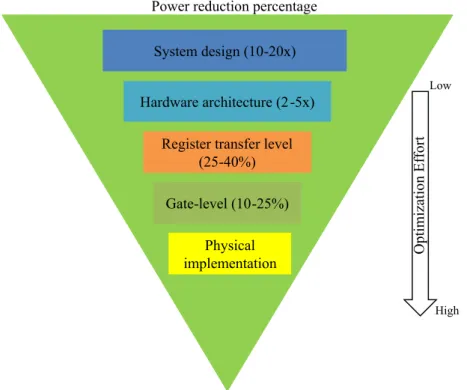
1.1 Power saving vs design effort over different levels of a design flow . 2
1.2 Power versus Technology in CMOS . . . 6
1.3 Overview of HLS based low power design methodology . . . 7
2.1 A Typical Heterogeneous System Architecture . . . 14
2.2 FPGA Architecture . . . 17
3.1 OpenCL for heterogeneous programming . . . 20
3.2 Platform and Memory Model of OpenCL . . . 20
4.1 Illustration of the KNN algorithm withk=3 andn=20 . . . 24
4.2 SDAccel Based FPGA Design Methodology Flow . . . 28
4.3 Power Estimation and Analysis Flow . . . 29
4.4 (a) Traditional global memory buffer vs (b) On-chip global memory buffer . . . 32
4.5 FPGA vs GPU execution time and energy-per-computation ratios for several test case implementations . . . 37
5.1 Flip flop with clock gating . . . 42
5.2 Header switch implementation for power gating a unit . . . 43
5.3 Complete low power design flow . . . 46
5.5 Power Up/Down Sequence . . . 50
5.6 Illustration of CG and PG integration . . . 50
5.7 JPEG decoder using IDCT module . . . 52
5.8 Power Consumption for IDCT test cases . . . 54
5.9 Area versus Power diagram for IDCT test cases . . . 55
6.1 Illustration of the CPF generation tool . . . 60
6.2 CPF generation Flow . . . 61
6.3 Complete Flow of Low Power High-level Synthesis methodology . . 63
7.1 General testbench structure for design validation . . . 66
7.2 Power Aware 32-bit Ripple Carry Adder . . . 68
7.3 Power Aware Arithmetic and Logical Unit Processor . . . 69
7.4 RCA Power curve wrt MSB_RCA workload . . . 74
7.5 ALU Power curve wrt DIV-MULT workload . . . 74
List of Tables
4.1 Target Platforms Comparison . . . 33
4.2 Performance analysis of implementation 1 . . . 35
4.3 Performance analysis of implementation 2 . . . 35
4.4 Summary of FPGA vs GPU performance results for various test cases 36 5.1 Power wrt area performance for IDCT test cases . . . 53
5.2 Toggle rates for JPEG usage . . . 53
7.1 Power versus Area for RCA . . . 73
7.2 Power versus Area for ALU processor . . . 73
7.3 Power versus Area for IDCT . . . 75 7.4 Complete IDCT design versus RAM wrt area and power consumption 75
Nomenclature
Acronyms / Abbreviations ALU Arithmetic and Logic Unit
ASIC Application Specific Integrated Circuit
BRAM Block RAM
CG Clock Gating
CGIC Clock-Gated Integrated Cells
CMOS Complimentary Metal Oxide Semiconductor
CPF Common Power Format
CPU Central Processing Unit
CU DA Compute Unified Device Architecture
DRAM Dynamic RAM
DSE Design Space Exploration
DV FS Dynamic Voltage Frequency Scaling
FIFO First-In First-Out
FPGA Field Programmable Gate Array
GPU Graphics Processing Unit
HLS High-Level Synthesis
HPC High Performance Computing
IDCT Inverse Discrete Cosine Transform
KNN K-Nearest Neighbor
MSV Multi-Supply Voltage
OpenCL Open Computing Language
PMB Power Management Block
PSO Power Shut-Off
QoR Quality of Results
RAM Random Access Memory
RCA Ripple-Carry Adder
RT L Register Transfer Level
SoC System On Chip
TCF Toggle Count Format
Chapter 1
Introduction
Modern electronic devices, driven by exceeding market requirements, are required to perform a variety of tasks. Considering the example of mobile handsets; they were initially meant to mainly support voice calls and text messaging i.e. short messaging service (SMS). Modern smart phones, in comparison, are required to support a variety of sophisticated features such as video calls, voice over IP (VoIP) and multimedia messaging to name a few. The support for such increasing features in modern electronic devices is provided by advanced system-on-chip (SoC) designs consisting of heterogeneous system architectures.
Such heterogeneous systems essentially consist of a combination of multi-core processors and hardware accelerators for speeding up the execution of compute in-tensive operations while consuming considerably lower power [1], [2]. Traditionally, graphics processing units (GPUs) have been used as accelerators in combination with central processing units (CPUs) but unfortunately high performance computing (HPC) systems based on GPUs are inefficient in terms of their power consumption [3]. Modern field programmable gate arrays (FPGAs) fortunately have the ability to offer considerable execution speed while consuming only a fraction of the power as compared to several high-end GPUs [4]. These FPGAs, hence are strong competitors to the traditional GPU-based accelerators and are part of heterogeneous systems in modern HPC systems.
It can be concluded from the discussion above that power consumption in modern SoCs is as critical as their computational abilities. Hardware designers are always looking to develop designs which are optimal both in terms of power and timing
Low
High
Fig. 1.1 Power saving vs design effort over different levels of a design flow
which unfortunately are conflicting performance parameters. It is easier to achieve pareto-optimality, if the power is considered at a higher level of abstraction i.e. at the system-level of the design flow. This is because major architectural decisions related to cost, performance and power consumption are made at higher abstraction level [5]. The opportunity to save power decreases as we go down the design flow from system-level to the register transfer level (RTL) and below, while the optimization effort increases. This is depicted in Fig. 1.1.
1.1
FPGA based heterogeneous computing system
Modern HPC systems are meant to analyze diverse range of complex phenomena in a variety of fields such as data mining, fault simulation and fluid dynamics to name a few. This requires the modern computers to provide huge computational abilities in a sustainable manner. There has been a general consensus since long that constant performance improvements in modern computers can not be obtained merely by increasing their operating parameters e.g. the processor clock speed. While such
1.1 FPGA based heterogeneous computing system 3
measures may yield performance enhancement, they also result in a higher power consumption than is desirable for modern HPC systems [6].
One of the solutions to this issue is to deploy systems that utilize accelerators e.g. GPUs and FPGAs, in combination with multi-core processors to speed up the execution of compute-intensive operations while still consuming considerably less energy. Additionally, it is desirable to expose parallelism in applications e.g. by using various parallel programming languages, so as to better exploit the parallel architectures offered by these accelerators. Such systems offer sufficient execution speed along with providing better energy efficiency [2].
GPUs are known to provide huge computational power and hence have been used extensively for HPC applications. However, with their continuously increasing computational capabilities, GPUs are also known to be extremely inefficient as far as their energy consumption is concerned [7]. The energy consumption can be significantly reduced while still having a considerable amount of computational power by utilizing FPGA-based accelerators. FPGAs are well known for their reconfigurability as well as their energy efficiency. This fact has been recognized in the industry as evident from the decisions by Microsoft and Baidu to use FPGAs as accelerators rather than GPUs in their respective search engines [8],[9].
A major limitation while utilizing FPGAs in modern heterogeneous systems is the complexity in programming them. Traditional FPGA programming requires sufficient expertise in one of the several hardware description languages (HDL) e.g. Verilog and VHDL. Hardware designers normally use these languages for FPGA programming but several useful algorithms are usually written in non hardware-specific languages e.g. C/C++. It requires a lot of effort on the part of hardware designers to port the algorithms for implementing them on FPGAs [10]. Furthermore, describing hardware at such low-level languages limits the designers to explore only a limited number of architectural options due to their much slower design and verification cycles [11].
These issues can be rectified by an approach called High-level Synthesis (HLS) which enables the designers to implement their algorithms, written in several higher level languages such as C, C++ and SystemC, directly on FPGAs. HLS causes a significant reduction in both the design and verification time and effort as compared to an HDL design. Additionally, it allows designers to have several considerably different hardware implementations, satisfying a variety of design constraints, from
a single high-level code by merely providing different directives to the HLS tool, a process called design space exploration (DSE) [12], [13].
Recognizing the abilities of FPGAs as competitors to the traditional GPU-based accelerators and the programming complexity affiliated with them, various HLS tools have been developed recently by the leading FPGA manufacturers e.g. Xilinx and Altera, for their respective devices. These HLS tools have been developed to directly support the RTL synthesis starting from the description of an algorithm in a parallel programming framework namely OpenCL developed by the Khronos group to enable execution of applications on heterogeneous platforms.
OpenCL is based upon C/C++ and is used to expose parallelism in an application to enable speed up by exploiting the concurrency offered by the hardware accelerators e.g. GPUs. It holds an advantage over the very similar Compute Unified Device Architecture (CUDA) programming framework by NVIDIA. This is due to the fact that unlike CUDA being used to program NVIDIA GPUs only, OpenCL offers higher execution portability thus enabling the execution of the same OpenCL code on a variety of hardware platforms e.g. CPUs and GPUs. With the development of HLS tools using OpenCL code as an input, the same code used to execute the application on a CPU/GPU can now be used for FPGA implementation as well with the same optimization effort as that on CPU/GPU-based platforms [14].
As mentioned before, OpenCL offers execution portability but unfortunately, it does not offer performance portability. This implies that even though the same OpenCL code can be executed on a variety of hardware platforms, the performance would vary from one device to another. OpenCL implementation and optimization support on Xilinx FPGAs is provided by the SDAccelTM tool chain from Xilinx, utilizing tools from Vivado®design suite for RTL and logic synthesis [15], [16].
1.2
High-level synthesis based low power
methodol-ogy
Fig. 1.1 shows that maximum power can be saved by specifying power intent at the system-level of the hardware design flow. This would also require the least optimization effort as compared to the cases where optimization is considered at lower levels of abstraction. In a conventional design flow, the designers must
1.2 High-level synthesis based low power methodology 5
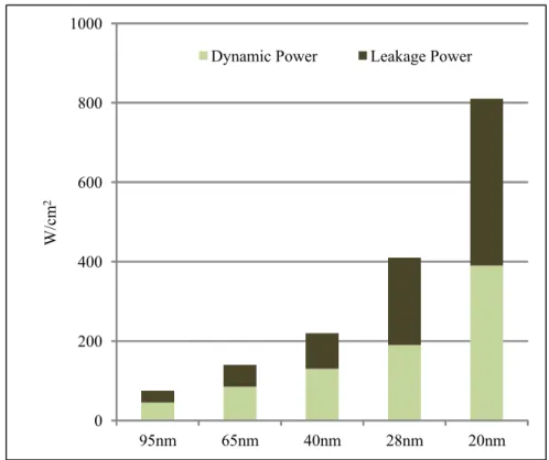
optimize manually written RTL to satisfy strict power requirements by applying numerous power optimization techniques to optimize both the leakage power as well as the dynamic power. This process involves taking into account a complex multi-dimensional problem space while considering a variety of low-level information regarding the RTL design within a strict time limitation. This obviously becomes extremely difficult and the solution is to raise the level of abstraction above the RTL for easier power optimization and to utilize RTL synthesis automation tools [17]. The power optimization techniques usually target supply voltage and clock control methodologies e.g. power shut-off (PSO), dynamic voltage frequency scaling (DVFS), clock gating (CG) and multi-supply voltage (MSV). PSO is particularly useful to reduce leakage power in hand-held devices which are usually powered by energy sources (e.g. batteries) that can only provide a limited amount of energy [18]. Previously, the total power dissipation in a complimentary metal oxide semi-conductor (CMOS) was dominated by the dynamic power but leakage power has now become an equally significant contributor with the prevailing nanometric tech-nologies. It can be assumed that this situation would continue to worsen with the continuous scaling of technology. Fig. 1.2 clearly shows this trend [19]. Dynamic power consumption in CMOS occurs during the active mode when the signals through the CMOS toggle hence changing their logic states, resulting in the charging and discharging of load capacitors [20]. Leakage power on the other hand consists
ofactive leakage andstandby leakage. The standby leakage power consumption
occurs during circuit sleep mode while the active leakage is caused by the leakage current that still flows even in the operation mode. The active leakage becomes a significant contributor to the leakage power in deeply scaled devices [21].
As discussed before, HLS takes a high-level description of a design and automati-cally generates several RTL descriptions satisfying different area/performance/power constraints thus reducing both the design and verification time and effort. It certainly is desirable to have a fully automated low power flow, enabling the incorporation of both logic as well as power into the design starting from the system-level. This would require a methodology to automatically capture the power intent of a de-sign at the system-level while using HLS to achieve a broad set of target system implementations.
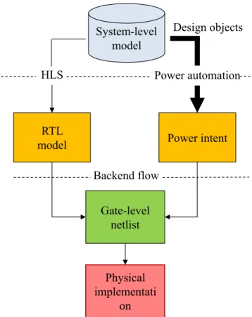
A broad overview of such a methodology is shown in Fig. 1.3. Unlike the traditional methodology involving power intent definition together with the RTL,
0 200 400 600 800 1000 95nm 65nm 40nm 28nm 20nm W/ cm 2
Dynamic Power Leakage Power
Fig. 1.2 Power versus Technology in CMOS
this methodology involves defining power intent directly using the system-level code and using HLS to automatically generate the RTL. This is followed by applying the already defined power intent in the later stages of the design flow to achieve power optimization. High-level synthesis preserves the naming convention of the design hierarchy including instances, signals and ports. This in turn enables designers to directly define power intent on the system-level code, which is more convenient to understand owing to its higher level of abstraction. Additionally, adding power management logic at the system-level makes functional verification simpler via the design-specific system-level testbench [5].
1.3
Problem Statement
This dissertation deals with some issues regarding high-level synthesis in general and low-power hardware accelerator design in particular. FPGAs can be categorized as reconfigurable digital hardware which have been used in a variety of applications ranging from signal processing to high performance switches. They also represent
1.3 Problem Statement 7 Power intent RTL model Gate-level netlist Physical implementati on HLS Design objects System-level model Power automation Backend flow
excellent options as accelerators due to their flexibility, energy efficiency and high performance. FPGAs are usually programmed using hardware description languages like verilog or VHDL. To be proficient in these languages, one needs to have considerable knowledge about computer architecture and hardware design [10]. This programming complexity affiliated with FPGAs has been the reason for reluctance shown by designers in using FPGAs as accelerators. HLS, however, gives us a way around this issue by allowing us to program the FPGAs directly through C/C++ and other programming frameworks based on them e.g. SystemC and OpenCL. With this issue being taken care of, FPGAs can be strong competitors to the prevailing trend of using GPUs as hardware accelerators.
With regards to obtaining energy-efficient application specific integrated circuit (ASIC) designs, describing power intent at the system-level is still a stiff challenge for system architects and designers. Power optimization is usually considered at the RTL in a conventional design flow when most of the architectural decisions have already been made. It is thus desired to have a methodology that enables the description of both the behavioral functionality as well as the power intent at a higher level of abstraction while using HLS tools at the front end of the proceeding design flow. There, however, exists no commercial tools or methodology presently for this purpose and the required effort must still be done manually. A brief overview of the methodology which can yield this automation has been shown in Fig. 1.3.
1.4
Contribution
One of the goals of the thesis is to explore a methodology using HLS to imple-ment an application written in OpenCL on an FPGA-based accelerator. The main contributions from this activity are:
• investigation of the issues encountered when implementing and optimizing a code, written in non-hardware specific OpenCL on a Xilinx FPGA device. The methodology is based on HLS and it is intended to apply a variety of HLS optimization attributes and techniques and see how an OpenCL code responds to them to yield the desired performance on an FPGA.
• secondly, it is also intended to emphasize on the difference in compilation of an OpenCL code to be executed on a GPU and an FPGA, stemming mainly
1.4 Contribution 9
due to their different architectures. While GPUs due to their fixed architecture, support just-in-time compilation, the FPGAs due to their flexible architec-ture, allow a more thorough exploration of various code optimizations than allowed by just-in-time compilation. The OpenCL standard thus, allows offline compilation of the OpenCL code to be executed on an FPGA.
• finally, it is shown by comparing the performance of multiple algorithm im-plementations on various platforms that the code executing efficiently on an FPGA is very different from the one leading to the best implementation on a GPU.
The thesis also deals with the development of a methodology based on HLS to automatically generate power optimization directives to achieve PSO (leading to reduced leakage power) in an ASIC design in the form of a common power format (CPF) file by using the relevant information, extracted from the system-level design e.g. the module to be shut-off, as well as other important information e.g. technology specifications. CPF is a standard endorsed by the low power coalition at Silicon Integration Initiative (Si2) and can be used to describe power intent for a design [22].
It should be noted that large FPGAs (with several transistors) also suffer from huge leakage power consumption. This is because of the increase in leakage compo-nent of each of the several transistors embedded into modern heavily scaled FPGAs. Furthermore, in large FPGAs, a sizeable portion of the available resources may remain unutilized if the design does not fill up the device completely. This would result in leakage power due to both the utilized and unutilized parts of the FPGA [23].
The authors in [24] have proposed a method to reduce the leakage power sig-nificantly in FPGAs by shutting down individual accelerators dynamically during idle periods at run-time through a technique called dynamic power-gating. The same authors in [25] also present a technique to achieve fine-grained power gating by shutting down selected portions of hierarchical designs with large accelerators i.e. sub-accelerators, while the rest of the sub-accelerators are still running. The identification of idle states along with their duration however, in FPGAs is very difficult to achieve thus discouraging designers to make the required effort. Power gating in ASIC designs however is much more common, wherein, the opportunities for power gating can be identified manually and exploited using standard file formats
such as unified power format (UPF) or CPF [23]. Hence, it is worthwhile to note that while many of the optimizations used during the course of the first activity are relevant both for ASIC and FPGA designs, the second activity (concerned with using CPF for power gating) pertains exclusively to an ASIC design. The main contributions from this activity are:
• exploring issues encountered while obtaining a fully automated low power ASIC design flow starting from the system-level description to the physi-cal design. This would involve the development of a generic system-level power management module to enable firstly the specification and later on the application of the power intent to achieve a power efficient design.
• development of a tool that can automatically generate the power optimization directives to achieve PSO for a given system design context.
1.5
Organization of the thesis
This thesis presents a collection of the work done in the field of electronic design automation using high-level synthesis with an emphasis on power/energy efficient designs. The first activity deals with an exploration of the prospects of using FPGAs as accelerators in modern heterogeneous systems by utilizing HLS along with their performance comparison with some high-end GPUs. This activity is covered in this document from chapters 2 to 4. The second activity explores the idea of developing a fully automated low power design methodology complementing the HLS to obtain power-efficient ASIC designs. The details can be found in chapters 5, 6 and 7. Chapter 8 concludes the work along with mentioning some future directions in which both the activities can be pursued. A brief description of each chapter is presented here.
Chapter 2: Basic theory regarding heterogeneous system architectures is pre-sented here with reference to both GPU- and FPGA-based acceleration.
Chapter 3: This chapter gives a description of OpenCL programming language which is a parallel programming framework and enables execution portability over a variety of device platforms.
1.5 Organization of the thesis 11
Chapter 4: This chapter compares FPGAs versus GPUs in terms of execution speed, power and energy consumption. This is done by utilizing a widely used classification algorithm i.e. K-Nearest Neighbor (KNN), as a test case.
Chapter 5: This chapter explains the details regarding system-level power management module which enables the provision of signals necessary to achieve power gating thus yielding a power-efficient ASIC design.
Chapter 6: The description of our proposed low power HLS-based methodology (LP-HLS) is presented here along with a description of the tool that we developed to automatically derive the power optimization directives necessary to achieve PSO.
Chapter 7: This chapter presents the design test cases that were used to validate our LP-HLS methodology. The results validating our proposed methodology are also presented.
Chapter 8: The work is finally concluded along with a brief description of the future directions in which the activities can be pursued.
A sample CPF file used for power gating one of our test cases i.e. an Inverse Discrete Cosine Transform (IDCT) design in a JPEG IDCT decoder is provided in Appendix A.
Chapter 2
Heterogeneous System Architecture
A heterogeneous system refers to a system comprising of several different processors and cores. Such multi-core architectures offer high performance along with better power efficiency by not only using additional processor cores but by using specialized hardware calledacceleratorsto handle certain computationally challenging portions of the applications.
2.1
Why Heterogeneous architecture?
Besides the complexity i.e. the number of transistors per square inch of a processor, the processor frequency also traditionally follows the Moore’s low very closely. This trend of a continuous increase in the frequency has however been hindered by certain physical constraints e.g. the power density [26]. The equation for power density specifically depicting the influence of frequency is given by (2.1):
P=Cρf Vdd2 (2.1)
wherePis the power density i.e. the power dissipated per unit area,Crepresents the total capacitance,ρ is the transistor density i.e. the number of transistors per unit
area, f represents the processor frequency andVdd is the supply voltage [27].
It should be noted that (2.1) ignores the leakage power which contributes signifi-cantly to the over all power consumption in CMOS sub-micron technologies [28].
Kernel Compute Unit Compute Unit Compute Unit PE PE PE PE GPU FPGA Kernel Infrastructure IP Memories Kernel PCI express Processor Host Memories
Fig. 2.1 A Typical Heterogeneous System Architecture
As evident from (2.1), the clock frequency of the processor can not be increased unbounded due to the so calledpower wall.
One of the solutions to improve performance while still keeping the power consumption in check, is to use multi-core processors running at lower frequencies and supply voltages than the single core processors. For example, a dual core design running at 85% of the supply voltage and frequency offers 180% better performance while still consuming approximately the same power as a single core design [26]. The issue with the multi-core processors in use presently though, is that most of their resources are spent on logic and cache thus, resulting in majority of the power being consumed by non-computational units.
Heterogeneous architectures give us an alternative solution to this issue. These architectures utilize the multi-core processors in combination with high performance accelerators for a given power or transistor budget. This essentially means that the accelerators use fewer transistors and operate at lower frequencies as compared to the CPUs hence consuming lower power/energy. These accelerators typically do not operate standalone and rely on traditional processors to manage them. This implies that the CPUs are responsible to explicitly manage data transfer and execution while using the accelerator cores [26], [29]. The accelerators used in such heterogeneous systems may be GPUs, FPGAs or a combination of both. In the terminology of heterogeneous system architecture, the multi-core processor is typically called ahost
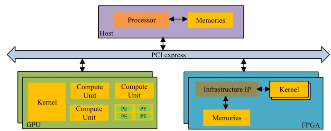
while the hardware platforms used to accelerate certain portions of the applications are calleddevices. A typical heterogeneous system is shown in Fig. 2.1. The various important components of such a heterogeneous system are described here briefly.
2.2 Multi-core processors 15
2.2
Multi-core processors
As mentioned earlier, increasing clock frequency to achieve better processor per-formance is not a viable option due to the corresponding significant increase in energy, heat dissipation e.t.c as represented by (2.1). One way of countering this is to lower the clock frequency while packing more processor cores in a chip i.e. the
multi-core processors. These multiple cores will share some resources e.g. memory, network etc but are still capable of handling independent operations. Such processors enable the developers to exploit both data-level and task-level parallelism. To fully exploit the capabilities of such multi-core processors, the programmers may need to write multi-threaded codes, utilize libraries offering shared memory parallelism e.g. OpenMP or use a message passing library e.g. MPI [10].
2.3
Graphics Processing Units
Another option to speed up the execution of parallelizable portions of the algorithms is to use GPU-based accelerators as co-processors. A GPU is in principle a device consisting of an extremely parallel microprocessor and a private memory with a very high access bandwidth. They were originally developed to cater to the increasing demand for hardware accelerated 3D graphics. The interest in the use of GPUs for HPC applications started developing with the introduction of CUDA parallel programming framework by NVIDIA in 2007. GPUs are meant to execute in parallel, the same set of instructions on different data in single instruction multiple data (SIMD) fashion. Unlike multi-core CPUs, the GPUs are designed in such a way so as to devote more transistors to data operations instead of data caching and control [26].
A GPU consists of several parallel processing elements called streaming multi-processors to execute the kernel functionality in a parallel manner. Each streaming multiprocessor further consists of multiple cores, with each core made up of sev-eral components such as arithmetic and logical units (ALUs), thread-schedulers, load/store units, scratchpad memories, caches etc. The cache size in GPUs is much smaller as compared to the CPUs as they are designed for stream or throughput computing involving smaller data reuse as compared to the CPUs. A GPU always acts as a device in combination with a CPU being used as a host for loading data
intensive tasks on the GPU and offloading the results along with managing the data transfers involved in the process. A GPU consists of its own device memory of a few gigabytes (GBs) and is connected to the host through a PCI-Express (PCIe) bus as shown in Fig. 2.1 [7].
2.4
Field Programmable Gate Arrays
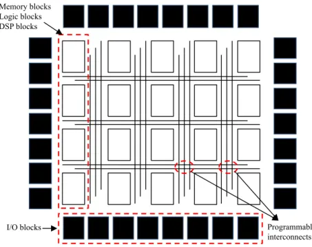
While GPUs offer great computational abilities that can be exploited while using them as accelerators, they unfortunately have a very poor power efficiency [7], [3]. FPGAs provide an alternate option as accelerators offering considerable computa-tional abilities while still consuming considerably small amount of power/energy as compared to the several modern high end GPUs. This is mainly because of the control systems in FPGAs being hardwired hence, eliminating the need to fetch, decode and execute instructions. Furthermore, the on-chip SRAM in case of FPGAs are better customizable to the specific applications, thereby cutting on the multi-plexing energy costs. While FPGAs were initially used for discrete logic, there has been a drastic expansion in their fields of usage ranging from signal processing to high performance embedded computing and more recently in high performance computing [26]
FPGAs offer a highly parallel architecture which can be used to achieve a considerable amount of acceleration. A typical FPGA consists of logic blocks, memory blocks and DSP slices each surrounded by programmable interconnects as shown in Fig. 2.2. The FPGAs offer high performance along with high versatility and power efficiency owing to their conceptually simpler design [26]. The idea of using FPGAs as accelerators normally suffers due to the complexity involved in programming them. This issue however, can be resolved by using e.g. SDAccelTM tool chain from Xilinx which enables us to program Xilinx FPGAs directly using the OpenCL parallel programming language. The tool chain includes both the Vivado high-level synthesis tool as well as the logic and physical design tools from the Vivado®design suite [15], [16].
2.4 Field Programmable Gate Arrays 17
Memory blocks Logic blocks DSP blocks
I/O blocks Programmable
interconnects
Chapter 3
Open Computing Language
OpenCL is a parallel programming framework for programming multi-core and heterogeneous compute platforms [30], [31]. Thus, it lies at the intersection of the programming languages corresponding to the individual computing platforms constituting a heterogeneous system as shown in Fig. 3.1. OpenCL offers execution portability thus enabling code execution on various supporting devices through minimal modifications to the host code. The programming language is based on C99 and supports both data-parallel and task-parallel programming models [26].
3.1
Platform Model
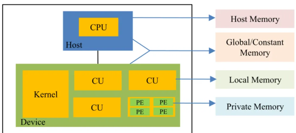
The OpenCL platform model mainly consists of a multi-core CPU called a host. Host is responsible for setting up the environment to enable an OpenCL program to execute on one or more devices. In terms of OpenCL, adevice represents any supported hardware platform that can be used to accelerate the compute intensive portions of an application referred to as thekernels. An OpenCL device consists of compute units (CU) each further divided into processing elements (PE) as shown in Fig. 3.2. Several concurrent executions of the kernel body (calledwork-items) takes place on multiple processing elements. The work-items are further grouped intowork-groupswhich are being executed by multiple compute units.
CPU Multi-cores giving performance increase GPU Data-parallel computing Multi-processor programming Graphics APIs OpenCL Heterogeneous Computing Emerging Intersection
Fig. 3.1 OpenCL for heterogeneous programming
CPU Host Kernel CU CU CU PE PE PE PE Device Host Memory Global/Constant Memory Local Memory Private Memory
Fig. 3.2 Platform and Memory Model of OpenCL
3.2
Memory Model
The memory is broadly divided into host (i.e. CPU) memory and device (i.e. GPU or FPGA) memory. The device memory is further divided into private memory (specific to each work-item). This memory is the smallest i.e. O(10) words per work-item but is the fastest to access at the same time. Local memory is shared by all the work-items in a work-group and is around O(1-10) kbytes per work-group. This is also slower than the private memory. Global/constant memory is shared by all the work-groups. Global memory is around O(1-10) Gbytes while constant memory is around O(10-100) Kbytes. Access to the global memory is the slowest among all the device memories. Finally, the host memory resides on the CPU and can be few Gbytes in size. The OpenCL memory model is also shown in Fig. 3.2. It should be noted that memory management in OpenCL is done explicitly i.e. by moving data from host memory to global memory to local memory and then back.
3.3 Synchronization in OpenCL 21
3.3
Synchronization in OpenCL
The work-items in an OpenCL kernel are executed in an out-of order manner to ensure high performance by relieving the programmer i.e. by extracting parallelism from the code automatically and speeding it up on a given hardware platform [32]. Since the execution order of work-items across different devices can not be ascertained, OpenCL standard introduces the concept ofbarriersto ensure memory consistency. A barrier represents a check point with in a group such that all the work-items belonging to that work-group must reach this point before any of them can proceed with the rest of the computations [15]. Synchronization in the execution of work-items belonging to different work-groups is not possible in OpenCL.
Chapter 4
Battle of Accelerators: FPGA or
GPU?
This chapter describes the adopted HLS-based methodology to implement a popular classification algorithm i.e. the K-Nearest Neighbor algorithm, on Xilinx FPGAs. Multiple implementations of the algorithm are considered and their performance on FPGA and GPUs is compared as well.
4.1
KNN Algorithm
K-Nearest Neighbor (KNN) algorithm is an important algorithm for classification finding applications in a diverse range of fields such as computer vision, pattern recognition and machine learning etc. KNN can be used to detect the k nearest neighbors of a specific query point among severel reference data points. Usually, the training datasets are very large, thus causing the computation cost of the algorithm to be very large [33]. Fortunately, the algorithm consists of a high level of parallelism and hence, we can accelerate it considerably by utilizing the parallel architectures of GPUs or FPGAs. The algorithm consists of the following steps:
1. For givennnumber of points in the reference data setRand a specified query pointq, find thendistances between the query point and each point in the reference data set. Squared Euclidean distance is used here i.e. for two
bi-Fig. 4.1 Illustration of the KNN algorithm withk=3 andn=20
dimensional points (x1,y1) and (x2,y2), the Squared Euclidean distance is given by (4.1).
d= (x1−x2)2+ (y1−y2)2 (4.1)
2. Sort thendistances calculated in step 1 while maintaining the corresponding indices of the points in the reference data setR.
3. Return thekpoints in the reference data setRrelative to theksmallest distances obtained from step 2.
For a setR ofn reference (training) data points in a d-dimensional space and a query pointq, the k-nearest neighbor algorithm returns thekpoints inRthat are closest to the query pointq. This is illustrated fork = 3andn = 20in Fig.4.1. The red sphere represents the query point while the blue diamonds represent the points of the reference data set.
4.2
Related Work
The use of FPGAs as an alternative option to the traditional GPUs for acceleration has already been highlighted before. Some relevant work in this domain is presented here. In addition, this section of the thesis also mentions some work done previously to accelerate the KNN algorithm.
A thorough performance comparison between a CPU, a GPU and an FPGA implementation of a complex computer vision algorithm targeting linear structure detection has been presented in [34]. The authors in that work demonstrated that
4.2 Related Work 25
the FPGA used i.e. the Xilinx Spartan LX150 FPGA outperformed both the AMD Radeon HD6870 GPU and the Intel Core i7 processor in terms of both the power consumption and the execution speed. OpenCL was used in that activity to port the code from CPU to GPU while VHDL was used for the implementation on their FPGA counterpart. The manual effort for this translation was also studied. This effort was certainly found to be higher for the VHDL-based FPGA implementation than for the OpenCL-based GPU implementation. We however, used an HLS-based approach for FPGA implementation starting directly from the OpenCL-based GPU implementation. This certainly causes a considerable reduction in the overall design effort along with giving us the ability to generate multiple hardware implementations from a single high-level OpenCL code merely by providing different directives to the HLS tool.
The authors in [10] have performed a very detailed performance comparison of multiple hardware accelerators for several implementations of the quantum Monte Carlo application. Numerous programming languages i.e. CUDA, OpenCL, C++, Brook+ and VHDL, have been used for various hardware platforms such as Intel multi-core CPUs, several GPUs from Radeon and NVIDIA and a Xilinx Virtex 4 LX160 FPGA. The analysis carried out in that paper for a large number of computa-tions resulted in the combination of CUDA and NVIDIA GPUs providing the best performance while the FPGA performed the worst. The authors identified the main reason for this, as using older FPGA against extremely powerful GPUs and CPUs. The authors in that work also described their experience regarding the complexity of programming FPGAs through VHDL which took them about an year to perform.
An FPGA-based heterogeneous platform for KNN implementation was presented in [35]. Compilation of the OpenCL code onto the FPGA was carried out by using Altera’s OpenCL compiler. A variety of hardware platforms were considered e.g. an Intel Core i7-3770 processor, an AMD Radeon HD7950 GPU and a Stratix IV 4SGX530 FPGA from Altera. The authors in that paper managed to obtain an FPGA implementation that outperformed both the GPU and CPU in terms of power/energy consumption per computation. The GPU implementation however was found to be faster than the FPGA implementation, most probably due to the GPU’s higher global memory access bandwidth.
Various parallelization techniques corresponding to the nearest neighbor algo-rithm were surveyed in [36]. The author strongly emphasized both the requirement as
well as the opportunity to parallelize such algorithms. Acceleration of a brute force nearest neighbor algorithm through GPUs (while utilizing CUDA and CUBLAS library) was proposed in [33],[37]. Obviously, a huge increase in execution speed as compared to a highly optimized C++ library was obtained as a result.
It can thus be concluded that FPGA can be a favorable option in comparison to GPU for acceleration especially, when energy-per-computation is the main deciding factor. The designers in Baidu are thus weighing their options to use FPGAs as accelerators for their deep learning models for image search [8]. Microsoft also recently announced their decision of using FPGAs as accelerators in combination with Intel processors in their Bing search engine [38]. Considering the demand for FPGA-based acceleration in combination with their programming complexity, main FPGA manufacturers i.e. Altera and Xilinx, have also recently developed HLS tools enabling designers to implement the OpenCL codes directly on their respective FPGAs [15], [39]. This is hence, a hot topic for the design community at present and hence this motivated us to carry out an extensive research work in this regard.
4.3
Methodology
This section describes our adopted methodology to implement the algorithm on an FPGA starting from its OpenCL code. The power analysis flow is presented as well.
4.3.1
FPGA Implementation
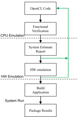
Fig. 4.2 depicts the various steps performed by the SDAccel tool from Xilinx for direct FPGA implementation of an input OpenCL code. The flow begins with the functional verification of the OpenCL code through a software (SW) based simulation called CPU emulation in the context of an SDAccel-based flow. CPU emulation represents the fastest step of this design flow enabling a quick verification of the design functionality. An x86-based CPU is used in this step to execute both the host and kernel codes [15].
This step normally consists of adding a testbench to the host code, which performs the same functions in software as done in hardware and then compares the results from both. The testbench setup generates stimuli to drive the data and control ports of
4.3 Methodology 27
the design under test (DUT). Furthermore, it monitors the output thereby validating the functionality of the DUT. Once the functionality is verified, the performance of each individual kernel i.e. the performance of an individual compute unit (in case of OpenCL, it is a work-group) and its resource usage are estimated. This gives an early estimate of the eventual performance gains by considering the targeted hardware platform along with the generated compute units for executing the application.
This is followed by RTL simulation using the same testbench that was used for CPU emulation. This step in the SDAccel-based flow is called hardware (HW) emulation and is used for functional verification of the compute units which are created for all the kernels and for their overall performance analysis. While CPU emulation ensures the functional accuracy of the application, its functionality on the hardware is verified by HW emulation. SDAccel needs to generate the logic implementation for each compute unit before HW emulation. This step hence, takes longer to complete in comparison with the CPU emulation. Vivado HLS is run under the hood in this step for custom logic generation corresponding to the application hence maximizing performance and minimizing resource utilization at the same time. VivadoTMIntegrated Design Environment (IDE) is utilized afterwards in thebuild applicationstep for connecting the generated custom units to the infrastructure IPs provided by the target hardware, such as the interface for the processor which is used to pass arguments to the kernel to start its execution and wait for its completion and the DDR DRAM interface [15]. Finally the generated system is packaged to be deployed on the supported FPGA-based boards.
4.3.2
Power Analysis
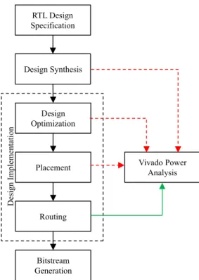
The power consumption in case of the FPGA implementation is estimated by utilizing the power analysis capabilities of Vivado®. Vivado supports power estimation through all the steps encompassing the FPGA design beginning with the logic synthesis up to the "place and route" stage. We perform power estimation in this work after the design is routed. This is because, the power analysis at this stage is the most accurate as it is based on the exact logic and routing resources being read from the already implemented design database [40]. The complete power analysis flow based on the Vivado power analysis features is shown in Fig. 4.3.
OpenCL Code Package Results HW emulation Build Application System Estimate Report Functional Verification CPU Emulation HW Emulation System Run
Fig. 4.2 SDAccel Based FPGA Design Methodology Flow
The power analysis can either be performed by using the default switching probabilities assigned to the design primary inputs by Vivado. The tool propagates these values to all the internal signals as well. This method is not as accurate as the vector-based power estimation. The vector-based estimation consists of RTL simulation and extraction of switching information of the design by performing activity profiling using test vectors provided to the design input ports as stimuli. The vector-based estimation is more accurate but the process takes considerably longer time to complete. In comparison, power estimation, based on default switching probabilities, provides a good trade-off between the accuracy in power estimation and the compute efficiency [40].
We used the vector-based approach to estimate power more accurately in the case of FPGA implementation. Switching Activity Interchange format (SAIF) file was used to capture the switching activities for the design which were then utilized to obtain accurate power reports. The GPU power on the other hand was estimated by using the NVIDIA system interface utility (nvidia-smi) that exploits the NVIDIA Management Library (NVML) and can be used to profile and manage all the NVIDIA GPUs installed on a specific platform [41].
4.4 Test case implementations 29 RTL Design Specification Bitstream Generation Placement Routing Design Optimization Design Synthesis Design Implementation Vivado Power Analysis
Fig. 4.3 Power Estimation and Analysis Flow
4.4
Test case implementations
The baseline code in this activity is based on the parallel implementations from [42], [43]. Two significantly different versions of the KNN algorithm are considered and their GPU- and FPGA-based implementations compared in terms of execution speed, energy and power performances. The implementations differ mainly based on whether the neighbor estimation is performed on the processor or on the accel-erator. In case where the CPU estimates the neighbors, the CPU execution time is also considered while calculating the execution time of the algorithm. The two implementations are presented here.
4.4.1
Implementation 1
This implementation uses a parallel execution of the distance calculation task of the KNN algorithm on the device (GPU/FPGA), while the nearest neighbor estimation is performed on the host. The distance calculation task is readily parallelizable, as distinct independent points are read from the reference data set for calculating
several distances. The implementation utilizes global memory accesses only and hence its performance mainly depends on the global memory access bandwidth of the various accelerators. It is illustrated in Implementation 1.
Implementation 1:Distance calculation on device and neighbors on host
Input: A query pointqandR, a set of reference points;
Output:Indices of thekreference points with the smallest distance fromq;
1 Begin
2 On device:
3 functionDISTANCE CALCULATION
4 foreach reference point r∈Rdo
5 compute the floating-point distances betweenqand all pointsr∈R; 6 end
7 end function 8 On host:
9 functionNEIGHBOR ESTIMATION
10 fori = 0 to k−1do
11 print the index inRof thei−thsmallest element of the sorted distance
vector;
12 end
13 end function 14 End
4.4.2
Implementation 2
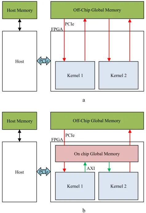
This implementation performs both the distance calculation as well as the neighbor estimation task on the device in two separate kernels namely "DISTANCE CALCU-LATION" and "NEIGHBOR ESTIMATION" respectively. It utilizes an automatic optimization offered by SDAccel called "On-chip global memories". This option automatically maps the global memory buffers used merely for inter-kernel com-munication, to the on-chip block RAMs. This optimization is depicted in Fig. 4.4. It should be noted that the global memory buffers are normally mapped to exter-nal slower DRAMs. This is shown in Fig. 4.4 as well. The pseudocode for this implementation is given in Implementation 2.
This implementation makes sense with reference to acceleration of the KNN algorithm only for the dimensionality of each point ofRbeing high, thus making
4.5 Experimental Setup 31
the distance computation task more dominant as compared to finding theksmallest distances.
Implementation 2:KNN on device using multiple kernels
Input: A query pointqandR, a set of reference points;
Output:ksmallest floating-point distances with their indices in a single work-group;
1 Begin
2 On device:
3 declare a floating-point global distance array "dist" for inter-kernel
communication;
4 functionKERNEL1: DISTANCE CALCULATION
5 foreach reference point r∈Rdo
6 compute all the floating-point distances betweenqand all pointsr∈Rand
save in "dist";
7 end
8 end function
9 functionKERNEL2: NEIGHBOR ESTIMATION
10 fori = 0 to k−1do
11 print the index inRof thei−thsmallest element of the distance vector; 12 end
13 end function 14 End
4.5
Experimental Setup
The experimental setup consists of three target devices shown in Table. 4.1. The first device is an NVIDIA GeForce GTX960 GPU with 1024 cores and a maximum operating frequency of 1178MHz. The device has about 2GB GDDR5 of global memory, with 112GB/s of memory bandwidth. It is accessible from the host through a PCIe 3.0 interface with 16 lanes. The second device is an NVIDIA Quadro K4200 GPU with 1344 CUDA cores and a maximum clock frequency of 784MHz. The device has about 4GB of GDDR5 global memory, with 172.8GB/s of memory bandwidth. It is accessible from the host through a PCIe Gen2 interface with 16 lanes. The third device is an Alpha data ADM-PCIE-7V3 FPGA board with a Virtex-7 690t. The global memory consists of two DDR3 memories with 21.3GB/s of bandwidth. The host can access it through a PCIe Gen3 interface with 8 lanes.
Off-Chip Global Memory Host Memory
Kernel 1 Kernel 2
Host PCIe
FPGA
Off-Chip Global Memory Host Memory
On chip Global Memory
Kernel 1 Kernel 2 Host PCIe FPGA AXI PCIe a b PCIe
4.6 Results 33 Table 4.1 Target Platforms Comparison
Device Global Memory Size Bandwidth (GB/s) Bus In-terface min tclk Datasheet Power (W) Idle Power (W) GTX960 2GB GDDR5 112.0 PCIe 3.0 x16 0.85ns 120 8 K4200 4GB GDDR5 172.8 PCIe 2.0 x16 1.27ns 108 13 FPGA Two 8GB SODIMMs 21.3 PCIe 3.0 x8 * -
-* See the rest of the tables for the reported clock and the actual power values in each test case.
4.6
Results
The experiments with the KNN algorithm use the data set from [44]. It contains data from "Unisys corporation" consisting of locations (latitudes and longitudes) of a number of hurricanes and is used by the KNN algorithm to find the locations corresponding to k nearest hurricanes to a given query point. The value ofk is typically very small as compared to the number of pointsnin the reference data set.
khas been set to 5 in all our experiments. The number of points in the reference data set is about 0.3 million.
In case of the FPGA implementation, the concurrency offered by the FPGA is utilized by using several HLS-based optimizations offered by SDAccel. The (reqd_work_group_size) attribute described by the OpenCL standard has been used in both implementations to specify the number of work-items in a single work-group. This in turn specifies the iteration count of the work-item loop which enables the HLS tool to optimize performance while the custom logic for the kernel is being generated. 2-element vector data types were used in both cases (rather than the C structs) to read the 2-dimensional data points, thereby causing the memory access throughput to be improved. Another optimization which was used in both the implementations is the use of burst transfers between the the off-chip global memory and the on-chip local memory. Large bursts improve efficiency as the memory access overhead is shared across large amounts of data being transferred [14].
Moreover, loop pipelining was used as well to improve throughput. The SDAccel-based flow can pipeline both the work-item loops as well as any explicit loops in the
kernel. Pipelining overcomes the limitations of loop unrolling for loops accessing global memory as in our case, by better matching the limited number of global memory ports available. The limited number of global memory ports may result in data access conflicts thereby limiting the performance gains obtained by loop unrolling by serializing potentially parallel loop iterations [45].
The GPU versus FPGA results in terms of execution time, energy and power consumption for Implementation 1 are presented in Table 4.2. The resource uti-lization in case of FPGA is also given in the table. This implementation utilizes the accelerators merely for distance calculation between the query point and all the points of reference data set. The nearest neighbor estimation on the other hand is performed by the host i.e. processor, hence the CPU time is added as well to the table as a part of the total KNN execution time. The reported clock frequency by Vivado HLS in this case is 240MHz.
As clear from Table 4.2, both GPUs in Implementation 1 are faster than the FPGA due to their comparatively higher DRAM access bandwidth. The FPGA however, consumes significantly smaller energy/power in comparison to both the GPUs. As mentioned before, power analysis in case of FPGA is done by using power analysis features of Vivado. The reported power in case of the GPUs is based on the results we obtained by utilizing the NVIDIA system management interface utility.
The performance comparison for Implementation 2 is shown in Table 4.3 This implementation is also operating at 240MHz clock frequency. This implementation uses the "on-chip global memories" optimization option offered by SDAccel to map the global memory buffers used for communication between multiple kernels to the block RAMs. A global memory buffer called "dist" as shown in Implementation 2 has been used for inter-kernel communication. This is an automatic optimization provided by SDAccel for the cases where it detects a global memory buffer which is not required to be visible to the host.
The FPGA implementation in this case is significantly faster than both the GPUs. The two kernels are executed sequentially on the GPUs and the slower DRAM is utilized. Reasons contributing to the high latency of DDR lies in the complexity. The DDR interface uses a controller to manage the refresh cycles, address multiplexing and interface timing [46]. In addition to latency, these frequent refresh cycles cause a higher power overhead as well [47]. These kernels on FPGA however, utilize the block RAMs (i.e on-chip global memories) and are executed in a pipelined manner.
4.6 Results 35 Table 4.2 Performance analysis of implementation 1
Parameters/Devices
FPGA
GTX960
K4200
Device time
1.24ms (
t
clk=
4
.
17
ns
)
0.04ms
0.05ms
CPU sort time
3.0ms
3.0ms
3.0ms
Total time
4.24ms
3.04ms
3.05ms
Power (Device)
0.346W
30W
40W
Energy (Device)
0.43mJ
1.2mJ
2mJ
Utilization
BRAMs = 0
NA
DSPs = 12 (0.33%)
FFs = 3109 (0.36%)
LUTs = 2006 (0.46%)
Table 4.3 Performance analysis of implementation 2
Parameters/Devices FPGA GTX960 K4200 Total time 1.23ms (tclk=4.17ns) 0.93s 3.11s Power 2.56W 90W 60W Energy 0.003J 84J 187J Utilization BRAMs = 512 (34.83%) NA DSPs = 12 (0.33%) FFs = 23892 (2.78%) LUTs = 11838 (2.76%)
Considering that the on-chip global memory is implemented on the FPGA itself, it has low latency and high throughput. Moreover, the NEIGHBOR ESTIMATION kernel also performs faster on FPGA than on the GPU. This is because, GPUs do not handle conditionals very efficiently, while they can still be pipelined on an FPGA. These conditionals on the GPUs create the so-called "thread divergence" problem. This issue arises due to the fact that on such Single Instruction Multiple Data processors, the work-items, for which the condition is adjudicated as false, must stall while the rest of the work-items are executed and vice-versa. The FPGA also out-performs both GPUs in terms of power and energy consumption. The FPGA power consumption in this case however, is around seven times higher than the FPGA implementation of Implementation 1. This is because of the excessive block RAM accesses that were not present in Implementation 1.
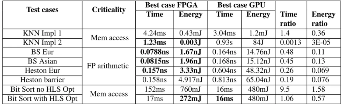
The FPGA vs GPU performance comparison for few other important algorithms, i.e. Montecarlo methods for financial models and bitonic sorting algorithms, has
Table 4.4 Summary of FPGA vs GPU performance results for various test cases
Test cases Criticality Best case FPGA Best case GPU
Time Energy Time Energy Time ratio Energy ratio KNN Impl 1 Mem access 4.24ms 0.43mJ 3.04ms 1.2mJ 1.4 0.36 KNN Impl 2 1.23ms 0.003J 0.93s 84J 0.0013 3E-05 BS Eur FP arithmetic 0.0788ns 1.67nJ 0.164ns 14.76nJ 0.48 0.11 BS Asian 0.0815ns 1.96nJ 0.168ns 15.12nJ 0.45 0.13 Heston Eur 0.157ns 3.33nJ 0.604ns 48.32nJ 0.26 0.069 Heston barrier 0.158ns 4.917nJ 0.813ns 65.04nJ 0.19 0.076
Bit Sort no HLS Opt
Mem access 152ms 760mJ 16ms 480mJ 9.5 1.58
Bit Sort with HLS Opt 17ms 272mJ 16ms 480mJ 1.06 0.57
* BS Eur (Black Scholes Model European Option), BS Asian (Black Scholes Model Asian Option), Heston Eur (Heston Model European Option), Heston barrier (Heston Model European Barrier Option), FP (Floating-point), Bit Sort (Bitonic-sort).
been added for reference in tabulated form in Table 4.4. The optimal execution time and energy consumption in each case are also indicated in bold font in Table 4.4. A graphical representation of the performance comparison is presented as well in Fig 4.5, where all the bars below unity show the cases where FPGA wins in terms of execution time and energy-per-computation while the rest of the bars indicate the test cases where the GPU outperforms the FPGA.
Although these results were obtained by other members of the research team, they are significant because they show the effectiveness of our adopted HLS-based FPGA design methodology for a diverse range of applications dominated by different aspects, e.g. by memory accesses or by floating point computations.
4.6 Results 37
Fig. 4.5 FPGA vs GPU execution time and energy-per-computation ratios for several test case implementations
Chapter 5
Power Management Module
As discussed earlier, power gating can be employed to save static power both for ASIC- and FPGA-based designs by turning off parts of the designs when they are idle. Dynamic power gating of FPGA logic blocks is still a fresh concept and needs further research before it is supported by commercial FPGAs. The power gating for other embedded blocks e.g. BRAMs, phase locked loops (PLLs) and unused I/Os however, is supported by FPGAs from both Xilinx and Altera [48]. The authors in [49] have used a Xilinx Spartan-3 FPGA as a baseline hardware platform and modified it to achieve power gating. Similarly, the authors in [23] have implemented dynamic power gating targeted towards Cyclone-II FPGA on an Altera DE2 board. Power gating in commercial FPGAs however, is not as common as in ASIC designs due to various reasons such as the area overhead corresponding to the power gating logic, lack of knowledge of the application during FPGA architecture design and the resulting performance penalty [23]. Moreover, routing of signals (including the power gating signals) using available routing resources on an FPGA fabric is tricky as some of the available routing resources may get into an idle state during the power OFF process. This chapter hence, presents a system-level power management module that is necessary to provide the power gating logic in order to achieve PSO in an ASIC design.
It is possible to power gate an ASIC implementation starting from its OpenCL representation and using the design flow as presented in Section 4.3.1. The Vivado HLS adds block-level start (ap_start) and done (ap_done) interfaces to the generated RTL. Thestartinterface indicates when a block can start processing the data and
thedoneinterface indicates the completion of all the operations by that block [16]. These interfaces can be used to drive the power management block to enforce PSO in ASIC-based accelerators.
The final target here however, is to implement a fully automated low power design methodology starting from the system-level description of the design. This would require the description of a power management block at a level of abstraction higher than the RTL i.e. at the system-level. In order to accomplish this, we use SystemC which is a C++ class library that allows us to create a cycle-accurate model of our software model, hardware architecture and interfaces corresponding to SoC and system-level designs [50]. Hence, SystemC allows us to model hardware using software programming languages. SystemC allows system-level hardware design by enabling support for various features that are pertinent to HW e.g. concurrency support, the notion of time and the support for hardware data types etc. Thus, this activity regarding system-level low-power design is based on SystemC programming framework rather than the OpenCL.
5.1
Overview
A continuous surge in the demand of electronic devices offering multiple sophisti-cated features necessitates the development of SoCs that can offer high performance along with reasonable power efficiency. For example, the modern smart phones are required to have extensive features such as high data bandwidth (3G, WCDMA, and EDGE), high quality picture, audio and video support (MP3, AAC, JPEG, MPEG, and H.264), Wi-Fi, GPS function, multiple band and network support. Additionally, longer talk time and standby time i.e. longer battery life, are other important selling features in the modern smart phone market [51]. The smart phones are already energy limited as the power is mainly provided by an on-unit battery that can pro-vide only a limited amount of energy. This energy has to be distributed among the various components of the phone and thus each component will have access to only a small portion of the overall supplied energy. Power budgeting hence, is of prime importance in SoCs used in such portable devices.
Additionally, the largest power saving opportunities (with the smallest optimiza-tion efforts) are offered by the highest-level of design abstracoptimiza-tion i.e. the system-level of design flow as depicted in Fig 1.1. Moreover HLS, due to its benefits e.g. faster