INTRODUCTION
Macrologic is a family of cost-effective LSI circuits designed for use in high-perfor-mance digital systems. Bit-slice design makes Macrologic components particularly suitable as functional building blocks for microprocessor-oriented applications, pro-cessor emulation and microprogrammed replacement of hard-wired logic. Micropro-gramming concepts give Macrologic a greater flexibility for many applications not found in fixed instruction-set microprocessors. As a bonus to the designer, both bipolar and CMOS Macrologic circuits are available. For faster system operation, high-speed bipolar Macrologic is the logical choice. Where power is at a premium, use CMOS.
The Macrologic Demonstrator is an educational tool designed to familiarize the user with the processor-oriented devices in the Macrologic family, and demonstrate con-cepts used in microprogramming.
TABLE OF CONTENTS
SECTION 1 BASIC THEORY OF MICROPROGRAMMING .. ... 1-1
SECTION 2 MICROPROGRAMMED SYSTEMS USING MACROLOGIC ... 2-1
A Simple Processor Example ... 2-6
SECTION 3 DESCRIPTION AND OPERATION OF THE
MACROLOGIC DEMONSTRATOR ... . 3-1
The Data Path ... 3-1 Microprogram Control ... 3-3 Operator Panel ... 3-5 Control Word Format. ... 3-7 Miscellaneous ... 3-8 Operating Procedure for Control Panel of
Macrologic Demonstrator ... 3-8
SECTION 4 PROGRAMMING EXAMPLES AND EXERCISES .. ... .4-1
Exercise 1 - Unconditional Branching in 9408 ... 4-4 Exercise 2-Conditional Branching in 9408 ... .4-4 Exercise 3-Rotate Function in the Demonstrator ... .4-4 Exercise 4- Timing Loop Example to Illustrate Branch to
Subroutine in 9408 ... .4-6 Exercise 5- Timing Waveform Generation ... 4-6 Exercise 6-Setting Characteristics Measurement
Using Address Sync ... .4-8
APPENDICES
Section 1
BASIC THEORY OF MICROPROGRAMMING
The use of bit-slice bipolar Macrologic allows a machine to run at a higher speed than MOS microprocessors. Moreover, the modularity of Macrologic enables the data path width to be expandable in increments of four bits, allowing more flexibility than MOS microprocessors, whose data path width is fixed at 4, 8, 12 or 16 bits. However, unlike the fixed instruction set MOS microprocessors, Macrologic devices have to be microprogrammed. A prospective user has to become familiar with the concepts in microprogramming before he can utilize bit slices in his design effectively.
Basically, a microprogrammed machine is a 2-level machine. The machine command is known as the macrolevel. It takes a sequenc~ of steps to execute a machine command; these steps are called microinstructions. In the case that the machine is a CPU, the basic machine command is the macroinstruction, which resides in main memory. After each macroinstruction is fetched, a corresponding sequence of microinstructions wi" be executed. Each microinstruction controls the machine for one clock cycle (called microcycle). A collection of microinstructions is called a microprogram. Microinstructions are stored in a memory called microprogram memory or control store. Usually PROMs are used for control store. However, the microprogram memory can be implemented using RAMs, which can be dynamically altered during machine execution; this is called writable control store.
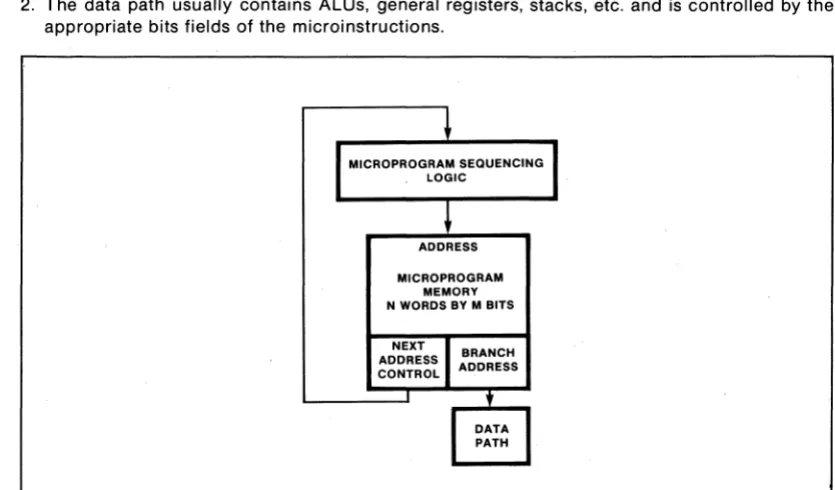
A microprogrammed system generally consists of two sections (Figure 1-1):
1. The controller section includes the microprogram memory and the sequencing logic required to provide the address to the microprogram memory. .
2. The data path usually contains ALUs, general registers, stacks, etc. and is controlled by the appropriate bits fields of the microinstructions.
MICROPROGRAM SEQUENCING LOGIC
ADDRESS MICROPROGRAM
MEMORY N WORDS BY M BITS
NEXT
I
BRANCH ADDRESS ADDRESS CONTROL .,
DATA PATH
[image:8.504.43.461.350.595.2]The microprogram memory is simply an N-word by M-bit memory used to hold the various microinstructions. Each word of the microprogram memory contains M bits, which are usually grouped into various fields. The field can consist of various numbers of bits. The definition of the various fields of microprogram word is referred to as FORMATTING. Figure 1-2 illustrates the format of a 32-bit microprogram word containing nine fields.
In general, a rrlicroinstruction must contain the following information: First, the definition and control of the operations to be performed by the data path and other system logic. These include such things as ALU function, ALU source, destination registers, shift or rotate control, stack operations, data in, data out select and so forth. Second, the address of the next microinstruction to be performed. In some cases, it can be implicit, such as when next address is current address plus one. In other cases, the actual value of the address field has to be supplied.
The use of microprogramming allows the designer to employ memory as one of the functional building blocks in logic design. Unlike hard-wired logic approach, where a designer generates timing and control signals by using combinations of gates and flip-flops and prays he does not have to make major changes in the future, microprogramming enables highly ordered and structured designs. Therefore, implementation of design changes is easier. Instead of tearing up gates and flip-flops, a change can usually be accomplished by reprogramming the control store. With memory prices dropping the way they are, the increased use of microprogramming in logic design is imminent. Microprogramming will be used in such applications as:
Special purpose controllers
High-speed (relative to MOS microprocessor) functions Extending compute~instruction sets
Emulations
Diagnosis/fault tolerance Multiprocessors
Multi-level hierarchies of processors Direct execution of high-level languages I/O controllers
FIELD DEFINITION
FIELD 1 - DATA IN CONTROL 2 - DATA OUT CONTROL
3 - ALU SOURCE OPERAND CONTROL 4 - ALU FUNCTION CONTROL 5 - ALU DESTINATION CONTROL 6 - CARRY CONTROL
7 - MISC. CONTROL 8 - BRANCH ADDRESS 9 - NEXT ADDRESS CONTROL
23 24 FIELD #8
Flg.1-2 Definition of 32-8it Microprogrammed Word Fields
Section 2
MICROPROGRAMMED SYSTEMS USING MACROLOGIC
The controller part of the microprogrammed system can be implemented using the 9408 Micro-program Sequencer. The 9408 is based upon a 10-bit Program Counter (PC) and addresses 1 K pages of microprogram memory (Figure 2-1). The basic instruction of the sequencer is FETCH, in which the program counter is incremented after each clock and, in effect, makes the next address the same as current address plus one. This type of addressing will cycle the microprogram memory sequentially, but will not be very adequate for most practical systems. The 9408 also has many provisions for branching.
The first type of branching is unconditional branching. Here a new address is placed on the 9408 input bus and loaded into the program counter. The new address can come from one of four different sources, selected by the BRVo to BRV3 instructions.
The second type of branching is conditional branching. Here the 9408 performs a test on one offour available inputs. If test conditions are met, the program counter is loaded with the address at the input bus (BRANCH). If the conditions are not met, the program counter is incremented (FETCH).
TO CONTROL
-BRANCH ADDR ESS LIFO STACK
10
CLOCK INSTRUCTIONS TEST FLAGS STROBE MULTIWAY INPUTS
I INCREMENTER
1-I
'+.
MULTI-PLEXER
t
TO CONTROL
- , " - PROGRAM COUNTER
t
TO CONTROL
9408 CONTROL
MULTI-PLEXER 1-- ...
PIPEt.NE CONTROL
VIA OUTPUTS INHIBIT
RESET
Flg.2-1 9408 Microprogram Sequencer
10
The third type is the multiway branch. The multiway branch is similarto an unconditional branch in that a program counter will always be loaded into a specified address, i.e., a branch is certain to occur. However, the address of the branch is determined by substituting the three least significant bits of the branch address present at the input bus by the value of three multiway (test) inputs. The result is that the branch will be made to one of eight different locations.
The fourth type of branching is subroutine branching. In branching to a subroutine, the incre-mented value of the program counter is loaded into the on-chip LIFO stack. Then, the program counter is loaded with the address at the input bus. In returning from a subroutine, the program counter is loaded with the contents of the top level of the stack.
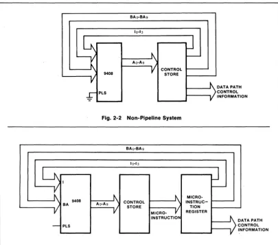
A microprogrammed system can be operated in either pipeline mode or non-pipeline mode. The non-pipeline controller is simply a 9408 and a control store (Figure 2-2). In a pipeline system, an edge-triggered microinstruction register is also needed (Figure 2-3). In a non-pipeline system, a microinstruction is read from the control store and executed before reading the next microin-struction. Since most microprogrammed systems are designed as synchronous machines, the maximum frequency the system will run at is indicated by the sum of the 9408 propagation delay (CP to address outputs), the memory access time, and the data path propagation delay.
BAo-BAg
10-13
~
~
Ao-Ag~
-V
CONTROL11
9408 STORE~
PLSFig_ 2-2 Non-Pipeline System
BAo-BAg
10-13
~I
K
9408~
-\
Ao-Ag CONTROL
11'
BA-V
STOREMICRO-
11'
INSTRUCTION-
PlSFig. 2-3 Pipeline System
2-2
J
I
- MICRO-
INSTRUC-TION REGISTER
DATA PATH CONTROL
NFORMATION I
J
r--R~N
ATA PATH ONTROl [image:11.505.43.448.241.598.2]In the non-pipeline system, the data path logic is idle during the part of the microcycle when the control store is being accessed. Similarly, the memory is not cycled and is sitting with the same outputs during the part ofthe cycle when the data path is used. A more efficient use of the resources will be overlapping the execution of the current microinstructions with the fetching of the next microinstruction. This requires holding the current microinstruction in a microinstruction register
(Figure 2-3). Here, the control memory access time is hidden from the data path propagation delay.
The system cycle time is the greater of the. sum of the propagation, set-up, and access times of the controller or the data path worst case propagation delay. In many instances, a microprogram written for a non-pipeline system cannot be executed in pipeline mode. However, the 9408 architecture is chosen so that the same microprogram can be executed in pipeline or non-pipeline mode without any modification. In the Macrologic Demonstrator, the 9408 is designed to work in the non-pipeline mode.
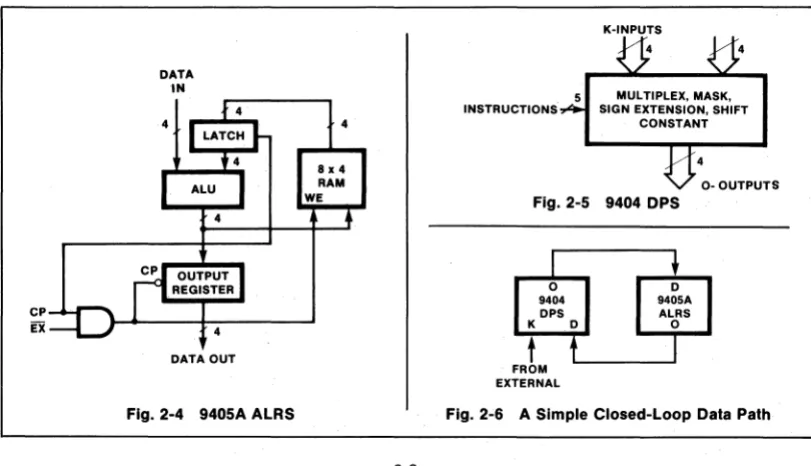
The data path logic generally consists of ALUs, general registers, stacks, etc., and can be readily implemented with Macrologic devices (ALRS, DPS, etc.). To provide logical, arithmetic and storage capabilities, the 9405A can be used (Figure 2-4). The 9405A is
a
4-bit slice containing an eight-function ALU, eight general purpose registers, four conditional code flags (carry, negative, zero, overflow), an output register and the necessary decoding logic. It can be expanded in multiples of four bits without additional components, or can be expanded with a carry lookahead unit for greater speed.Note the absence of a shifting network either before the RAM inputs or at the ALU outputs, which is quite common with other bit slice ALU designs. This is because Macrologic devices are designed to be functional building blocks in highly bus-organized systems so that sharing the input and output busses in the data path with the ALRS may be the hardware stack,general registers, etc. To eliminate the need for duplicating shifting capabilities in each Macrologic device, the shifting network is found in the 9404 Data Path Switch (DPS). The 9404 DPS is a combinational network consisting of two input busses and one output bus (Figure 2-5). It performs functions such as arithmetic or logic shifting, masking, sign extension and constant generations. In addition, when connected to other Macrologic devices (for example, the ALRS), it allows a closed-loop system to be formed, so that the output bus can communicate to the input bus. Figure 2-6 depicts a simple closed-loop system in which the ALRS inputs and outputs are connected to the DPS outputs and inputs respectively. External data may be introduced into the system usingthe K inputs of the DPS.
DATA IN
CP.-...,..-...
fi ~~----~---~
DATA OUT
Fig. 2-4 9405A ALRS
4
K-INPUTS
S MULTIPLEX, MASK, INSTRUCTIONS SIGN EXTENSION, SHIFT
CONSTANT 4
O-OUTPUTS
Fig. 2-5 9404 DPS
I
0 9404 DPS K
t
FROM EXTERNAL~
D 940SA ALRS
D 0
t
I
[image:12.504.49.455.396.629.2]As Macrologic devices are designed to be used in bus-organized systems, all devices are provided with 3-state data outputs and an Output Enable (EO) input to control them. Therefore, the data outputs from the devices can be bussed together to obtain the output bus (D-bus) as in Figure2-7. With a LOW level on the appropriate
(E<:»
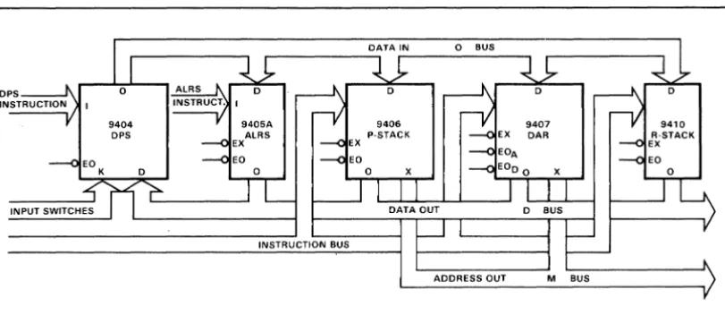
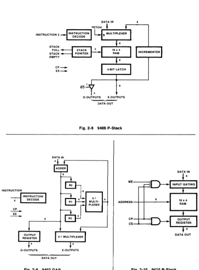
input, a Macrologic device can be made to source data onto the output bus. The data inputs of the Macrologic devices can also be bussed together to obtain the input bus. Except for the DPS, Macrologic devices used in the data path are provided with individual execute (EX) input and a device will not respond to the clock unless its EX input is LOW. Thus, the instruction inputs can be bussed together to obtain an instruction bus. The result is that during a single clock cycle, information can be routed from any device in the data path to any other device (including itself) by controlling the proper EX and EO inputs.For some applications, a DPS and ALRS combination in the data path provides enough storage and computing power. For example, in an emulation design, one of the eight registers in the ALRS can be treated as the program counter, four can be accumulator registers, and the other three can be scratch pads. In some applications, this may be inadequate. If, for example, the emulation is for a machine with macrosubroutine nesting capabilities, the 9406 program stack can be added into the data path (Figure 2-8). The 9406 is a 16-level, last-in first-out hardware stack. The top of the stack can be used as the program counterand the other levels provide return address storage for nested subroutines. In addition, it provides two status outputs to indicate Stack Full (SF) and Stack Empty (SE) conditions.
But suppose someone needed more than 16 levels of stack, say for unlimited levels of subroutine nesting capability. In that case, fixed level hardware stack will not meet the requirement. The approach may be changed to put the stack out in RAM (Random Access Memory) and maintain it by pOinters. The 9407 Data Access Register can be used for this purpose (Figure 2-9). Basically, the 9407 contains three registers with an adder network, an output register and a two-to-one multi-plexer to select either the adder output or the individual register output. It is designed to perform memory address functi6ns for RAM resident stack type applications. For example, the three registers can be used as program counter, stack pOinters and operand address. The 9407 implements 16 instructions, which allows pre- or post-increment/decrement and register-to-register transfer in a single clock cycle. For applications which require more storage capacity than the eight registers the 9405A provides, the 9410 register stack (R-stack) can be added to the data path. The 9410 is a high speed 16-word by 4-bit memory with an edge-triggered output register
(Figure 2-10).
Fig. 2-7 Bussing Macrologic Arrays
[image:13.507.49.455.414.590.2]CP
-
EX-INSTRUCTION 2
STACK FULL STACK EMPTY
DATA IN
O-OUTPUTS X-OUTPUTS DATA OUT
Fig. 2-9 9407 DAR
4
O-OUTPUTS X-OUTPUTS
-
DATA OUTFig. 2-8 9406 P-Stack
4
4
DATA IN
W E - - - - < l , '
3-1
MULTI-PLEXER
ADDRESS-~~-_~-~~
Cp-+-.+--oIr""
CS --6----<lL.-J
DATA OUT
[image:14.507.50.455.57.606.2]A SIMPLE PROCESSOR EXAMPLE
One of the many possible Macrologic applications is to implement emulators for existinginstruc-tion sets. These complex funcexistinginstruc-tional LSls offer improved cost and performance while retaining software compatibility with the target machine. A simple 16-bit processor is a good example to demonstrate the ease of use and versatility of Macrologic.
The 16-bit fixed word-length processor, with four accumulators (ACo-AC3) and 2's complement arithmetic, has a 16-word push/pop stack for subroutine nesting, as well as general use. The memory reference instruction format is shown in Figure 2-11. The 2-bit index field in the instruction
specifies four addressing modes - base page, PC relative, AC2 and AC3 relative. For the base-page mode, the 8-bit displacement field of the instruction is taken as the absolute address, i.e., first 256 memory locations. For the relative mode, the 8-bit displacement is treated as a signed number in 2's complement notation and added to the Program Counter (PC relative) or one of the specified accumulators (AC2 or AC3 relative). The result is then used as the effective address for the operand.
A data path suitable for this processor is shown in Figure 2-12. It consists of a bit ALRS array,
16-bit P-stack array and 16-16-bit DPS array. The ALRS and DPS can perform all the arithmetic logic operations needed. The P-stack provides the required 16-level stack function. The ALRS has eight built-in accumulators, but only four are needed for this processor. The P-stack has the necessary features to implement the PC; however, if this feature is used, only 151evels of nesting remain. This processor requires 16. Because the ALRS has four spare accumulators, one of these can be used as the PC, leaving three spares. Thus the PC feature of the P-stack is not needed and the address outputs are not used. The storage in the ALRS is allocated as follows: Ro = ACo, R1 = AC1, R2 = AC2, R3 =AC3, R4 = PC, Rs =TEMP 1, R6 =TEMP 2and R7 =TEMP 3. An edge-triggered Memory Address Register (MAR) on the output bus is provided. Data from the memory is introduced into the data path using one of the input ports of the DPS array. Data tothe memory is obtained directly from the output bus. An edge-triggered Instruction Register (IR) is also provided to hold the OP code bits and index bits of the macroinstruction.
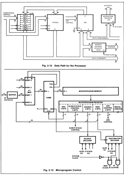
Figure 2-13 illustrates the microprogram control section for the data path. This control is centered
around the 9408 sequencer operating in the pipeline mode. The INH output of the 9408 is used to share the control fields. Thus, the source, destination, and ALRS/P-stack control fields provide the 10-bit address for branching when needed. A 6-bit DPS control field provides the instruction inputs for the DPS array while the 4-bit SEQ field provides the instruction inputs for the 9408. Other fields lumped as miscellaneous are used to control the memory, etc.
The source and destination fields are decoded to activate the EO and EX inputs (see Figure 2-13).
Note that the IR clock and MAR clock signals are generated by gating the system clock with the appropriate destination decoder outputs. The Branch Address inputs (BAo-BAg) are obtained from a
15 14 13 12 11 10 9 8 7 6 5 4 3 2 1 0
I
I I I I I
~P
CODEI
INDEXI
I
I I I I I I I
DISPLACEMENTI
Fig. 2-11 Memory Reference Instruction Format
[image:15.505.41.457.493.597.2]ALRS/P-sTACK CONTROL
10
10
ALRS
PORT 2
4:1 10 MUX
PORTO Vee
10
CONTROL DPS
Fig. 2-12 Data Path for the Processor
VIA. VIA,
IR OUTPUT
INSTRUCTION REGISTER
ORI CP
t
IA CLOCKDATA FROM MEMORY
BAo-9 10 Ao-9 MICROPROGRAM MEMORY 4708B
PLS
ALRS/P-STACK CONTROL
ALRS P·STACK EO EO
Fig.2-13 Microprogram Control
P-STACK EX
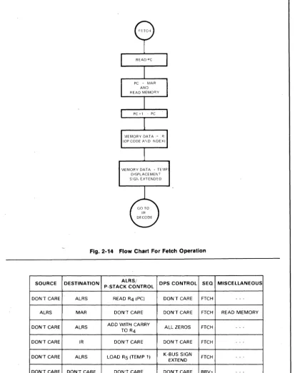
[image:16.504.41.456.32.622.2]4-way input multiplexer which, in turn, is controlled by the VIAo and VIA1 outputs of the 9408. One of the inputs to this multiplexer qonsists of the address inputs for branching from the microinstruction register. The second part is fed by a mapper that may be a PROM or FPLA. It receives the IR outputs and translates them into a starting address in the control memory for emulation. Figure 2-14 is a flow chart for the sequence of operations to accomplish macroinstruction fetch, while Table 2-1 lists the operations performed by various data path elements and the 9408.
The first operation is to read the PC. Thus, the destination field specifies the ALRS and the destination decoder drives the EX input of the ALRS LOW. The ALRS/P-stack control field specifies "Read R4." At the end of the microcycle, the contents of R4, i.e., the PC, are in the output register of the ALRS. The SEQ field of the first microinstruction is FETCH; therefore, the 9408 generates the address of the second microinstruction.
Here, the ALRS is specified as the source and the MAR as the destination. The source decoder activates the EO input of the ALRS, the destination decoder enables the gating for the MAR clock, and the microinstruction loads the PC into the MAR. In the miscellaneous field, a memory read is initiated. The third microinstruction is made to increment R4 by selecting ALRS as the destination specifying Add with Carry. The DPS outputs (ALRS inputs) are forced HIGH. This incrementation is in preparation for the next macroinstruction fetch. The result from the memory read operation, initiated during the second microinstruction, is now available on the K-bus of the DPS. The fourth microinstruction activates the IR clock so that the eight most significant bits of the memory data are loaded into the IR. Assuming the data is still on the bus, the sign extended displacement is loaded into R5 (TEMP 1) of the ALRS in the fifth microcycle by selecting "Load R5" as the ALRS operation, and selecting the "K-Bus Sign Extended" for the DPS. It should be recalled that the data path has 16-bit fixed word length and the displacement must be treated as a 2's complement number. By using the sign extension capabilities of the DPS, the sign bits, i.e., most significant bits, can be aligned. At this point, the instruction is in the IR and the sign extended displacement is in TEMP 1. The sign of the least significant eight bits of the macroinstruction is extended in anticipation of a memory reference instruction. The sixth microcycle is intended to decode the I R. By specifying a BRV1 in the SEQ field, the VIA outputs of the 9408 select the mapper output as the source for next address. The mapper is designed to provide the starting address of the routine to emulate the instruction currently residing in the IR.
The total microprogram really consists of several simple routines. These easy steps can be converted into binary patterns to be loaded into the control store. Once a data path architecture and microinstruction format has been chosen for a given system deSign, the microprogram can be written to realize the desired function. It can then be assembled, using the microprogram assembler, to get the binary listing that specifies the control store address and contents. Using this information, the control store can be loaded with the program and the system is ready for operation.
SOURCE
DON'T CARE
ALRS
DON'T CARE
DON'T CARE
DON'T CARE
DON'T CARE
MEMORY DATA -> TEMP
DISPLACEMENT
SIGN EXTENDED
Fig. 2-14 Flow Chart For Fetch Operation
DESTINATION ALRS/ DPS CONTROL SEa
P-STACK CONTROL
ALRS READ R4 (PC) DON'T CARE FTCH
MAR DON'T CARE DON'T CARE FTCH
ALRS ADD WITH CARRY ALL ZEROS FTCH TO R4
IR DON'T CARE DON'T CARE FTCH
ALRS LOAD R5 (TEMP 1) K-BUS SIGN FTCH EXTEND
DON'T CARE DON'T CARE DON'T CARE BRVl
Table 2-1 Operations for Fetch Instruction
MISCELLANEOUS
-
--READ MEMORY
-
-
---
[image:18.507.49.463.49.573.2]--Section 3
DESCRIPTION AND OPERATION OF THE MACROLOGIC
DEMONSTRATOR
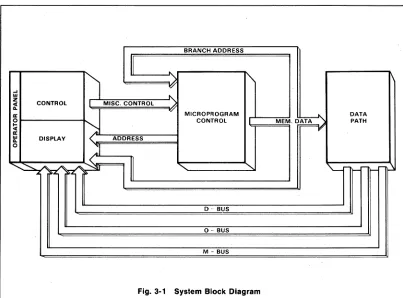
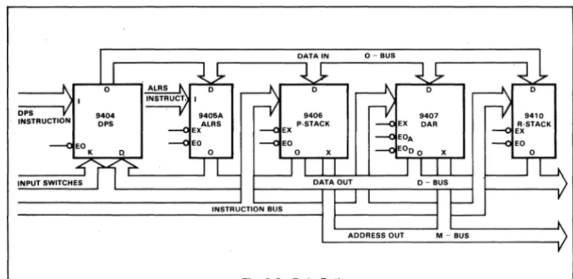
The Macrologic Demonstrator is an educational tool designed to familiarize the user with the processor-oriented devices in the Macrologic family. It consists of three main functional blocks (Figure 3-1). The 8-bit wide data path contains an ALU, a register file,UFOstack and miscellaneous logic. The microprogram controller contains the control memory, as well as microprogram addressing and sequencing logic. The operator panel provides the human interface and allows the operator to load and modify the control memory, run or single-step the microprogram and look at system status and contents of various system busses. An S-100 bus interface is also provided for optional automatic loading of the control store by 8080 based system.
Schematics for the Macrologic Demonstrator are located at the end of this section.
THE DATA PATH
Two 4-bit slices of the following Macrologic devices form the 8-bit wide data path (Figure 3-2). The Data Path Switch (9404 DPS) allows shifting, constant generation and other operations. An Arithmetic Logic Register Stack (9405A ALRS) performs eight arithmetic and logic functions and includes eight data registers. The Program Stack (9406 P-stack) contains a 16-level stack for last-in, first-out storage. TheData Access Register (9407 DAR) includes three general purpose registers and an adder network which can be used for RAM-resident stack-type functions. A Register Stack (9410 R-stack) provides 16 words Of high-speed read/write memory for scratchpad area.
BRANCH ADDRESS
II
...
J
)'\
...
IVw
...
Z
CONTROL MISC. CONTROL
f
~
vII: MICROPROGRAM
MEM.D~ DATA
0 CONTROL PATH
l-e( IP"
II:
w DISPLAY
<
ADDRESSIL
0
;1
<
\I
~A~~Ar-
"
"-
'--
r-
-0 BUS 0 - BUS M - BUS
[image:20.503.50.453.309.607.2]The data path illustrates the highly bus-organized configuration possible with Macrologic systems. The instruction inputs of the P-stack, OARs and R-stacks are bussed together to allow instruction field sharing. That is, the same 4-bit field (C4-C7) is used to control the devices, but only one of these devices is allowed to execute an instruction in a microcycle. The K-bus inputs of the OPSs are tied to the eight data input switches on the operator panel so external information can be introduced into the data path. Three other busses are also available - the O-bus, a-bus and M-bus. The O-bus is created by connecting the O-inputs of the OPSs to the corresponding a-outputs of the ALRSs, P-stacks, OARs and R-stacks. The a-bus is the result of connecting the a-outputs of the OPSs to the corresponding D-inputs of the ALRSs, P-stacks, DARs and R-stacks. The M-bus is created by wiring the X outputs of the P-stacks to the X outputs of the DARs.
Except for the DPS, all Macrologic devices in...!!:)e data path are clocked by a common system clock. Each of these devices has an Execute input (EX) and the device will not respond to the clock unless (EX) is LOW. In addition, the 3-state outputs of the devices remain in the high impedance state except when the Output Enable (EO) is LOW. Thus, during a single clock cycle, information can be routed from any device in the data path to any other device (including itself) by controlling the proper EX and EO inputs.
The manner in which the individual EX and EO inputs of the Macrologic devices are controlled is shown in Figure 3-3. Bits 0 and 1 of the microprogram control word (CO and C1) are address inputs
to an LS1391-of-4 decoder. Its active LOW outputs are tied to the Output Enable (EO) inputs of the ALRSs, DARs, P-stacks and R-stacks, respectively. Therefore, a device can be selected to source data on to the Data Out bus (D-bus) in a clock cycle by appropriately selecting bit 0 and bit 1 of the microprogram control word. Similarly, bit 2 and 3 (C2, C3) of the microprogram control word are inputs to the other half of the LS139 package. Three of the four active LOW outputs are tied to the Execute (EX) inputs of the DARs, P-stacks, and R-stacks, respectively. Thus, bit 2 and 3 can select one of these three devices to be active and respond to input clocking, or none of them to be activated during a clock cycle. The ALRSs are operated in the general register mode. A two-to-one multiplexer routes the A field inputs of the 9405s to the source and destination registers during the HIGH and LOW periods of the clock respectively. The 10 input of the most significant ALRS slice is used both to pass instructions and carry information from the least significant ALRS slice.
Fig. 3-2 Data Path
[image:21.505.42.455.399.600.2]To extend the shifting capability in the data path, atwo-to-one multiplexer selects data, originating from either a bit in the control memory (C30) or the right and left serial DPS outputs, and enters it into the left and right serial inputs of the DPSs (Figure 3-4).
The select input of the two-to-one multiplexer is controlled by a rotate select bit (C14). If this bit is HIGH during a right shift, the right serial output is shifted into the most significant DPS position which, in effect, makes the instruction a right rotation. For left rotation, the left serial output is shifted into the least significant DPS position. If the rotate select bit (C14) is LOW, then the value of the left or right shift carry in is under microprogram control and determined by control word bit 30 (C30). If C30 is HIGH during a right shift, a "0" will be shifted into the most significant DPS position since the DPS has active LOW inputs.
MICROPROGRAM CONTROL
The microprogram memory is constructed using eight 1 K 93L422 fully decoded RAMs organized as 256 words by 32 bits. A 9408 Microprogram Sequencer provides address inputs to the control memory (Figure 3-5).
o , 2 3 4 6 6 7 8910 11 12 13 '4 ~BRANCH ADDRESS~ 15 16 17 18 19 20 21 22 23 24 2526 27 21 2. 30 3'
I
SOURCEI
I
9406,07.10,1 9404,I
DESTINATION INSTRUCTIONS INSTRUCTION ROTATE Ry
I
RxI
INSTRUCTION 9405AI
INSTUCTION 940SI I I I I
-
-.
~
MISC .SINGLE CONTROL
STEP
I.
I,. 11bllc lOa lOb IOc!
I
ep ( 9lS157
-::!O. A la lb Zc lei
-=-I
E AD A,I
I
E AD A,
I
IDECODER DECODER
03 02 0, 00 03 02 0, 00 I
I~ I~ I~ I~
II II II II
I I I I Ir
12 A2 A1 AOI
~:2
A2 A, ADI
..
..
a:..
"
..
a:...
I" 940SA 9405A...
...
..
~ :;; .....
)( e22 I,..
..
C..
C w~ID ALRS ALRS
a:
..
..
a:..
- I - MSS lOW LSB
FROM CONTROL
WORD
e2'
Fig. 3-3 Data InlOut Select and Address Multiplexing in ALRS
C30 EXTERNAl LEFT/RIGHT CARRY IN
I
h. lOa lOb I'b
C14 S 9LS157
2·1 MULTIPLEXER Zb Za
I I
Lo
9404 RI LO 9404 RI
P--L-...o LI DPS Ro LI DPS Ro [image:22.504.47.459.215.598.2]The clock input of the 9408 is a signal called SEQCK, which is the same as the system clock (CP) that goes to all other Macrologic devices in the data path when the system is in the Run or Single-Step mode. When the system is in the Halt mode, SEQCK is held HIGH and only goes LOW momentarily when either the Address Load switch is depressed, or the Deposit Next or Examine Next switch is depressed and Field Select (FS1 and FSo) is "11" (to be described later).
The 9408 Bran,ch Address inputs come from the outputs of two LS157 two-to-one multiplexers whose select input is tied to the VIAo output of the 9408. A Branch VIAo instruction will select control memory bits 16 to 23 (C16-C23) as the branch address, whereas the Branch VIA1 instruction will load the microprogram address from the control panel input switches. Actually, the 9408 has the capability of selecting its branch address from up to four different sources through the BRVo to BRV3 instructions. But in the Demonstrator design, only two branch address sources are implemented.
The Multiway switches (MO to M2) on the control panel feed the 9408 MWo-MW2 inputs for multiway branching. The four ALRSs status flags (zero, overflow, carry and negative) are strobed in the 9408 internal test register at the end of each microcycle in which the ALRS,s are exercised by an active LOW signal called ALUEXL which also goes to the Execute (EX) input of the ALRSs. The PLS (Pipeline Select) input is grounded for non-pipeline operation.
.moor
FLAGS X FROM Y ALRSZ
ALUEX
BA
CONTROL ~ DATA STORE SWITCHES
~ 8 ~ 8
9LS167
sJ-2-1 MUX, MW SEQ CK~ SWl
r3 HES }'8
~P MvvO-2 B 0-9
T3 VIAO
-•
T2 VIA1-•
T1 9408 10-3 4,,
TO STRB
MR PLS A -9 INH
MR
J.
DIS!BLE - 10
~ ALRS
CONTROL STORE
256 x 32
~
I~20
I
DATA PATH
10 4 , 9LS153
,
4-1 11 4,
,
Z MUX4, 12 I
SOl3 4, S1
t
t
RUN ADDR/DATA LOAD , 4
,
"-BRV1 FTCHI
FROM MICROPROGRAMFig. 3-5 Microprogram Memory and Sequencing Logic
[image:23.503.52.456.247.596.2]The instruction inputs of the 9408 come from the outputs of two LS153 four-to~one multiplexers.
Table 3-1 depicts the manner in which the various combinations of the instruction inputs are
selected. In the Run or Single-Step mode, S1 of the multiplexer select input is HIGH and the 9408 instruction inputs are entered via the microprogram control memory output bits 24 to 27 (C24-C27). In the Halt mode, S1 of the multiplexer select input is LOW and So of the multiplexer input causes the 9408 to either increment the microprogram address by one (FETCH) or load the microprogram address from the controlpanel input switches (BRV1) when the 9408 is clocked. Normally, the clock input of the 9408 is disabled (held HIGH) and the So input of the LS153 is HIGH, forcing the FETCH instruction of the 9408 instruction inputs. When Field Select (FS1 and FSo) is "11" and either the Examine Next or Deposit Next switch is activated, the 9408 is clocked once. This increments the microprogram address by one, allowing the next control word to be examined or loaded. Operation of the Load Address switch momentarily brings the So input of the LS153 LOW, forcing the BRV1 instruction on the 9408 instruction inputs, and selects the input switches as 9408 Branch Address inputs. The 9408 is again clocked once to match its address outputs to the input switch data.
OPERATOR PANEL
The operator panel consists of two sections - control and display. The control section provides the operator interface to the control memory and data path through a number of toggle switches. The display allows the operator to monitor the microprogram address and data, ALU status flags and the various system busses through LEOs. In addition, a number of turret terminals are provided to allow easy access to some important system signals.
Display
The display consists of two rows of eight LEOs which read the microprogram address and data; a row of eight bus status LEOs, four ALU status LEOs, two Field Select LEOs and a RUN indicator LED. Since the microprogram control word is 32 bits wide, two control inputs (FS1 and FSo) select four separate fields to be displayed by a single set of eight data LEOs. Setting FS1 and FSo to "00" produces the left most (most significant) eight bits of a control word. A setting of "01" produces the next eight bits, "10" the next, and "11" the right most (least significant) 8-bit field. The ALRS flags (zero, negative, carry and overflow) are latched into the four status LEOs so that ALU status can be continuously monitored.
Control
The panel control section, contains a group of eight toggle switches (SWO-SW7l for Branch Address or Data input to the system, as well as a number of miscellaneous control switches. The Clock Select switch selects between an internal 2 MHz oscillator or an external clock provided by
S1
0 0
1 1 S1 -0
S1 = 1
So = 0 So = 1
So 13 112
I
11I
100 .0 1 0 1
1 0 0 1 0
0 C24 C25 C26 C27} 1 C24 C25 C26 C27 Halt
Run or Single Step Address Load Data Load
MEANING BRV1 FETCH Controlled by Microprogram
[image:24.504.48.451.460.590.2]the user. If an external clock (such as a pulse generator) is used, it should be attached to the EXT-ClK IN turret terminal on the board. A group of three Multiway switches (MO-M2) provides the multiway inputs to the 9408 for eight-way branching. Two Data Bus Select switches (DS1, DSO) select either a lamp test or the contents of one of three system busses (0, D, or M-bus) for display by the eight data-bus lEDs as illustrated by Table 3-2. The Master Reset switch halts the system and clears the microprogram address and field to zero.
The Run/Halt switch is a 2-function toggle switch that selects either the Run or Halt mode. If the processor is halted, pressing this switch returns the processor to the Run mode. The processor then executes the microprogram beginning with the instruction contained in the memory location pOinted to by the microprogram address. It continues in this fashion until the Run/Halt switch is pressed again; however, the processor halts only after completion of the current microinstruction.
While the processor is in the Halt mode, a number of other switch functions can be activated. The load Address switch loads input switch data as the microprogram address. The Deposit switch writes the 8-bit words, at the input switches, into the field of the memory location addressed by the 9408 address and Field Select (FS1 and FSo) outputs. The Deposit Next switch operates similarly to Deposit; however, the field is incremented by one before the input switch data is written into memory. Moreover, if Field Select is "11," the field is recirculated to "00" and the 9408 address outputs are incremented by one before the input switch data is written into memory. Thus, the user can load a microprogram eight bits at a time without laboriously loading addresses by repeatedly setting up data switches and then pressing the Deposit Next switch.
The Examine Next switch displays the data in the next field by lighting the appropriate lEDs, and allows the operator to examine memory data field by field and location by location. The micro-program address lEDs display the memory location of the next processor instruction. Pressing the Single Step switch executes that instruction and then halts the processor. The Single Step switch is especially useful in program debug.
A number of turret terminals provide convenient access to some system signals as test points for viewing on the oscilloscope. The CP test point connects directly to the system clock line of the Demonstrator and represents the actual clock signal applied to the Macrologic devices in the data path. The AlUEXl test point is the lOW active signal which goes to the Execute (EX) input of the AlRS. The ADDR SYNC test pOint outputs a HIGH pulse whenever the microprogram address matches the input switch word. In this manner, the input switches can be used to select the microprogram address at which a sync pulse is desired. This provides a handy signal for use as a reference trace on the oscilloscope and signals in the vicinity of the synchronized instruction can be examined by placing the microprogram in a loop. The C31 test point is tied directly to control word bit 31, which is a spare bit at this time. However, it can be used as an additional marker to identify a microinstruction or provide another reference signal on the scope. A Ground point is also brought out to a turret terminal next to the ADDR SYNC test pOint so that the ground clip of an oscilloscope probe can be attached to it.
DATA BUS SELECT BUS SELECTION
DS1 DSO
0 0 O-Bus
0 1 D-Bus
1 0 M-Bus
1 1 Lamp Test
Table 3-2 Data Bus Select Switches Operation
[image:25.504.59.454.507.593.2]CONTROL WORD FORMAT
Choosing the width and format of the microprogram control word is a task which involves tradeoff between system performance and memory cost. A format which dedicates separate fields for each individual control function allows many independent operations to be done in one microcycle but also yields the widest control word. Usually, some sort of field sharing is implemented to reduce the control word width without sacrificing too much performance. The Macrologic Demonstrator uses a 32-bit control word reduced by the following overlapping and encoding techniques.
The control inputs for the ALRS and the Branch Address inputs of the 9408 are overlapped since most program structures consist of more fetches than branches. The address for the 9408 Microprogram Sequencer is implicit during Fetch (FTCH) and Return from Subroutine (RTS), which suggests that the branch address field of the 9408 can be overlapped with the instruction input field of another Macrologic element in the system. In this case, the 8-bit branch address field can be conveniently shared with the instruction and register fields of the ALRS. The 9408 Inhibit (INH) output simplifies field overlap; the EX input of the ALRS is simply disabled except during a FTCH or RTS.
Since the O-bus is 3-state, only one of the four Macrologic elements can drive this bus at any time. Thus the four O-bus sources can be encoded by two bits. Since the likelihood is sma" that more than one Macrologic element in the system wi" need to operate on the same input during the same microcycle, the four D-bus destinations can also be encoded by two bits. Actua"y, there are only three Macrologic device destinations and four possible permutations of two bits, which leaves a 'free' state "00." This state can be used to select an external device or to deactivate a" three Macrologic elements. Note that the ALRS execution is controlled by the INH output of the 9408 and is unaffected by this field. The result is a 32-bit control word with field definition as shown in Table 3-3.
BITS FUNCTION
CO-C1 O-bus source. These bits select the device driving the input bus of the DPS by activating the proper Output Enable (EO) input. "OO"-ALRS, "01"-DAR, "10" P-stack, "11"-R-stack C2-C3 D-bus destination. These bits specify device to be activated and respond to C4 - C7 by enabling
the proper Execute (EX) input. "00" - EXT', "01" - DAR: "10" - P-stack, "11" - R-stack C4-C7 Shared between P-stack, DAR and R-stack, these bits are Instruction inputs to the P-stack and
DAR and Address inputs to the R-stack. C8-C13 Instruction inputs to the DPS.
C14 Rotate control. Specifies source of carry in (external or rotate) during DPS shifts. C15-C23 Shared between the 9408 Sequencer and ALRS. When the 9408 instruction (C24 - C27) is
neither a Fetch or a Return, these bits are the Branch Address. Otherwise, C15 - C17 select one ALRS register for destination of ALU operations, C18 - C20 select one ALRS register as source of ALU operations, C21-C23 become ALRS Instruction inputs.
C24-C27 9408 Sequencer Instruction inputs.
C28 9407 X-bus enable input. When the 9406 is executing a FETCH instruction, C28 should be held HIGH for microcycle to prevent both the 9406 and 9407 from driving the M-bus at the same time. C29 9406 and 9407 carry in input.
C30 9404 carry in input for shift function. If rotate control (C14) is LOW, the value of C30 (active LOW) will be shifted into the least o"r most significant pOSition of the DPS following a left or right shift, respectively.
C31 Spare. This bit is brought out to a turret terminal and can be used as a marker to identify one or a group of microinstructions.
[image:26.503.50.457.311.606.2]MISCELLANEOUS
The Demonstrator is pretty much self-contained. The only additional equipment needed for its operation is a 5 V power supply capable of delivering about 2 A of current to be attached to the Vee and GND turret terminals in the lower left hand corner of the board.
Instead of hand loading the microprogram through input switches, a user who has an S-100 bus 8080 based system can choose to have the control store of the Demonstrator loaded by the 8080. The Demonstrator card edge connector plugs directly into the S-100 bus. A JLA7805 voltage regulator in TO-220 package is used to obtain Vee from the 8 V which come from pin 1 of the S-100 bus. A 5
n,
2 W resistor is required between the input and outputterminal of the regulatorto provide enough current for the board.OPERATING PROCEDURE FOR CONTROL PANEL OF MACROLOGIC DEMONSTRATOR
The following operations are possible when the system is in the Halt mode. To place the system in the Halt mode, use either the Run/Halt switch or press the Master Reset switch momentarily.
Loading In Microprogram
1. Press Master Reset. Make sure system is in Halt mode by verifying Run light is off. 2. Set up starting address via the eight data input switches.
3. Hit Load Address switch momentarily and verify the address lights show the same data as the input switch settings.
4. Verify Field Select (FS1 and FSo) Iights="OO." Set up data for first field in data input switches. 5. Depress Deposit switch and verify the data lights show the same data as the input switch
setting.
6. Set up data for the next field through the input switches. 7. Depress Deposit Next switch and verify:
a. The Field Select (FS1, FSo) lights are incremented by one.
b. If the Field Select lights =:'11," the address light will be incremented by one and the Field Select lights will go to "00."
c. The data lights are the same as the input switch settings.
8. Repeat steps 6 and 7 to input data sequentially, field by field, location by location.
Verifying Program
1. Press Master Reset to get into the Halt mode.
2. Set up desired starting address of microprogram by input switches. Press Load Address switch momentarily and verify the address lights show the same data as the input switch settings.
3. By continuing depressing the Examine Next switch, one can sequentially examine the contents of the microprogram, 8-bit field at a time, location by location.
Modifying Program
1. Hit Master Reset to clear out address and field lights.
2. Enter starting address via input switches and depress Load Address switch. 3. Get to desired field using Examine Next switch.
4. Verify old data is displayed on data lights. Set up new desired data through input data switches.
5. Hit Deposit switch and verify new data is deposited.
6. Repeat above steps for other fields to be modified or use Examine Next switch to advance to the next field to be modified and repeat step 4 and 5.
Single Stepping Microprogram
1. Make sure system is in Halt mode. Set up starting microprogram address via the eight data input switches.
2. Press Load Address switch and verify the address lights display the same data as input switches.
3. Depressing Single Step switch momentarily will cause the microinstruction pointed to by the microprogram address LEDs to be executed. The system will then be halted.
4. Repeat step 3 to execute the microprogram one microinstruction at a time.
Running the Microprogram
1. Set up starting address via input switches and hit Load Address switch.
2. Depress Halt/Run switch and the RUN light will come on, verifying the system has begun execution starting from the microinstruction specified in the microprogram address.
Loading the Microprogram Memory Through the S-100 Bus
The Macrologic Demonstrator has the provision for an S-100 bus system to load its control memory. The write signal from the 8080 Processor (PWRL) is simply made to act like the Deposit Next switch. The Demonstrator board decodes the two higher order bits of the 8080 address bus and makes sure they are equal to "11" before its control memory is loaded, i.e., the Demonstrator can have a hexadecimal memory address of CXXX up to FXXX. To load the microprogram memory, 8-bit field at a time, do the following:
1. Halt the 8080 system. Plug the Macrologic Demonstrator into the S-100 bus connector. 2. Press Master Reset and verify the address and field lights are zero and the system is halted. 3. Set up the starting microprogram address via the input switches and press the Load Address
switch.
4. Set up the first field of the microprogram through the input switches. Depress Deposit momentarily. Verify the data lights are the same as the input switch settings.
5. Put all eight data switches in the Up position.
6. Any subsequent write by the 8080 Processor to memory address CXXX through FXXX will increment the field by one first before writing the data, i.e., it generates the same action as if the Deposit Next switch is depressed.
V"
RUN/HALT
Vee
Vee
MASTER RESET
Vee Vee DEPOSIT NEXT Vee Vee DEPOSIT Cf'
~ au
0 Vee
Hll
.
Vee
LOAD ADDRESS
Vee
Vee
SINGLE STEP Hil
, Vee
lkJl 15
Vee
EXAMINE NEXT
Vee
R' 33011
®
e
PWRl RUN V" RUNl MRL 14 LSOI "' DEPOSIT NEXTl® ® ®
SOUT SINPBOARO ENA8lEL SII,2W Vee ®OOl 10
@OOS 4
@OO4
"'
LS3678
003.,
10
@OO2
@OOl 4
@)ooo
,
1
.,
LS36762DECOUPLING
CAPACITORS O.OljJ.F
Fig. 3-6 Macrologic Control Panel Switches Schematic
SW'
SW'
SW.
SW'
Vee
CLOCK MW,
SEL
NW1
[image:29.649.37.607.43.431.2]SYS CLOCK
MAL
ADDRESS LOADl FS11 CP
DEPOSIT NEXTL EXAMINE NEXTL
DEPOSITL
SYS CLOCKL
A10 12 PA
£0
Or-LS74
.... LS20 Fa B
LS04
10 I 11 B
~~GB
12 E2~ CK CLA ~
13.~ 7
...
1'3 Yee
9 3j4j5iB
*
7 PE Po p, p, P3
~ CEP
10 LS161 TC
'2
CETG2 r--'5 CP
MA 00 Q1 0203
1 14 13112111
LS04
~
11 Jo.. 10 4 F3 LSS1 LSOB -':": _ 6 5"";;';";'; 6 13,,!;!2t 3 4 H2 12 H2 2
11 Yee
16'
)3 )4 )5 )6*
13~ 11 7 PE Po p, p, P3
12 G3
~
CEP--
1 2 CET lS161 F2 TC r-'S2 G3 CP lSDO
_ 3
MA 00 Q1 02 Q3
~8 9 G3
3 '
14 13112111--
Yeel~
"lk
o'"---h
E2 6 I H22~ LSO~ ~3
LS~~~~
1'-1 2 3 G5
'7
E Ao A, 4 B
LS139
~
:::;~
E4
•
9000102 03 11 11 33Dll 330!1
4 S 6 7
Fig. 3-8 Examine, Deposit, and Address Load Logic Schematic
SE~ CK
FSO
FS11
FS1
Vee WRITE OL WRITE 1l
WRITE 2L
[image:31.650.44.607.47.445.2]C27 CH C25 CM CU CD C21 C20 Cl1 Cl1 C17 Cl1 CIS C14 Cl1 C12 Cll Cl0 COl COl C07 . COl
'"
COl.!.
'"
CMCOl
COl
COl
COO
10
I",
12 13 615 4 3 6 5 4 3 10 11 12 13~
140!.r
-14 10. 11. 120 130 lOt. lIb 120 13b
r - - So
LS153 LS153
~
2 D66!
-DS
2
- S, Za
9 7 9
14
r -2
-C28 C28
10 11 12 13 6 5 4 3
1
G5'"
7
~:2
LS1S3
E6
:::1~~~~
1 330 U
LS
04 2
.,~ FLY
-""'110
3 330 n
14
r -2
-C30 C31
6 S 4 3 10 11 12 13
LS153
D8
4 330 U
S
"'7
LS04
6
- ; : , FLY
- - 110
5 33011 en· i
Cn~4 Cn·S Cno6
L---~~4_---~----~~~---~4_---~~---~4_---~~~---~---Ycc
[image:32.647.37.613.37.442.2]Cf
~
..,.
M7 MO MO M. M3 M2 M1 MO D7L DOL DOL D4L D3L D2L D1L DOL D7L OIL DOL D4L D3L D2L
on
OOL
DSO DS1
Yee
10
'0.
~So
~ 5,
0 • 13 1,0 11 12 )13
11, '2, 13i1 lOb 11, '2, '3, LS1S3
.3
z, z,
7
•
:::2
~ ~~:
:::2~J1 J1
33O!! 33011
,.
•
I
1,0 11 12 1,3
•
0 • I.•
0 • 13 10 11 12 1,3 10 11 12 113•
0 • J3'0. 11, '2, 13& lOb 11, 12b 13b '0. 11" 12a '3, '0. I1b 121, '3, 10, 11, '2, '3, '0. 110 12t> '3,
~ ---.:!.! So o!.. ~
..
o!.. ~.0
p!-LS1S3 LS153 LS1S3
~ ~ 5,
••
o!!•
s, .0 o!!• s, .0 p!!
Z. z, Z. z, z, Z,
•
7 7•
•
7:::2
~
:::2~ :::2~ :::2~ :::2~ :::2~J1 J1 J1 J1 J1 J1
330!! 330!! 33011 33011 330!! 33011
13 3
,
.
2 10 14
ZERO OVERFLOW NEGATIVE CARRY ALUEXl MRL
-1 9 12 13 4
•
MR CP 00 01 02 D3
LS175
EB 00 0, 02 03
10
,.
•
6 FLV FLVc2
~o ~02
~'0 ~FLV FLV
N2
~
110 z::;!110
~
330 330 330 330 n II II II
ALRS STATUS
SWo
1
LSJ 266 10
1k1l
Vee
SWl SW' SW3
S : ~ 1 '~ ~3 ~LS H L S M L S
, J266 \ 1 2 6 6
V
2664 3 11
SW. SWS
~ ~ '~ ~3
j=t LS M LS
V
266 V 2 6 6 3 11ADDRSYNCL
SW6 SW7 A7 A6 AS A. A3 A2 Al AD
8~ S~
CJ
LSCJ
LS 9 11 13 15 3 3 5 1 266 266 ~7 LSD' ~7' LSD. '1\7-
LSD. '1\'i
LSD' '1\;; LSD. '1\ LSD. ~7 LSD',,\7
LSD.G7 G7 G7 G7 G7 G6 G6 G7
10 4 8 10 12 6 4 4 6 2
11 330 I!
14 Jl 330 I!
S J1 3301j 11
11 330 I!
6 J1 3301! 10
J1 330 J1
7
J1 330 J1
9
Vee----4---~~----_6---~---~----~~----_+---~ ADDRESS DISPLAY
J1 330 It
[image:34.650.34.609.35.447.2]8
'f
~
<0
DEVENl Cl CO C3 C2
11,1,.1"
~
;
E. lS13915 E5
AO. Al. AO~ Alb
I
~~.0'.02.O'.0'00'00200'O
-
4"7'2~"~'9:
RSTKEXPSTKEX DAREX L - - - E X T E X RSTKOE
tNH STRl CP
L.S32
F1
" 9
C15 C16 C17 C18 C19 C20
12
I.
114I"
hI.
113I"
C21 C22 C23 10. lOb 10c 10d \1. Ill} 11, 11d
..
SW' - - 1 > 1 0
' - - - P S T K O E ' - - - D A R O E
' - - - A l U O E '--1_t---t-HO'---._---+++----AlUEXl
r---+-+---t-Hr---t---~---+++----O'L
SW' ~4 r---~~---t_t_t_----t_t_-_+~---_+_++---02L
SW2 13 .... °4 ,2
SW' 1~4
2
...
,
r---t-r---++-+-++--++-_t_++~---_t_++----D.LSW' 13 .... 04 ,2
...
r---+t_t_t_~~_+---~_+--._---t_~~t_t_~-t_~-+++t_---_+++-_+--D7LSW' 11~10
....
• ,," a
SW.
"'E1
SW7---;>
61416 182014
,
2. .
"
,~---,~.17"
21. a
7~r..---t..~.r.17~
.•
~21~.+a~7~.---++-~~14~16~~.~8~~2=.1r.'~'+2~r..1r..~,,~++--+~~~~~~-+~~~-~-~Il
94"
.,
23"
"
"..
~IO
..
DE 22 13 101. I. I,
~2
•
1416 1820.
4,
ca---++---4_++++-+-t-Hr---"
c,,---++---~++-t_t_~~---~
c,,---++---~+-+-t-Hr---~
C 1 3 - - - + + - - - '
~
9404
"
.,
OE 2~
2
.
14"
"t.
-a..!... CP
~EX ~EO
"t
MSS Vee 15171921 9405A .2C12---++---'
c~-~-+---t_-,2
I,
.
•
.Is
10. ", 100 "0
lS157
'11
I
z,..
ZoJ' I' L--AlUOE
C14---+---1
Fig. 3-13 Data Path I Schematic
..!... CP
~EX
~EO
t
MSS
9111013
"--CARRY - N E G A T I V E
OVERFLOW L - - - - Z E R O
1517 9405
A4
1921 9y11yl0~
[image:37.649.41.611.32.444.2]·.,..IX C4 ct CI CJ PlTKEX MRL CD DAREX
r---+_--_t---~~---_t----~---+_~---O~
r---_+----+_---+_~~---~--_t---_+~+_~---~L
t1~_r1l---t_t1!T_;::::::~~::~::t:~=t~t=t:::::::::::~+=~;=::::::~::::t:~=t~+=~~=t~::::::::t:~=+--~---~L
r---_+----+__t_t--+_~_t---~r__+~---~--_t--~+_~r__+~+_+_---_t_+~+_~~---O.L
~~-+~~.~,~~~~~~~~DI,~l~~--I~~-13--:00-M~:--,t:-,~:--Dt:~.D~:'~D:-.~ts-,~-.-.--~---el-t--~,~,~.---D~,~~-tD,~lre'--~--~-13-te-o-t"-·t,:~,~:~~-'r-D~:.~D:-'Dt:~·~~~-~---e-o-th-',~"-t'"--~D,-Dt,~!~,~l~-r---o~
eW
•E -::0 1 EX ' : ' SF 5 EX ~ IF " 'e'. ':' 'e'. ':'
7CP se 4 CP SE
EO (b 02 0, 00 CS EOo 03 02 0, 00 U X2 ., KG 1000302 01 00 X3 X~ XI )10 EOo 03 O~ 01 00EOx:ll:3 .2 X, Xo E000302 01 D<lEO~ XJ X2 X, Xo
• I 4 11 11 13 1117
2 A:!A:zAIAo03D2D1DoI
WI 14'0
7 CP . .
I!D (b 02 0\ 00 CS
• 10 12 14 " Y"L' __ _+--~y~_t~+_+_-_+y 14 ,. rll! 20 11 ,. t •
J
.8TKoa---+--..+--+-HH---+----'*
~.~--_t---+_~_t---+_----~-t_+~--~r_~--~+_~~_+~+_+_--~---J
I 2214111820& I I
CP
DIL DOL
DOL DOL
DAIIOI
COl
[image:38.648.39.623.42.464.2]Section 4
PROGRAMMING EXAMPLES AND EXERCISES
The previous section described the data path architecture and the 32-bit microinstruction format of the Macrologic Demonstrator. This section will show some programming examples and exercises geared to demonstrate the uses of the Macrologic devices and to involve the user in the micropro-gramming of these devices. The binary information which specifies the control store address and contents can be realized by either hand-coding the various fields of each control word or using a microprogram assembler. (Fairchild offers a choice of assembler software, the microprogram assembler and DAPL, available through time sharing networks.)
After a microprogram is loaded, the user can single step through it. In this mode, the user can observe the various states of the machine at each microcycle. Alternatively, the user can evaluate the dynamic behavior of the machine by putting it in the Run mode. This allows the Macrologic devices to be tested under operating conditions and some switching characteristics to be measured by an oscilloscope.
Table 4-1 provides a summary of the instruction set definitions for the various Macrologic devices.
However, users should refer to the Macrologic Data Book for detailed device information.
INPUTS L L L L L L L L L H L L L H L L L L H H L L H L L L L H L H L L H H L L L H H H L H L L L L H L L H L H L H L L H L H H L H H L L L H H L H L H H H L
OUTPUTS
FUNCTION L L L L Byte Mask H H H H Byte Mask L L L H Minus "2" in 25 Camp L L L L Minus "1" in 25 Comp
53
0; 0; DO Byte Mask, D·Bus H H H H Byte Mask, D·Bus53 52 51
DO Byte Mask, D·Bus L L L L Byte Mask, D·Bus L H H H Negative Byte Sign MaskH H H H Positive Byte Sign Mask
K:i
K2 K, KO Byte Mask, K·Bus L L L L Byte Mask, K·Bus53 52
0;DO
Load ByteK:i
K2
ki
KO Load Byte H H H L Plus "'" L H H H H H H H H Zero Comp =;= ComplementArith =: Arithmetic
9404
INPUTS 14 13 12 I, H L L L H L L L H L L H H L L H H L H L H L H L H L H H H L H H
H H L L H H L L H H L H H H L H H H H L H H H L H H H H H H H H
10 L H L H L H L H L H L H L H L H OUTPUTS FUNCTION RI RI RI RI RI K·Bus Sign Extend K3 K3
R2
Ki Ko K·Bus Sign ExtendAi Ai Ai Ai AI D·Bus Sign Extend
53 53
0; D,Do
D·Bus Sign Extend53
0; 0;Do
AI D·Bus Shift Left K3 K2ki
Ka
AI K·Bus Shift Left Li53
0; D, DO D·Bus Shift Right53 53
D2 D,00
D·Bus Shift Right A'ithLI K3 K2 K,
KG
K·Bus Shift RightK3 K3 R2
K, KO K·Bus Shift Right A'ithK3 K2
K,Ka
Byte Mask, K·Bus H H H H Byte Mask, K·Bus D3 D2 D, DO Complement D·BusK3 K2 Kl KO Complement K*Bus
Undefined (Reserved) Undefined (Reserved)
Table 4-1 Instruction Sets for Macrologic Devices
[image:39.508.41.448.262.617.2]9405A
INPUTS
12 I, 10
ACCUMULATOR MODE (Rx = Ry) GENERAL REGISTER MODE (Rx "" Ry) L L L Rx plus DTuS plus , -+ Rx Accumulate and Jncrement Rx plus DTuS plus , -+ Ry Add with Carry L L H Rx plus 5llUS -+ Rx Accumulate Rx plus DTuS -+ Ry Add L H L Rx D-Bus-+ Rx Logical AND Rx D-Bus -+ Ry Logical AND
L H H D-Bus -+ Rx Load D-Bus -+ Ry Load
H L L Rx -+ Output Register Read Rx -+ Ry Transfer H L H Rx + D-Bus -+ Rx Logical OR Rx + D-Bus -+ Ry Logical OR H H L Rx '" D-Bus -+ Rx Exclusive OR Rx"'DTuS ~ Ry Exclusive OR H H H D-Bus -+ Rx Load Complement D-Bus ~ Ry Load Complement NOTES:
Rx is the RAM location addressed by AO - A2 when CP is HIGH.
Ry is the RAM location addressed by AO - A2 when CP is LOW. _ The result of any operation is always loaded into the Output Register at the end of the cycle provided that EX is LOW.
9406 INPUTS
I~ INSTRUCTION INTERNAL OPERATION X-BUS O-BUS (WITH EOO LOW) Depending on the relative timing of EX and
CP, the outputs will reflect the current
pro-L pro-L Return (Pop) Decrement Stack Pointer Disabled gram counter or the new value while CP is LOW. When CP goes HIGH again, the
output will reflect the new value.
load D-Bus into Current Current Program Counter until CP goes L H Branch (Load PC) Disabled HIGH again, then updated with newly
Program Counter Location
entered PC value.
Depending on the relative timing of EX and CP, the outputs will reflect the current prd-Increment Stack Pointer and gram counter or the previous contents of H L Cali (Push) Load D-Bus into New Program Disabled the incremented SP location. When CP goes
Counter Location HIGH again, the outputs will reflect the newly entered PC value.
Fetch I ncrement Current Program Current Program Counter Current Program Counter until CP goes H H while both CP and EX are LOW, HIGH again, then updated with
(I ncrement PC) Counter if Cf is LOW
disabled while CP or EX is HIGH incremented PC value. 9407
INPUTS COMBINATORIAL FUNCTION SEOUENTIAL FUNCTION OCCURRING
13 12 I, 10 AVAILABLE ON THE X·BUS ON THE NEXT RISING CP EDGE
L L L L RO ~
~
Ro.Plus D plus CI---..R O and Output Register L L L H RO plus D plus CI
L L H L RO ~
~ RO plus D plus Ct--·R 1 and Output Register
L L H H RO plus 0 plus CI
L H L L RO ~
~
RO plus D plus CI -.R 2 and Output Register L H L H RO plus 0 plus CI
L H H L Rt _. ~
R, plus D plus CI-.R 1 and Output Register L H H H R1 plus D plus CI
H L L L ~2 ~
~ o plus CI-+R2 and Output Register
H L L H D plus CI
H L H L ~O ~
~ Dplus
CI-.R O and Output Register H L H H D plus CI
H H L L R2 ~
- - R2 plus D plus CI- .. R 2 and Output Register
H H L H R2 plus D plus CI
H H H L Ii,
-~
[image:40.507.42.458.34.601.2]D plus CI--->R1 and Output Register H H H H D plus CI