Simulation of Analog Phase-locked Loop for
Frequency Hopping Application
N. Haque, P. K. Boruah and T. Bezboruah, IAENG Member
Abstract-We model and simulate an analog phase-locked loop for frequency hopping spread spectrum based applications such as Bluetooth. The modeling and simulation method uses an analog phase-locked loop, consisting of multiplier, loop filter, voltage controlled oscillator and generates hopping carriers up to 2.502 GHz. The generated carrier frequency holds at a particular hop for a maximum dwell time of 50µS. The complete simulation program for the system is written in Turbo C. The MATLAB program is used for graphical analysis of simulated data. The simulation results show that the generated carriers settle around 60 µS for maximum hopping carrier frequency of 100 MHz. The measured carrier frequencies and settling times are found comparable with standard values and related works.
Index Terms- Frequency hopping spread spectrum, phase- locked loops, Bluetooth, dwell time, settling time.
I. INTRODUCTION
The growing demand of short-range wireless connectivity for indoor application has lead to the development of various standards to meet the requirements of different segments of the market. The frequency hopping spread spectrum (FHSS) technique has become a subject of interest, as it has been applied in many applications. The theories of phase-locked loops (PLL) and FHSS have been analyzed in details in the literatures [1]-[7]. The FHSS approach has been adopted by several commercial wireless communication standards, such as wireless LAN, Bluetooth etc [8]. The FHSS offers advantages, like resistance to jamming, resistance to interference and multipath fading. The transceiver in a FHSS based system switches carrier frequency rapidly and a PLL based system is required to generate the hopping carrier frequency. The settling time is an important design requirement for such PLL based frequency-hopping operation. This settling time is determined by the loop characteristics and is inversely proportional to the loop band width (BW) [9].
There are numerous works on modeling and simulation for settling time of PLL for applications like FHSS. Chiueh, Tzi-Dar et al have presented a new frequency synthesizer based on combining the analog phase-locked loop (APLL) and the all digital PLL (ADPLL), where the VCO is controlled by the control voltage of the APLL for frequency acquisition ranging from 54MHz to 154MHz [8]. Chiu, Wei-Hao et al have studied the PLL frequency acquisition behavior by monitoring the VCO control voltage to observe
N.Haque, with the Department of Electronics & Telecommunication Engineering, Prince of Wales Institute of Engineering. & Technology, Jorhat-785001, Assam, INDIA (E-mail: [email protected], Tel: 94350-12060)
P.K.Boruah, with the Department of Instrumentation & USIC Gauhati University, Guwahat-781014, Assam, INDIA (E-mail:
[email protected] , Tel: +91-361-2674537)
T.Bezboruah, with the Department of Electronics & Communication Technology Gauhati University, Guwahati-781014, Assam, INDIA (E-mail:[email protected], Tel: +91-36-2671262)
the locking behaviors under two different conditions. They have reported a locking time of 60µS for a frequency hop distance of 100 MHz with loop BW of 40 KHz without any fast-locking technique [9]. Swanepoel, H.R. et al have reported that the signal settles to within 7 KHz of the reference with an approximate settling time of 90µS for the maximum frequency change of 2.3 MHz [10].
The motivation behind the present work is to use the characteristics of an APLL to generate hopping carrier frequency for FHSS based application and to study the settling time required for carrier frequency acquisition.
II. THE PLL BASED FHSS SYSTEM
In FHSS system, the available channel BW is subdivided into series of small carrier frequency slots known as hop. The original narrowband data are spread over a wider BW by changing the frequency of the carrier signal and the data are further split into pieces of specific sizes. Fig.1 shows the block diagram of an APLL based FHSS consisting of multiplier used as PD, loop filter (LF), voltage controlled oscillator (VCO) and sequence generator (SG). The multiplier mixes the transmitted carrier reference with the VCO generated carrier signals and the operation is true analog multiplication. The LF is required to remove any high frequency components at the output of the multiplier. The role of LF is important as it determines the settling time of the system. The VCO is an oscillator that produces an output signal which is proportional to the input control voltage. The input control voltage corresponds to some filtered form of the phase error at the input of the multiplier. In response to this phase error, the VCO adjusts its output frequency. The SG controls the VCO generated hopping carrier frequency for FHSS transceiver.
Fig.1: The PLL based FHSS system
III. THE OBJECTIVES OF THE PROPOSED WORK
spectrum based applications and to study the settling time required for frequency acquisition. We propose to combine the circuit level modeling with the mathematical modeling. The objectives of the work further include the development of an algorithm for a simulation program for generating data on PLL dynamics to study the various aspects of the work.
IV. THE MODEL
The block diagram of the PLL model for the proposed work is shown in fig.2. It consists of a multiplier, an LF and a VCO.
Fig.2: The PLL model for the proposed work
The multiplier produces an output signal which is proportional to the phase difference between its two input signals i.e.
vd=Kd sin(
θ
i−θ
v)=Kdsin( )
φ
(1) Where θi is the phase of the input reference signal, θv is thephase of the VCO output signal, ø is the phase error between the two signals and Kd is the multiplier gain in volts/rad.
The LF used in this work is of RC low pass type. The linearization of non linear element of the LF is based on the Backward Euler numeric integration technique known as companion network model and it is usually used in the SPICE-like circuit simulation software [11]. The nodal equations representing the linear model of LF are represented by the matrix [G] [V] = [I]. This matrix characterizes the linear representation between the voltage and current for every element in the LF circuit. The nodal matrix is then solved for node voltages vc.
The instantaneous output frequency finst of the VCO is a
linear function of the LF output voltage vc with reference to
the VCO free running frequency ffr. The deviation of VCO
output frequency from its free running frequency ffr can be
expressed as Kvvc, where Kv is the VCO sensitivity and it has
the unit of radians per second per volt. The instantaneous output frequency finst becomes equivalent to the input
frequency fi,. So, the mathematical relations for VCO can be appropriately written as:
f
inst=
f
fr+
K
vv
c=
f
iv
fr i c
K
f
f
v
=
−
⇒
v c
K
f
v
=
∆
⇒
(2)In Eq.2, ∆f is the frequency difference at the input of the multiplier. This equation is very important, as it gives an idea of LF output voltage, or VCO control voltage vc
required for generating carrier frequencies at different time instants. The control voltage of LF output over the spectrum of frequency of the periodic signal is continuous and it provides a good frequency resolution.
The loop gain relating to acquisition mode of PLL determines the settling behavior of FHSS based system. It depends on the gain of the PLL components. The loop BW is approximately equal to the one fourth of the corner frequency of the LF as long as the capacitance is small compared to the reciprocal of the loop gain [12]. The loop BW is calculated as the reciprocal of the sum of the resistances multiplied by the capacitance.
The sequence generator (SG) controls the hopping carrier frequencies for different hop distances for a fixed time slot relating to a particular carrier frequency. The fixed time selected for the present work is 50µs. The mathematical relation between hopping carrier frequency and the hop distance for FHSS based application is defined by the formula [7]:
fo= 2.402 GHz + k MHz,
where k= 0, 1, 2, 3… 78 (3) where fo is the hopping carrier frequency generated by the
VCO, 2.402 GHz is the base carrier frequency and k is the hopping distance. The value of k selected for the present work is from 0 MHz to 100 MHz in steps of 20MHz and the base carrier frequency is the free running frequency ffr of the VCO.
V. SIMULATIONS OF THE MODEL
We utilize equation (1) and equation (2) to simulate the model in time domain to study the transient behavior during frequency hopping. The simulation is performed to generate hopping carrier frequencies at 2.402 GHz for minimum distance of 20 MHz to a maximum distance of 100MHz. The simulation for settling time behavior is carried out for maximum time durations of 50µS. The settling time parameter is analyzed with reference to the behavior of VCO control voltage and corresponding VCO generated carrier frequency. The simulation for frequency error behavior during frequency acquisition is carried out on the basis of difference between base carrier frequency and the targeted hopping carrier frequency. The simulation for settling time is performed by considering the theoretical values of loop BW based on different values of LF components.
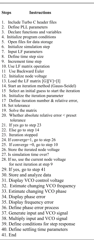
VI. THE ALGORITHM
iterated value falls below the tolerance value. The successive solutions are found by using the most recent previous value as the guess for the next iteration. The MATLAB platform is used for graphical analysis of data obtained from various simulation responses.
VII. RESULTS AND DISCUSSION
Fig.4, Fig.5 and Fig.6 show the simulation responses of VCO control voltage, VCO output frequency and frequency error at loop BW = 9 KHz for
Fig.3.The algorithm
Fig.3: The algorithm
20 MHz, 40MHz, 60MHz, 80MHz and 100MHz hop distances. Similar experiments have been performed for 18 KHz, 30 KHz, 40 KHz, 64 KHz & 91 KHz loop BW with different loop parameters and the results are given in Table
1 and Table 2.
Table 1 shows the measurement of VCO control voltage required for generating the carrier frequencies and Table 2 shows the accuracies of the corresponding carrier frequencies generated by the VCO control voltages. The responses are analyzed at 50µS.
Fig.4: VCO control voltages at loop BW= 9 KHz
[image:3.595.311.546.133.297.2]Fig.5: VCO output frequency at loop BW= 9 KHz
Fig.6: Frequency error at loop BW= 9 KHz
It is observed from Table 1 and Table 2 that for 20 MHz hopping distance at 9 KHz loop BW, the VCO control voltage error and frequency error are 1.4% at 50µS time point. If the loop BW is gradually increased up to 91 KHz, the errors reduce to 0.2% for the same 20 MHz hop distance at 50µS time point. Again, for 100 MHz hop distance with 9 Steps Instructions
1. Include Turbo C header files 2. Define PLL parameters
3. Declare functions and variables 4. Initialize program conditions 5. Open files for data storage 6. Initialize simulation step 7. Input LF parameters 8. Define time step size 9. Increment time step 10. Use LF matrix operation 11 Use Backward Euler 12. Initialize node voltage 13. Load the LF matrix [G][V]=[I] 14. Start an iteration method (Gauss-Seidel) 15 Select an initial guess to start the iteration 16. Initialize the iteration parameter
17 Define iteration number & relative error, 18. Set tolerance
19. Solve the matrix
20. Whether absolute relative error < preset tolerance
21. If yes go to step 23 22. Else go to step 14 23. Iteration stopped
24. If converge=1, go to step 26 25. If converge =0, go to step 10 26. Store the iterated node voltage 27. Is simulation time over?
28. If no, use the current node voltage for next iteration at step 9
29. If yes, go to step 41 30. Store and analyze data 31. Display VCO control voltage
32. Estimate changing VCO frequency 33. Estimate changing VCO phase 34. Display phase error
[image:3.595.65.265.194.701.2] [image:3.595.292.549.295.683.2]KHz loop BW, the error is 7.3% at 50µS time point. As the loop BW gradually increased to 91 KHz, error reduces to 0.7% for the same hop distance. Similar responses are observed for hop distance of 40, 60 and 80 MHz with different values of loop BW. It is observed that the increase of loop BW by almost ten times has resulted in the reduction of error by almost ten times. So the increased loop BW resulted faster settling time for the model, which verifies that settling time is inversely proportional to the loop BW [9].
The settling time observed in the present APLL model with a base frequency of 2.402 GHz is comparable with the results of earlier works. It is observed that the settling time around 60µS for 100 MHz hopping distance from 5.34 GHz to 5.44 GHz at loop BW of 40 KHz [9] is comparable with the results of the present work with settling time < 50µS at a loop BW of 91 KHz for hopping a distance of 100 MHz.
TABLE 1
MEASUREMENT OF ERROR IN VCO CONTROL VOLTAGE
PLL gain paramet er Kv=1G
Hz/volt Kd =0.5
v/rad Hop distance in MHz (base carrier =2.402 GHz )
Control voltage error Theore tical values (in volt) Simul ated value at 50µs (in volt) Error in % BW=9 KHz
20 0.02 0.01972 1.4 40 0.04 0.0388 3.0
60 0.06 0.0574 4.3 80 0.08 0.0754 5.7 100 0.10 0.0927 7.3 BW=18
KHz
20 0.02 0.0198 1.0 40 0.04 0.0391 2.2 60 0.06 0.0581 3.1 80 0.08 0.0766 4.2 100 0.10 0.0947 5.3
BW=30 KHz
20 0.02 0.01993 0.3 40 0.04 0.03967 0.8 60 0.06 0.05915 1.4 80 0.08 0.07849 1.8 100 0.1 0.0976 2.4 BW=40
KHz
20 .02 0.0199 0.5 40 0.04 0.0397 0.7 60 0.06 0.0594 1.0 80 0.08 0.0789 1.3 100 0.1 0.0983 1.7 BW=64
KHz
20 0.02 0.01997 0.2 40 0.04 0.0398 0.5 60 0.06 0.0596 .60 80 0.08 0.0793 .87 100 0.1 0.0989 1.1 BW=91
KHz
20 0.02 0.01996 0.2 40 0.04 0.0398 0.5 60 0.06 0.0597 0.5 80 0.08 0.0795 0.6 100 0.1 0.0992 0.8
TABLE 2
MEASUREMENT OF ERROR IN CARRIER FREQUENCY
PLL gain Parameters Kv=1GHz/
volt Kd =0.5
v/rad Hop distance in MHz ( base carrier = 2.402 GHz) Carrier frequency error Simulated value at 50µS (in MHz) Error in % BW=9 KHz
20 0.275 1.37
40 1.1 2.75
60 2.53 4.2
80 4.5 5.0
100 7.0 7.0
BW=18 KHz
20 194 0.97
40 817 2.0
60 1.8 3.0
80 3.3 4.1
100 5.2 5.2
BW=30 KHz
20 0.075 0.375
40 0.338 0.97
60 0.854 1.4
80 1.5 1.8
100 2.39 2.39
BW=40 KHz
20 0.059 0.29
40 0.259 0.64
60 0.572 0.95
80 1.04 1.3
100 1.64 1.6
BW=64 KHz
20 0.038 0.19
40 0.159 0.39
60 0.359 0.59
80 0.660 0.82
100 1.02 1.02
BW=91 KHz
20 0.034 0.2
40 0.111 0.27
60 0.220 0.36
80 0.459 0.57
100 0.721 0.72
VIII. CONCLUSION
This paper presents a simulation technique of an APLL for FHSS based application such as Bluetooth in time domain. The technique is used to generate frequency hopping carriers at 2.40 GHz ISM band to study the feasibility of the work. The hopping carrier frequencies are generated starting from 2.422 GHz to 2.502 GHz at base carrier frequency of 2.402 GHz covering hopping frequency distance from 20MHz to 100MHz. The settling times for the hopping distances are simulated observed with increasing values of loop BW and its corresponding loop parameters. The simulated responses have confirmed that the settling time is inversely proportional to the loop BW. The measured settling time is less than 50µS with around 1% error for the maximum hopping distance of 100 MHz.
values, PLL gain parameters and signal parameters like frequencies and phases. The method has the added advantage of post processing the simulated data for various other PLL related studies. The time domain aspect of the simulator helps in observing the actual behavior of signals at desired time intervals. The model has successfully simulated for settling time parameter and carrier frequency generation. The model may be suitable for frequency hopping in FHSS based application.
ACKNOWLEDGEMENT
The authors would like to thank the Head, Department of Electronics & Communication Technology (ECT), Gauhati University, Guwahati for encouragement towards the present work. One of the authors, N. Haque would like to thank the Head, Department of Electronics & Communication Engineering, Indian Institute of Technology, Guwahati for providing its excellent library facilities towards literature survey for the work.
REFERENCES
[1] Floyd M. Gardner, Phase-lock Techniques. John Wiley &Sons, 1979
[2] John L. Stesnby, Phase-Locked Loops: Theory and Applications, CRC Press, 1997
[3] Jack Smith, Modern Communication Circuits, Tata McGraw-Hill Edition, 2003
[4] N. Margaris, Theory of nonlinear behavior of the analog Phase-Locked Loop, Springer, 2003
[5] G. Hsieh and J. C. Hung, Phase-Locked Loop Techniques-A Survey, IEEE Transactions on Industrial Electronics, vol. 43, pp 609-615 No.6, December 1996.
[6] B.P Lathi & Zhi Ding Modern Digital and Analog Communication Systems Oxford University Press,New York, 2010
[7] Wayne Tomasi, Advanced Electronic Communication Systems, Pearson Education, Sixth Edition,2004
[8] Tzi-Dar Chiueh, Jin-Bin Yang, and Jen-Shi Wu,
Design and Implementation of a Low-Voltage Fast-Switching Mixed-Signal-Controlled Frequency Synthesizer IEEE transaction on circuits and systems –II; Analog and Digital signal processing ,vol.48,No.10,October,2001
[9] Wei-Hao Chiu, Student Member, IEEE , Yu-Hsiang Huang, and Tsung-Hsien Lin, Senior Member, IEEE,
A Dynamic Phase Error Compensation Technique for Fast-Locking Phase-Locked Loops, IEEE Journal of solid-state circuits, vol. 45, No. 6, June, 2010. [10] H.R. Swanepoel and S. Sinha, Members,ADesign of
a Frequency hopping spread spectrum Transceiver for cellular systems, 2004 IEEE, AFRICON,vol.97(3).
[11] Ron Kielkowski, Inside SPICE, McGraw-Hill, Inc, 1998
[12] Application Note, 1304-6, Loop BW and Clock Data Recovery (CDR) in Oscilloscope Measurements,
Agilent Technologies
[13] V.Rajaraman, Computer Oriented Numerical Methods, Prentice Hall of India Pvt. Ltd. 1998 [14] N.Haque, P.K.Boruah,T. Bezboruah, Simulation of
transient behavior of second order Phase-Locked Loops using phase error process in time domain,
Proceedings of International Conference on System Dynamics and Control, Manipal Institute-Aug22 of Technology (MIT), Manipal, Aug19, 2010