MASTER THESIS 31 August 2016
DESIGN AND IMPLEMENTATION OF AN FMCW
RADAR SIGNAL PROCESSING MODULE FOR
AUTOMOTIVE APPLICATIONS
Suleyman Suleymanov
Faculty of Electrical Engineering, Mathematics and Computer Science
Computer Architecture for Embedded Systems
EXAMINATION COMMITTEE Prof.dr.ir. M.J.G. Bekooij
Prof.dr.ir. G.J.M. Smit Ir. J.Scholten
Abstract
In the recent years, the radar technology, once used predominantly in the military, has started to emerge in numerous civilian applications. One of the areas that this technology appeared is the automotive industry. Nowadays, we can find various radars in modern cars that are used to assist a driver to ensure a safe drive and increase the quality of the driving experience. The future of the automotive industry promises to offer a fully autonomous car which is able to drive itself without any driver assistance. These vehicles will require powerful radar sensors that can provide precise information about the surrounding of the vehicle. These sensors will also need a computing platform that can ensure real-time processing of the received signals.
The subject of this thesis is to investigate the processing platforms for the real-time signal processing of the automotive FMCW radar developed at the NXP Semiconductors. The radar sensor is designed to be used in the self-driving vehicles.
The thesis first investigates the signal processing algorithm for the MIMO FMCW radar. It is found that the signal processing consists of the three-dimensional FFT processing. Taking into account the algorithm and the real-time requirements of the application, the processing capability of the Starburst MPSoC, 32 core real-time multiprocessor system developed at the University of Twente, has been evaluated as a base-band processor for the signal processing. It was found that the multiprocessor system is not capable to meet the real-time constraints of the application.
As an alternative processing platform, an FPGA implementation of the algorithm was proposed and implemented in the Virtex-6 FPGA. The imple-mentations uses pre-built Xilinx IP cores as hardware components to build the architecture. The architecture also includes a MicroBlaze core which is used to generate the artificial input data for the algorithm and manage the operation of hardware components through software.
The results of the implementation show that the architecture can provide reliable outputs regarding the range, velocity and bearing information. The accuracy of the results are limited by the range, velocity and angular
Contents
Abstract iii
List of Figures vii
List of Tables ix
List of Acronyms xi
1 Introduction 1
1.1 Context . . . 1
1.2 FMCW Radar Fundamentals . . . 2
1.3 Research Platform . . . 5
1.4 Problem Description . . . 6
2 FMCW Signal Processing 9 2.1 FMCW Signal Analysis . . . 9
2.2 MIMO Radar Concept . . . 15
2.2.1 MIMO Signal Model . . . 15
3 Requirements 19 3.1 Matlab Model . . . 19
3.2 Computational Analysis . . . 20
3.3 Architecture Considerations . . . 22
3.4 Signal-flow Analysis . . . 24
4 System Implementation 29 4.1 The algorithm . . . 29
4.2 The hardware components . . . 31
4.2.1 FFT Core . . . 31
4.2.2 AXI DMA Core . . . 32
4.2.3 Memory Interface Core . . . 33
4.2.4 Microblaze Core . . . 33
4.3 The architecture and operation . . . 33
5 Results and Analysis 39 5.1 Results . . . 39
5.1.1 Hardware Resource Usage . . . 39
5.1.2 Tests . . . 40
5.1.3 Performance . . . 41
5.2 Analysis . . . 43
5.2.1 Evaluation . . . 43
6 Conclusion 47 6.1 Conclusions . . . 47
List of Figures
1.1 FMCW radar block diagram . . . 4
1.2 Xilinx ML605 development board . . . 5
1.3 NXP Semiconductor’s automotive radar chip . . . 7
2.1 FMCW sawtooth signal model . . . 9
2.2 FMCW signal 2D FFT processing . . . 14
2.3 Principle of phase interferometry [1] . . . 14
2.4 TX and RX antennas of MIMO radar . . . 16
2.5 Virtual antenna array . . . 17
3.1 Range-Doppler Spectrum . . . 20
3.2 Birdseye view . . . 20
3.3 Radar scannings . . . 24
3.4 Signal Flow Graph of 3D FFT Procesing . . . 25
4.1 Signal processing algorithm flowchart . . . 31
4.2 The architecture of the implementation . . . 34
4.3 An example transpose operation . . . 35
5.1 Processes and their performance . . . 43
List of Tables
2.1 Parameter table . . . 12
5.1 Resource usage of the architecture . . . 40
5.2 Radar test results . . . 41
5.3 Timing results of the implementation . . . 42
List of Acronyms
ADC Analog to Digital Converter
AXI Advanced eXtensible Interface
CAES Computer Architecture for Embedded Systems
CLB Configurable Logic Block
CPU Central Processing Unit
CW Continuous Wave
DDR Double Data Rate
DFT Discrete Fourier Transform
DMA Direct Memory Access
DSP Digital Signal Processing
DVI Digital Visual Interface
FFT Fast Fourier Transform
FIFO First-In First-Out
FMCW Frequency Modulated Continuous Wave
FPU Floating Point Unit
FPGA Field-Programmable Gate Array
LMB Local Memory Bus
MIMO Multiple Input Multiple Output
MPSoC Multiprocessor System-on-Chip
NoC Network on Chip
RF Radio Frequency
SDRAM Synchronous Dynamic Random-Access Memory
SODIMM Small Outline Dual In-line Memory Module
TDM Time-Division Multiplexing
UART Universal Asynchronous Receiver/Transmitter
Chapter 1
Introduction
1.1
Context
For a long time radars have been used in multiple military and commercial applications. The development of the ideas that lead to the radar systems emerged in the late nineteenth and early twentieth centuries. However, the main developments of the system have been seen during the Second World War. During that period radars were extensively used for air defence pur-poses such as long-range air surveillance and short-range detection of low altitude targets. In the post-war period, improvements had been made in the development of the radar technology for both the military and civilian applications. Major civilian applications of the radar that emerged during that period were the weather radar and the air-traffic control radar that used to ensure the safety of the air traffic in the airports [2].
Recently, applications of radars in the automotive industry have started to emerge. High-end automobiles already have radars that provide parking assistance and lane departure warning to the driver [3]. Currently, there is a growing interest in the self-driving cars and some people consider it to be the main driving force of the automotive industry in the coming years. With the start of the Google’s self-driving car project, the progress in this area has got a new acceleration.
Self-driving cars offer a totally new perspective on the application of the radar technology in the automobiles. Instead of only assisting the driver, the new automotive radars should be capable of taking an active role in the control of the vehicle. As a matter of fact, they will be a key sensor of the autonomous control system of a car.
Radar is preferred over the other alternatives such as sonar or lidar as it is less affected by the weather conditions and can be made very small to
decrease the effect of the deployed sensor to the vehicle’s aerodynamics and appearance. The Frequency Modulated Continuous Wave (FMCW) radar is a type of radar that offers more advantages compared to the others. It ensures the range and velocity information of the surrounded objects to be detected simultaneously. This information is very crucial for the control system of the self-driving vehicle to provide a safe and collision-free cruise control.
A radar system installed in a car should be able to provide the neces-sary information to the control system in real-time. It requires to have a base-band processing system which is capable of providing enough comput-ing power to meet the real-time system requirements. The processcomput-ing system performs digital signal processing on the received signal to extract the use-ful information such as range and velocity of the surrounded objects. One of the platforms that can achieve this task is a multiprocessor system-on-chip (MPSoC) which uses multiple processors to increase the computational power.
The Starburst multiprocessor system has been developed at the Com-puter Architecture for Embedded Systems (CAES) group of the University of Twente. This system is used to carry out research on real-time design and analysis. It is prototyped on a Xilinx ML605 development board which hosts a Virtex-6 FPGA and several peripheral devices such as DDR3 SDRAM, Ethernet and UART interface. The main processing element of the Star-bust is Xilinx’s soft processor core - MicroBlaze. A number of MicroBlaze cores are connected through Network-on-Chip (NoC) with a ring topology which provides arbitration for all the processing elements connected to it. The platform also supports hardware accelerator integration to improve it’s computing capabilities [4].
The aim of this thesis is to analyze the Starburst platform from the per-spective of the requirements of the FMCW radar signal processing and pro-pose an alternative architecture if it fails to meet the real-time requirements. First, a theoretical study on the MIMO FMCW radar signal processing will be performed, second, computational requirements of the algorithm will be analyzed and based on the requirements a platform for the implementation will be chosen, third, a signal processing architecture will be designed and implemented, finally, the tests will be performed and the results will be an-alyzed.
1.2
FMCW Radar Fundamentals
1.2. FMCW RADAR FUNDAMENTALS 3 of the FMCW radar is discussed and some application examples are given.
Radar which stands for Radio Detection and Ranging, is a system that uses electromagnetic waves to detect and locate objects. A typical radar system consists of a transmitter, receiver and a signal processing module. Initially, the transmitter antenna radiates electromagnetic energy in space. If there is an object within the range of the antenna, it will intercept some of the radiated energy and reflect it in multiple directions. Some of the reflected electromagnetic waves will be returned and received by the receiver antenna. After amplification and some signal processing operations, target information such as distance, velocity and direction can be acquired [2].
Nowadays, radars are used for many different purposes. The applications of radars include but are not limited to surveillance, object detection and tracking, area imaging and weather observation. Each type of radar requires the radar sensor to have specific features which can deliver useful information to the user [2]. In case of automotive radars, the radar sensor should provide the range and the relative velocity information of the surrounded objects to the driver with a high accuracy and resolution. In addition, the sensor is desirable to be smaller in size and lower in cost. Currently, FMCW radar is the most common radar type used for this purpose [5].
FMCW radar is a type of Continuous Wave (CW) radars in which fre-quency modulation is used. The first practical application of this type of radar emerged in 1928, when it was patented by J.O.Bentley to be used on airplane altitude indicating system. Industrial applications of this radar started to appear at the end of the 1930s, after exploitation of the ultra-high frequency band. In the following years, FMCW radar had been applied in the number of civilian and military applications in which estimation of the range with a very high accuracy was crucial. Few examples of these systems are vehicle collision avoidance systems, radio altimeters and the systems to mea-sure the small motion changes caused by vibrations of various components of machines and mechanisms [6].
The theory of operation of FMCW radar is simple. FMCW radar sends a continuous wave with an increasing frequency. A transmitted wave after being reflected by an object is received by a receiver. Transmitted and re-ceived signals are mixed (multiplied) to generate the signal to be processed by a signal processing unit. The multiplication process will generate two sig-nals; one with a phase equal to the difference of the multiplied signals, and the other one with a phase equal to the sum of the phases. The sum signal will be filtered out and the difference signal will be processed by the signal processing unit [7]. The block diagram of the radar sensor can be seen in the Figure 1.1.
radars. These are [6]:
• Ability to measure small ranges with high accuracy
• Ability to measure simultaneously the target range and its relative velocity
• Signal processing is performed at relatively low frequency ranges, con-siderably simplifying the realization of the processing circuit
• Functions well in many types of weather and atmospheric conditions as rain, snow, humidity, fog and dusty conditions
• FMCW modulation is compatible with solid-state transmitters, and moreover represents the best use of output power available from these devices
• Small weight and small energy consumption due to absence of high circuit voltages
[image:16.595.171.462.444.538.2]The FMCW radar signal processing requires Fast Fourier Transform (FFT) algorithm to be implemented. More detailed coverage of this topic will be presented in Chapter 2.
1.3. RESEARCH PLATFORM 5
1.3
Research Platform
This section introduces the Starburst MPSoC and the hardware platform on which the radar application will be implemented.
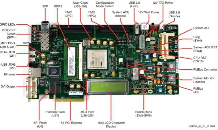
[image:17.595.101.454.321.532.2]The hardware platform ton which the application will be implemented is Xilinx’s ML605 development board (Figure 1.2). The board is equipped with a Virtex-6 FPGA which contains 241,152 logic cells, 37,680 configurable logic blocks (CLBs) and 416 36 Kb block RAM (BRAM) blocks. Additionally, the board contains several peripherals such as 512 MB DDR3 SODIMM SDRAM, an 8-lane PCI Express interface, a tri-mode Ethernet PHY, general purpose I/O, DVI output and a UART interface [8]. Currently, the platform is used for the development and testing of the Starburst MPSoC.
Figure 1.2: Xilinx ML605 development board
The Starburst MPSoC consists of number of processing tiles connected through Network on Chip. Currently, the platform supports up to 32 pro-cessing cores and a Linux core to provide an easy interaction with a host PC. In addition, the platform also supports hardware accelerator integration.
has a local memory and a scratchpad memory which sizes are reconfigurable at design time. Both memories are connected to MicroBlaze through Local Memory Bus (LMB), and can be accessed from local MicroBlaze core, al-though, the scratchpad memory is also connected to the ring interconnect and can accept data from it. All the processors run a real-time POSIX com-patible micro-kernel called Helix which supports the newlib C library and implements the Pthread standard.
The communication network of Starburst consists of two parts. The first one is the Nebula ring interconnect which supports all to all communication between processing tiles and hardware accelerators. The ring is unidirec-tional and has an arbitration policy based on ring slotting which prevents the occurrence of starvation. Each processing tile is connected to a router via a Network Interface and each router is connected to its two neighbouring routers which makes a ring-like structure. The processors are processing the stream of data and can transfer their computation results to other processors connected to the ring. The communication between processors is achieved through C-FIFO algorithm which allows arbitrary number of simultaneous streams between processor tiles. The second communication network is the Warpfield arbitration tree which provides a communication to the shared resources such as UART, DVI and SDRAM. The access to the resources is given on a first-come-first-served basis.
The Starburst MPSoC allows a number of CPUs to run in parallel to achieve a high computation power. Additional support of hardware accel-erators allows to improve the performance for the applications which are limited by the computational power of MicroBlaze cores. The resulting het-erogeneous MPSoC is an important research and development platform for the stream processing applications which also allows real-time multiprocessor system analysis [4].
1.4
Problem Description
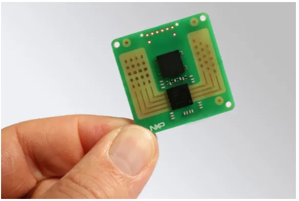
Recent developments in the digital electronics has led to the major improve-ments in number of areas. Novel microwave transmitters are capable of generating extremely high frequency signals in real time which allows the usage of these high frequency signals in numerous applications. Recently, number of automotive radar chips have emerged which take advantage of the mm-Wave band such as 77 Ghz and 79 Ghz [3].
self-1.4. PROBLEM DESCRIPTION 7 driving vehicles such as self-driving cars. Currently, researchers at NXP Semiconductors are working on the development of the base-band processor for the above mentioned chip.
Figure 1.3: NXP Semiconductor’s automotive radar chip
This thesis works as a supportive research to test concepts of the Starburst MPSoC to be used in a base-band processor. The main aim of this research is to analyse the computational and real-time requirements of the FMCW radar application and extend the Starbust MPSoC platform accordingly to support the MIMO FMCW radar signal processing.
The main research objectives for the thesis are:
• Research the theory of the MIMO FMCW radar signal processing and evaluate the proposed signal processing architectures.
• Propose the efficient architecture for the Starburst platform to support the FMCW radar application.
Chapter 2
FMCW Signal Processing
This section consists of two main parts; the first part explains the FMCW signal processing scheme and the second part introduces the MIMO radar concept.
2.1
FMCW Signal Analysis
[image:21.595.85.461.484.630.2]There are several different modulations that are used in FMCW signals such as sawtooth, triangle and sinusoidal. In our case, we will consider a sawtooth model of the FMCW signal, seen in the Figure 2.1;
Figure 2.1: FMCW sawtooth signal model
As it can be seen, transmitted frequency increases linearly as a function of time during Sweep Repetition Period or Sweep Time (T). Starting frequency isfc, which is 79 GHz in our calculations. Frequency at any given time t can
be found by:
f(t) = fc+
B
Tt (2.1)
Here, BT is a chirp rate and can be thought as a “speed” of the frequency change. We can substitute it with α:
α= B
T (2.2)
By using frequency change over time, we can find the instantaneous phase:
µ(t) = 2π
Z t
0
f(t)dt+µ0 = 2π(fct+
αt2
2 ) +ϕ0 (2.3)
Therefore, the transmitted signal in the first sweep, consideringϕ0 to be the
initial phase of the signal, can be written as:
xtx(t) = Acos(µ(t)) =Acos(2π(fct+
αt2
2 ) +ϕ0) (2.4)
The equation above only describes the transmitted signal in the first sweep. If we want to describe the transmitted signal in thenthsweep, a modification
should be made. We can consider ts as a time from the start of nth sweep
and define t as:
t=nT +ts where 0< ts < T (2.5)
Therefore, our signal form for the transmitted signal in the nth sweep
be-comes:
xtx(t) =Acos(µ(t)) =Acos(2π(fc(nT +ts) +
αt2s
2 ) +ϕ0) (2.6)
Let’s consider an object located at an initial distance of R which is moving with a relative velocity of v. The returned signal from the object will have the same form, but with some delayτ which can be defined as:
τ = 2(R+vt)
c =
2(R+v(nT +ts))
c (2.7)
Considering the delayτ, we can describe the returned signal as:
xrx(t) =Bcos(µ(t−τ)) =Bcos(2π(fc(nT+ts−τ)+
α(ts−τ)2
2 )+ϕ0) (2.8)
According to the FMCW radar principle, the returned signal is mixed with the transmitted signal:
2.1. FMCW SIGNAL ANALYSIS 11 The equation above will include cosine multiplication which can be trans-formed using the trigonometric formula below:
cos(α) cos(β) = (cos(α+β) + cos(α−β))/2 (2.10)
The sum term in our case will have a very high frequency (2·fc= 158GHz)
which will be filtered out. Therefore, the resulting signal will only include the subtraction term:
xm(t) =
AB
2 cos(2π(fc(nT+ts) +
αt2
s
2 −fc(nT+ts−τ)−
α(ts−τ)2
2 ) (2.11)
After simplification we get:
xm(t) =
AB
2 cos(2π(fcτ+ατ ts−
ατ2
2 )) (2.12)
If we replace τ with its equivalent from Equation 2.7, we will get:
xm(t) =
AB
2 cos(2π(fc
2(R+v(nT +ts))
c +αts
2(R+v(nT +ts))
c
−α4(R+v(nT +ts)) 2
2c2 ))
(2.13)
We can simplify and write the equation as:
xm(t) =
AB
2 cos(2π(( 2αR
c +
2fcv
c +
2αvnT
c −
4αRv
c2 −
4αnT v2 c2 )ts
+(2fcv
c −
4αRv
c2 )nT +
2fcR
c +
2αvt2
s
c −
2αR2 c2
−2αv
2n2T2
c2 −
2αv2t2s c2 ))
(2.14)
If we look at the Equation 2.14, we see that there is a frequency and a phase that influences how the signal changes over time. In the literature, the frequency is usually named as a ”beat frequency”. The difference in frequency between the transmitted and the received signals is denoted by
fB in the Figure 2.1. The above equation shows that the ”beat frequency”
is affected by number of terms such as initial range to the object, object’s velocity and the chirp number.
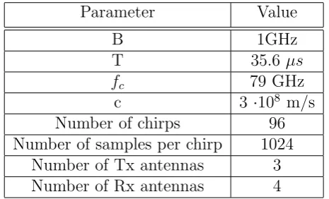
Parameter Value
B 1GHz
T 35.6 µs
fc 79 GHz
c 3 ·108 m/s
Number of chirps 96
Number of samples per chirp 1024
Number of Tx antennas 3
[image:24.595.202.435.125.266.2]Number of Rx antennas 4
Table 2.1: Parameter table
If we assume an object at a distance of 15 m (R = 15) which is moving with a velocity of 10 m/s (v = 10), and assuming ts equal to T andn to be
50, we can find how the individual expressions in the equation affect the final value ofxm(t):
xm(t) =
AB
2 cos(2π((2.81·10
6+ 5.26·103+ 3.33·103−0.1873
−2.22·10−4)ts+ (5260−0.19)nT + 7.9·103
+0.0024−0.1404−1.97·10−7−7.9·10−11))
(2.15)
Few observations can be made based on the equation above; first, we see that the values of the expressions 4αRvc2 and
4αnT v2
c2 are very small and can
easily be neglected. Apart from that, the terms 2fcv
c and
2αvnT
c are relatively
small and their effect to the main frequency component 2αRc can be considered negligible. Second, other terms which havec2 in their denominators are also very small and can be neglected too. Third, the term with t2
s,
2αvt2
s
c is also
very small (0.0024) and can be neglected as well.
Consequently, xm(t) equation can be approximated as:
xm(ts, n) =
AB
2 cos(2π( 2αR
c ts+
2fcvn
c T) +
4πfcR
c ) (2.16)
where the term 4πfcR
c is a constant phase term, since R is an initial distance
at which the object is located.
2.1. FMCW SIGNAL ANALYSIS 13 frequency (2.17) and thus the range to the target:
fb =
2αR
c and R=
fbc
2α (2.17)
Range resolution of a radar is the minimum range that the radar can distinguish two targets on the same bearing [9]. Based on the above equation and substituting α with Equation 2.2, we can find the range resolution of a radar. It is based on the fact that the frequency resolution ∆fb of the mixed
signal is bounded by the chirp frequency (∆fb ≥ T1) which means that in
order to be able to detect two different objects, the frequency difference of the mixed signal returned from that objects cannot be smaller than the chirp frequency. This intuition gives the range resolution which can be found as:
∆fb =
2B∆R
c ·
1
T and ∆R =
c
2B (2.18)
On the other hand, there is also a phase (2fcv
c ·nT) associated with the beat
frequency which changes linearly with the number of sweeps. The change of the phase indicates how the frequency of the signal changes over consequent number of periods. This change is based on the Doppler frequency shift which is the shift in frequency that appears as a result of the relative motion of two objects. The Doppler shift can be used to find the velocity of the moving object:
fd=
2fcv
c and v =
fdc
2fc
(2.19)
The Doppler shift of the signal can be found by looking at the frequency spectrum of the signal over n consecutive periods (n·T). In this case, the FFT algorithm is applied on the outputs of the first FFT. Figure 2.2 describes this process; first, the row-wise FFT is taken on the time samples, second, the column-wise FFT is taken on the output of the first FFT. After two dimensional FFT processing, we have a range-Doppler map which contains range and velocity information of the target.
Velocity resolution of a radar is the minimum velocity difference between two targets travelling at the same range of which the radar can distinguish. It can be found in a similar way as the range resolution. Here, the Doppler fre-quency change overn chirp durations is bounded by the frequency resolution (∆fd≥ nT1 ). Thus, the velocity resolution can be expressed as:
∆v = c 2fc
· 1
nT (2.20)
Figure 2.2: FMCW signal 2D FFT processing
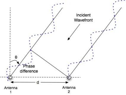
have a different phase shift based on the distance. This information can be used to find the angle of arrival of the wave and thus angular position of the target. To achieve that a third FFT can be taken over processed signals from different antennas. Using a phase comparison mono-pulse technique, see Figure 2.3, we can find the phase shift between two array antennas.
Figure 2.3: Principle of phase interferometry [1]
If antennas are located in distance d from each other, and the angle of arrival of waves isθ, we can find the phase difference through Equation 2.21, whereλ is the wavelength of the signal:
∆ϕ= 2πdsin(θ)
λ (2.21)
[image:26.595.212.425.365.526.2]2.2. MIMO RADAR CONCEPT 15 can rewrite 2.16 as:
xm(ts, n, k) =
AB
2 cos(2π( 2αR
c ·ts+
2fcvn
c ·T +
dksinθ
λ ) +
4πfcR
c ) (2.22)
where 0 ≤k ≤ K−1 and 1≤ n ≤ N, and N is the total number of chirps per frame.
2.2
MIMO Radar Concept
Multiple input multiple output (MIMO) radar is a type of radar which uses multiple TX and RX antennas to transmit and receive signals. Each trans-mitting antenna in the array independently radiates a waveform signal which is different than the signals radiated from the other antennas. The reflected signals belonging to each transmitter antenna can be easily separated in the receiver antennas since orthogonal waveforms are used in the transmission. This will allow to create a virtual array that contains information from each transmitting antenna to each receive antenna. Thus, if we have M number of transmit antennas and K number of receive antennas, we will haveM·K
independent transmit and receive antenna pairs in the virtual array by using only M +K number physical antennas. This characteristic of the MIMO radar systems results in number of advantages such as increased spatial reso-lution, increased antenna aperture, higher sensitivity to detect slowly moving objects [10, 11].
2.2.1
MIMO Signal Model
As stated above, signals transmitted from different TX antennas should be orthogonal. Orthogonality of the transmitted waveforms can be obtained by using time-division multiplexing (TDM), frequency-division multiplexing and spatial coding. In the presented case, TDM method is used which allows only a single transmitter to transmit at each time. Considering M number of transmitting antennas and K number of receiving antennas (Figure 2.4), the transmitting signal from ith antenna towards target can be defined as:
xtx(t, m) = Acos(µ(t) +
2πdtmsinθ
λ ) (2.23)
where 0≤k ≤K−1 and 0≤m≤M −1.
The corresponding received signal at jth antenna can be expressed by:
xrx(t, m, k) =Bcos(µ(t−τ) +
2πdtmsinθ
λ +
2πdrksinθ
and consequently the difference signal can be written as:
xm(ts, n, m, k) = cos(2π(
2αR c ·ts+
2fcvn
c ·T+
dtmsinθ
λ +
drksinθ
λ )) (2.25)
The steering vector represents the set of phase delays experienced by a plane wave as it reaches each element in an array of sensors. By using the equations above, we can describe the steering vector of transmitting array as:
at(θ) = [1, e
−j2πdtsinθ
λ , e
−j2πdt2 sinθ λ , ..., e
−j2πdt(M−1) sinθ
λ ]T (2.26)
and the steering vector of receiving array as:
ar(θ) = [1, e
−j2πdr sinθ
λ , e
−j2πdr2 sinθ λ , ..., e
−j2πdr(K−1) sinθ
[image:28.595.153.512.236.421.2]λ ]T (2.27)
Figure 2.4: TX and RX antennas of MIMO radar
The steering vector of the virtual array (Figure 2.5) can be found by the Kronecker product of the steering vector of transmitting array and the steering vector of receiving array. Kronecker product can be thought as multiplying each element of the first vector with all the elements of the second vector and concatenate all the multiplication results together to form one vector. Kronecker product of two vectors sized M ×1 and K×1, will result in an M ×[K ×1] size vector. Thus, steering vector of the virtual array can be expressed by:
av(θ) =at(θ)⊗ar(θ) = [1, e
−j2πdr sinθ λ , ..., e
−j2πdtsinθ
λ , e
−j2π(dt+dr) sinθ
λ ,
..., e−j2π(dt(M−1)+λdr(K−1)) sinθ]T
(2.28)
The vector above contains phase delays that waveform experiences in its path from each transmitting antenna to each receiving antenna. It can be used to find the angular position of the object which can be expressed as:
P(θ) =
L−1
X
l=0
Xl(f)·alv(θ) = M−1
X
m=0
K−1
X
k=0
Xm,n(f)·e
−j2π(dtm+dr k) sinθ
2.2. MIMO RADAR CONCEPT 17 where L is the number of elements in the virtual array and Xl(f) refers to
the spectrum of the signal in thelth virtual array element andal
v(θ) refers to
[image:29.595.149.397.243.328.2]thelthelement of the steering vector. Intuitively, the formula above finds the amplitudes (gains) associated with the angle of arrivals (AOA) in the whole imaging area. It can be thought as finding a frequency spectrum of a time-domain signal where frequency corresponds to direction and time samples correspond to space samples:
Figure 2.5: Virtual antenna array
Consequently, assuming antennas in the virtual array uniformly spaced and distance between two antennas is d, we can find the relation between θ
and virtual array as:
L−1
X
l=0
Xl(f)·e
−j2πsl
L =
L−1
X
l=0
Xl(f)·e
−j2πdlsinθ
λ (2.30)
where the range of s is 1≤s≤L.
The left side of the Equation 2.30 is the Discrete Fourier Transform and the right side is the Equation 2.29 modified for virtual array representation. The equation above will help us to describe the relation of a virtual antenna number or FFT bin s with AOA (θ):
− j2πsl
L =−
j2πdlsinθ
λ (2.31)
which gives us θ expressed as:
θ = arcsinsλ
dL (2.32)
Chapter 3
Requirements
This chapter describes the analysis of the algorithm that the signal processing is based on. The first section describes the Matlab model of the radar signal processing. The second section provides the computational analysis on the FFT algorithm which is the main functional block of the signal processing and gives the requirements for the architecture to be implemented. The next section discusses the architectures proposed in the recent literature. Finally, the last section provides a signal-flow analysis of the radar processing.
3.1
Matlab Model
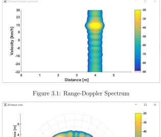
The Matlab model of the reception part of the radar application was provided by the NXP Semiconductors. The essential part of the code is 3D FFT mod-ule which is used to get the frequency domain representation of the received signals from their time and space domain equivalents. Later, the frequency domain representation is used to plot the Range-Doppler spectrum and the bearing information. Provided code had no measurement file that could be used to test the model. To be able to test the radar Matlab function was implemented which generates an input signal based on the MIMO FMCW model presented in Chapter 2. The function implements the Equation 2.25 from Chapter 2 with three transmitting and four receiving antennas. The output of the tested Matlab model can be seen in the Figure 3.1 and 3.2. The input signal was generated considering an object located at 4 m initial distance with 1 rad counter-clockwise angular position and moving with a relative velocity of 4 m/s (14.4 km/h). Figure 3.1 shows the range-Doppler spectrum of the radar. It can be seen that the range of the the target is 4 m and its relative velocity is around 15 km/h. Figure 3.2 shows the relative position of the object with respect to the radar transceiver.
Figure 3.1: Range-Doppler Spectrum
Figure 3.2: Birdseye view
3.2
Computational Analysis
We have seen in Chapter 2 that the main processing block of the radar application is the FFT block. The FFT is a fast algorithm that computes the discrete Fourier transform of the time domain samples xn:
Xk= N−1
X
n=0 xne−
2πi
N nk (3.1)
The algorithm allows to reduce the complexity of the DFT computation from
O(n2) to O(nlogn).
3.2. COMPUTATIONAL ANALYSIS 21 The platform has enough processing cores to support simultaneous process-ing of signals comprocess-ing from multiple receivprocess-ing antennas. Hence, it should be studied if MicroBlaze cores could provide enough computing power for the FFT processes used in the signal processing while taking into account the real-time constraints of the application.
The computational requirements for the FFT process can provide us with an overview of the required computational power. The analysis of the al-gorithm shows that N point FFT requires N2(log2N) number of complex multiplications and Nlog2N number of complex additions. Taking into ac-count the fact that multiplications in the last stage of the FFT are simply multiplications by 1, we can exclude the multiplication operations in that stage. Therefore, the number of complex multiplications required will be
N
2(log2N −1). Additionally, each complex multiplication contains four real
multiplications and two real additions. By combining these two we can ex-press the number of real multiplications (RM) required as:
RM = 2N(log2N −1) (3.2)
Similarly, each complex addition contains two real additions. As a result, the number of real additions (RA) can be expressed as:
RA=N(log2N−1) + 2Nlog2N (3.3)
According to the MicroBlaze Reference Guide, the core has a Floating Point Unit (FPU) which supports single-precision floating point arithmetic. As stated in the reference, floating-point addition and multiplication requires 4 clock cycles in non-area optimized mode and 6 clock cycles in area optimized mode. Considering using the single-precision floating point numbers and configuring the MicroBlaze core in non-area optimized mode, we can find the number of clock cycles (NCC) required for the FFT processing as:
N CC = 4·(RM +RA) (3.4)
for the computation since it only takes into account the actual computation required by the FFT algorithm and excludes the overheads such as variable initializations, function calls, loops and memory accesses. It can be concluded that the result is 54 times larger than the provided chirp time which is 35.6
µs. Consequently, we can conclude that it is not possible to meet the real time requirements by using one MicroBlaze core as an FFT processor.
The calculations show that even if we are able to use fixed-point arith-metic for the FFT process, we are not able to reach the real-time requirement needed. The MicroBlaze reference guide [13] specifies that the integer addi-tion and multiplicaaddi-tion take 1 clock cycle to finish. By following the same procedure as above, we can calculate and find that the fixed-point FFT pro-cess will take at least 48128 clock cycles (481.28 µs) to finish which is 13.5 times bigger than the requirement.
The analysis above shows that using only the Microblaze processors in the Starburst architecture for base-band processing will not allow to achieve the real-time requirements demanded by the application. Although, the Star-bust platform also supports a hardware accelerator integration, the current application does not benefit from it. Therefore, we should consider alterna-tive architectures that can provide better performance characteristics. In the next section we discuss the architecture considerations that can lead to the higher performance.
3.3
Architecture Considerations
We have seen in Chapter 2 that the three dimensional FFT processing can give us the range, velocity and the relative position information of the target. In the previous section, we discussed the computational requirements of the FFT and found out that using MicroBlaze soft cores for FFT processing does not allow us to meet the real-time requirements. Consequently, we concluded that the Starbust architecture is not very useful in terms of meeting the real-time demands of the radar application. This section discusses the architecture that can be used to achieve the real-time performance in the Virtex-6 FPGA.
3.3. ARCHITECTURE CONSIDERATIONS 23 written to the second SDRAM while the processed data from the first frame is read from the first SDRAM for the second FFT processing. However, the authors provide no details about the resource usage and the performance of the proposed implementation.
In [15], the authors propose an architecture for range-Doppler processing which supports sampling rates up to 250 MSPS and a maximum of 16 parallel receiving channels. The architecture uses digital down-sampling to enable various sampling frequencies to be used and a low pass FIR filter to suppress the aliasing effects arising from the down-sampling process. Similar to [14], the data after the first FFT processing is stored in the SDRAM. The authors propose to interleave the usage of multiple banks of the SDRAM to improve the data throughput. That is, the outputs of the first FFT block should be distributed over multiple banks. The paper describes an example addressing scheme based on that idea which reduces processor stall cycles. In spite of the fact that the detailed resource usage of the implementation on Virtex-7 FPGA is given, no information on the performance is provided in the paper. The architecture described in [16] allows a pipelined and parallel hard-ware implementation of signal processing for an FMCW multichannel radar. The architecture supports a 3D FFT based signal processing algorithm which has been described in Chapter 2. It consists of the FFT processing blocks for range, Doppler and beamforming calculations and the dual-port memory blocks inserted between them to store the intermediate data. In contrast to the architectures described above, this implementation does not use the SDRAM and takes advantage of the FPGA on-chip memory blocks instead. In addition, the authors provide the hardware resource usage of the archi-tecture and the processing time of the algorithm implemented on Virtex-5 FPGA.
Another architecture for the radar signal processing is described in [17]. The RF front end of the design has four transmit and four receive antennas and applies the TDM technique for the transmit signals. This allows sixteen virtual antennas to be synthesized. Consequently, the processing of the re-ceived signal is based on the MIMO virtual array concept. The architecture uses an 1D FFT processing to extract the range information from the ”beat” signal and a digital beamformer to find the angular information. The imple-mentation of the architecture is based on combined FPGA and DSP pipeline approach. The FFT processing is done on the FPGA side, on the other hand the beamforming algorithm runs on the DSP side. After the processing, the radar image is displayed on the LCD panel which is actuated by the FPGA at a frame rate of 50 Hz. According to the authors, the implementation can achieve a real-time imaging rate of 1.5625 Hz.
types of architectures for the hardware implementation of the algorithm. The first type uses the off-chip SDRAM to store the intermediate results of the processing. The architectures presented in [14] and [15] are based on this type. In this type it is important to minimize the time required to open and close a page of the SDRAM when accessing the data for the second and the third FFT processings. The second type of architecture uses on-chip FPGA memory blocks to store the intermediate results. This type of architecture is more efficient and can achieve faster processing due to the fact that there is much less overhead in accessing the intermediate data of on-chip FPGA memory blocks rather than the SDRAM. However, it should be noted that this architecture is limited by the amount of available on-chip memory and will bound the number of points used for the FFT processing.
3.4
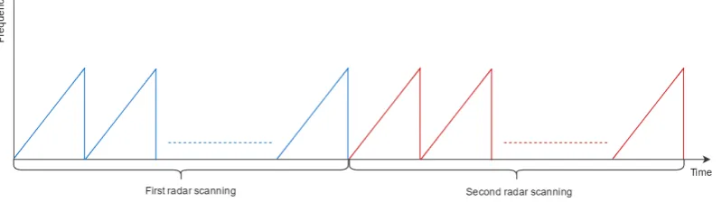
Signal-flow Analysis
[image:36.595.129.529.493.605.2]In the Matlab model described in Section 3.1, we have considered only a single radar scanning. From the provided model it is not clear if the radar will start the consecutive scanning immediately after finishing the previous scanning or there will be a time interval between them. Here we consider a model in which the consecutive scannings happen without any time interval (see Figure 3.3). Therefore, we will consider the performance of the implementation to be real-time if it provides enough computational power to process the consecutive radar scannings without any delays.
Figure 3.3: Radar scannings
3.4. SIGNAL-FLOW ANALYSIS 25 FFT is performed on 1024 time samples from one chirp period. To achieve a real-time performance, the worst case computation time of the first FFT block should be equal to the chirp time which is 35.6µsbased on our model. It means that we can process a frame as soon as it is available, thus avoiding any time delays. In addition, the outputs of the FFT block should be stored in a memory for further Doppler processing. Given the worst-case execution time (WCET) of the FFT block and the number of samples required to be stored in the memory, we can calculate the required minimum bandwidth from the first FFT block to the memory
B1 =
1024
Tc
= 1024
[image:37.595.85.468.269.422.2]35.6·10−6 = 28.76M S/s (3.5)
Figure 3.4: Signal Flow Graph of 3D FFT Procesing
The ADC used for the sampling of the received signal has 12 bits of resolution. Knowing that the output of the FFT is a complex-valued number, we can easily calculate the minimal memory required to store the FFT data. Our model uses 96 chirps per frame, thus our memory requirement equals to 96·1024·2·12 = 2359296 bits = 294912 bytes.
the total time for that processing is n·T c, where n is the number of chirps and Tc is the chirp time. Therefore, given the parameters we can find the
worst-case computation time for the second FFT:
T2 = n·Tc
1536 =
96·35.6·10−6
1536 = 2.22µs (3.6)
All the outputs from the FFT block should be stored for the third FFT processing. As it can be seen in Figure 3.4, there are three 2D arrays for the single receiving antenna each of them containing 16384 (512·32) complex values. We can easily calculate the memory required for each of the arrays which equals to 32·512·2·12 = 393216 bits = 49152 bytes.
Given WCET of the second FFT block we can find the required minimum bandwidth from block to the memory:
B2 =
32
T2 =
32
2.22·10−6 = 14.4M S/s (3.7)
The third FFT is performed on samples from all Range-Doppler spectrum’s. Considering the real-time constraints, the required time to complete all the FFTs equals to n·T c. The number of points that the third FFT performs is based on the equation provided on Matlab model:
N = 2dlog2A∗Ke (3.8)
where A is the interpolation factor for the Angle of Arrival spectrum and
K is the number of virtual antennas. Considering only a single FFT block, worst-case execution time of the block will be:
T3 =
96·35.6·10−6
16384 = 0.21µs (3.9)
Consequently, the bandwidth can be found as:
B3 =
N
0.21·10−6 (3.10)
3.4. SIGNAL-FLOW ANALYSIS 27 Based on the Figure 3.4, we can calculate that the memory requirement for a single antenna as:
M EM = 2·(294912 + 49152·3) = 884736bytes (3.11)
The application requires to have 4 receiver antennas. We can find that the memory requirement for the receiver with four antennas is around 3.5 MByte (4·884736 bytes). According to the Xilinx Virtex-6 FPGA family documentation, the Virtex6 FPGA deployed on the ML605 board XC6VLX240T -has maximum 1.872 MByte block ram capability which is considerably less than the required memory for our application. This requirement adds a con-straint of using the off-chip SDRAM to store the intermediate results of the FFT processing.
Furthermore, it should be noted that the above mentioned requirement can change based on the design decisions. To illustrate, if we consider having enough time between consecutive radar scannings and consider using an in-place computation, then the actual minimum memory requirement will be equal to 4·96·1024·2·12 = 9437184 bits = 1.125 MByte. We can see that it is considerably less than the memory available in the FPGA.
However, representing a 12 bit value with 12 bit fixed-point format will not be very reliable as it does not allow any bit growth and might result in serious errors in the calculations. Instead, a common 16 bit fixed-point format can be used for that purpose. We can find that the memory require-ment in this case will be equal to 4·96·1024·2·16 = 12582912 bits = 1.5 MByte. It is still less than the available on-chip FPGA memory and can fit in it if the other hardware components require less than 0.372 MByte of on-chip memory.
Chapter 4
System Implementation
The previous chapter presented the analysis of the algorithm and the archi-tectures found in the literature to implement it. This chapter will describe the architecture that is used to implement the algorithm on the Virtex-6 FPGA based on the given requirements. The first section describes the implemented algorithm based on the signal processing scheme described in Chapter 2 and the requirements found in Chapter 3. The second section presents the com-ponents or hardware blocks required to implement the processes found in the algorithm. Finally, the last section describes the hardware architecture that has been used to implement the algorithm.
4.1
The algorithm
This section describes the three dimensional FFT processing algorithm on which the signal processing is based on.
The first process in the algorithm is performing 1024 point FFT on the time samples. In Chapter 3 we found that the storage of the intermediate results of the FFT processing should be stored in the off-chip SDRAM. There-fore, the output of the first FFT process must be written to the SDRAM. The second FFT process will read the data from the SDRAM and perform the transform. It was mentioned in Chapter 2 that this process can be thought as a column-wise FFT of a matrix. Thus, all the 512 data samples from the 32 different chirps (rows) will be read at a different time slices. To illustrate, first the first column of data samples will be read from 32 different chirp outputs, second the second column of data samples will be read from the 32 different chirps and so on. This process will continue till all the 512 data sam-ples have been read. Knowing how the modern DRAM memories function, we observe that this is not an efficient way of addressing the SDRAM.
Modern SDRAM memories are usually organized in multiple banks. Each bank has a matrix structure and consists of rows and columns. To access a memory address for reading or writing requires to activate a row which will read the data stored in the row to the row buffer. After activating the row the data can be read or written based on the column addresses. After reading or writing the data, the row will be closed and the data will be written back to the bank. Thus, accessing the memory address requires three operations; activating the row, doing a read or write operation and closing the row. It is clear that it will introduce a huge overhead if the memory is addressed in an arbitrary order.
The ML-605 board contains 512 MB DDR3 SDRAM from Micron Tech-nology (MT4JSF6464HY-1G1B) [8]. The module has 4 chips placed on the board each having 16 bits data output. In addition, the module is organized in 8 internal device banks. Each bank has 8K rows and 1K columns. It is easy to find that each row of the bank can store 8 KByte of data. If we use single-precision floating point representation, each row of a bank will contain a processed FFT data from a single chirp, since each complex-valued number contains 8 Bytes and having 1024 numbers will make 8 KByte. Therefore, the second FFT will require to open and close a row for reading of each sam-ple which will make in total 16384 (32·512) requests per virtual antenna. This process can add significant delays to the FFT processing time.
One way to overcome this overhead is to transpose the data matrix. We can transpose the data stored in 32x1024 matrix to 1024x32 matrix form. In this way the memory addressing will be in sequential order resulting in less overhead in reading the data from the SDRAM. Thus, we need to have a memory transpose process after finishing the first FFT processing of all chirps from a given frame. After completing the transpose operation, the second FFT can be performed on the data.
4.2. THE HARDWARE COMPONENTS 31 To summarize, we have seen that the algorithm consists of multiple FFT and transpose operations. The whole process can be described with the following algorithmic flowchart.
Figure 4.1: Signal processing algorithm flowchart
4.2
The hardware components
This section describes the hardware components used in the architecture implementation. A brief description and function of all the components have been provided.
4.2.1
FFT Core
16. The core supports processing with fixed-point data ranging from 8 to 34 bits as well as single-precision floating point data. In the latter case, the input data is a vector of N complex values represented as dual 32-bit floating-point numbers with a phase factors represented as 24 or 25-bit fixed point numbers.
The FFT core provides four architecture options;
• Pipelined Streaming I/O
• Radix-4 Burst I/O
• Radix-2 Burst I/O
• Radix-2 Lite Burst I/O
The pipelined streaming architecture pipelines several Radix-2 butterfly processing engines to allow continuous data processing. Each processing engine has its own dedicated memory banks which are used to store the input and intermediate data. This allows the core to simultaneously perform a transform on the current frame of data, load input data for the next frame of data and unload the results of the previous frame of data.
For the current implementation, the pipelined streaming architecture was chosen for the two main reasons. First, the pipelining allows the FFT block to receive the data while it is processing the data from the previous frame. This is convenient for the first FFT processing in our application, since it eliminates the need for buffering of the incoming data and allows the data immediately to be received by the FFT block. Second, the processing latency of the pipelined streaming architecture is much less than the latency of the burst-architectures and meets the latency constraints found in Section 3.4.
The FFT IP core is compliant with the AXI4-Stream interface. All in-puts and outin-puts to the FFT core use the AXI4-Stream protocol. Since the FFT core needs to access to the main memory to read a data, we need an additional hardware block which can access the memory and translate the AXI4-Memory Mapped (AXI4-MM) transactions to AXI4-Stream (AXI4-S) transfers and vice versa. This is achieved by using LogiCORE IP AXI DMA core [19] of Xilinx.
4.2.2
AXI DMA Core
4.3. THE ARCHITECTURE AND OPERATION 33 Stream to Memory-Map (S2MM) channel. Reading a data from the mem-ory is accomplished by AXI4 Memmem-ory Map Read Master interface and AXI MM2S Stream Master interface. On the other hand, writing a data to the memory is achieved through AXI S2MM Stream Slave interface and AXI4 Memory Map Write Master interface. The core also has an AXI4-Lite slave interface which is used to access the registers and control the DMA engine.
The DMA core allows maximum 8 MByte of data to be transferred be-tween a memory and a stream peripheral per transaction. According to the documentation [19], the core can achieve high throughput in transfers, namely; 399.04 MByte/s in MM2S channel and 298.59 MByte/s in S2MM channel.
4.2.3
Memory Interface Core
To access an off-chip memory from an FPGA a memory controller is required. Xilinx provides a memory interface core [20] to interface the FPGA designs to DDR3 SDRAM devices. The core handles the memory requests from hard-ware blocks such as AXI DMA and translates them to SDRAM commands. It allows the data movement between FPGA user designs and the external memory. In addition, the core also manages the refresh operation of the memory.
4.2.4
Microblaze Core
The information about the Microblaze core was provided in Chapter 1. The design uses a single Microblaze core to generate the input data for the algo-rithm, to configure the AXI DMA blocks for data transfers, to transpose the memory, to measure the time required for each process and to extract the range, velocity and the angle information form the frequency spectrum data.
4.3
The architecture and operation
The hardware components of the architecture were described in the previous section. This section describes how the components are interconnected to each other and how the architecture functions.
The architecture of the implementation can be seen in the Figure 4.2. The figure shows the hardware blocks implemented in the FPGA and the communication channels between that blocks and SDRAM. The widths of the data buses between FFT block, AXI DMA block and Memory Interface Core are 64 bit. The Microblaze core and AXI-Lite channels of the AXI DMA blocks are connected to the 100 MHz clock source. The channels of the FFT cores and the other channels of the AXI DMA blocks run at 200 MHz clock frequency and the main memory runs at 400 MHz clock frequency.
[image:46.595.121.523.391.629.2]Based on the provided input data, such as range of the target, its veloc-ity and angular information, the Microblaze core generates an input data in single-precision floating-point arithmetic and stores it in the SDRAM. Fol-lowing that, the Microblaze initializes the AXI DMA block to read the data stored in the SDRAM, transfer it to the first FFT block and writes back the output data from the block. In the design, a single AXI DMA and single FFT block are used for the processing of the whole 3D array. With the cur-rent design, having multiple DMA and FFT blocks will not accelerate the processing since all the instructions of the Microblaze run sequentially.
Figure 4.2: The architecture of the implementation
4.3. THE ARCHITECTURE AND OPERATION 35 the Microblaze core by doing the column-wise reads from the SDRAM and row-wise writes to the SDRAM. The output of this operation is a matrix in 12x512x32 3D format. Following that, the Microblaze will instruct the second AXI DMA block to start fetching the data from the SDRAM, transfer it to the second FFT block and write back the results from it. After completion of the second FFT operation, the Microblaze will transpose the data for the last FFT processing. The output of this transpose operation will have 512x32x12 3D matrix format where the third dimension contains the data from all virtual antennas. The Microblaze now can instruct the DMA block to transfer the data for the third FFT process. Although we have 12 data samples available, based on the Equation 3.8 in Chapter 3, 32 point FFT will be performed on the data. This means that the fetched data vector will be padded with zeros before processing. Consequently, the third FFT process can use the same hardware blocks used in the second FFT since they both need the same number of point FFT core. In a similar way, the output of the third FFT will be stored in the SDRAM.
Figure 4.3: An example transpose operation
angle equations derived in Chapter 2.
The range of a target and it’s velocity are found as following; first, 2D FFT processed signal data from the first virtual antenna is taken and it’s absolute value is calculated, then, a maximum value in the 2D matrix and it’s location were found, following that, based on the row (range bin -rb) and
column (velocity bin - vb) location information, the range and the velocity
of the target were calculated. Based on the Equation 2.17 in Chapter 2, the range can be found as:
R = fbc 2α =
rbfsc
2αN (4.1)
wherefs is the sampling frequency of the mixed signal and equals to:
fs =N/T (4.2)
In a similar way, based on the Equation 2.19 in Chapter 2, the velocity of the target can be found as:
v = fdc 2fc
= vbfchc 2fcn
(4.3)
wherefch is the chirp frequency and equals to:
fch= 1/T (4.4)
The angle information is found as following; first, data samples were taken from all virtual antennas based on the row and column information from the previous calculation making a snapshot vector, second, absolute values of the vector elements were calculated and stored in a vector, following that, angle bin values were calculated using the Equation 2.32 in Chapter 2, finally, based on the bin location of the maximum value of the vector, the angle value is found. The distance between virtual antenna elements was taken to be equal to the distance between receiving antennas. It should be noted that the first half of the snapshot vector represents the positive angles which range between 0o and 90o, while the second half of the vector will contain
the magnitude of the angle bin values in -90o - 0o range. Consequently, by combining them together we will have a bird’s-eye view in -90o - 90o range.
4.3. THE ARCHITECTURE AND OPERATION 37 the time required to finish these FFT processes will be 21.185 µs and 1.14
Chapter 5
Results and Analysis
In the previous chapter, we discussed the algorithm and the implemented architecture. This chapter describes the results of the implemented architec-ture tested on Virtex-6 FPGA.
5.1
Results
Multiple tests have been carried out with the implemented architecture. As specified in Chapter 4, the Microblaze core generates input data based on the provided parameters such as range, velocity and angle information of the target, number of transmitting and receiving antennas of the RF front end and number of range and velocity bins in the FFT process. The test results have been compared with the Matlab implementation. In addition, the measurements have been taken to find out execution time required for each process and to determine the bottleneck of the implementation.
5.1.1
Hardware Resource Usage
As it was mentioned in Chapter 1, the Xilinx ML605 board is used as a hardware platform for the implementation. The boards contains Virtex-6 XC6VLX240T-1FFG1156 FPGA which is the main processing unit. The hardware resources of this FPGA are: 241152 Logic Cells or LUTs, 37680 Logic Slices, 768 Digital Signal Processing Slices (DSP48E1) and 416 36 Kbit Block RAM blocks. Single look-up-table (LUT) has 6 input ports and 1 output port which can optionally be registered in a flip-flop. Each logic slice consists of four LUTs, eight flip-flops and additional multiplexer and arithmetic carry logic.
The Table 5.1 shows the hardware resource usage and utilization of the
implemented architecture. We can see that the memory interface core and the AXI4 interconnect together take almost half of the total resources. Another thing to note is that the FFT cores use considerable amount of resources. In fact, the hardware resources required for 1024 point FFT core is much more than the resources needed for the Microblaze processor core. One explanation of this can be that both FFT cores have been configured to perform a single-precision floating-point processing with a pipelined-streaming architecture which require usage of significantly more hardware resources.
HW Component Logic Slices LUTs BRAM DSP48E1
Memory Interface Core 3044 6567 -
-AXI DMA (x2) 995 2028 14
-FFT Core - 1024 pt. 1795 5066 16 36
FFT Core - 32 pt. 1023 2869 2 16
Microblaze 1065 2565 6 5
AXI4 Interconnect 3102 7735 18
-AXI4-Lite Interconnect 139 326 -
-Total 12158 30184 70 57
[image:52.595.139.495.255.419.2]Utilization (%) 32.3 12.5 16.8 7.4
Table 5.1: Resource usage of the architecture
5.1.2
Tests
The architecture was tested by generating input data with varying values of range, velocity and angle parameters. The Table 5.2 contains the performed test cases and their outputs.
We can observe that the range output values have 0.15 m difference be-tween consequent ranges. This is due to the fact that range resolution of the radar is equal to 0.15 m. It was derived in Chapter 2 and can be found by Equation 2.18;
∆R = c 2B =
3·108 m/s
109 Hz = 0.15m (5.1)
The data associated with each FFT bin represents a different range where FFT bins range from 0 to 511. Consequently, we can find the maximum range that the radar can detect which will be equal to 76.65 m (511·0.15).
5.1. RESULTS 41 Equation 2.20;
∆v = c
2fcnT
= 3·10
8
2·79·109·32·35.6·10−6 = 1.6668m/s (5.2)
In a similar way we can find that the maximum velocity that the radar can detect. It will be equal to 25.002 m/s (15·1.6668) due to the fact that the FFT bins that represent positive frequencies range from 0 to 15. Therefore, the radar can be used to detect velocities in -25 - 25 m/s range. Here the negative velocities depict a target that is approaching to the radar and the positive a one that is moving away.
We can see from the table that the angular resolution of the radar is not constant over the range. It is higher in the angles closer to zero (boresight) and smaller in the angles that are far away. This is due to the fact that the angular resolution is dependent on the beam width of the antenna which is smaller at angles closer to zero. We can also observe it in the shape of
arcsin() function which is used to calculate the angle FFT bin values. It has a sharper change in the higher angles in 0o - 90o range as well as in the lower
angles in 0o - −90o range which results in having smaller resolution in that angles.
Input Output
Test # Distance Velocity Angle Distance Velocity Angle
1 4 m 4 m/s 60.2o 4.05 m 3.33 m/s 61.0o
2 4.16 m 5 m/s 57.3o 4.20 m 5.00 m/s 54.3o
3 4.33 m 6 m/s 50.0o 4.35 m 6.66 m/s 48.6o
4 4.55 m 7 m/s 45.0o 4.50 m 6.66 m/s 43.4o
5 4.68 m -8 m/s -5.7o 4.65 m -8.33 m/s -7.2o
6 5.07 m -9 m/s -11.5o 5.10 m -8.33 m/s -10.8o 7 5.81 m -10 m/s -15.0o 5.85 m -10.00 m/s -14.5o
[image:53.595.96.459.421.572.2]8 6 m -11 m/s -19.5o 6.00 m -11.66 m/s -18.2o
Table 5.2: Radar test results
5.1.3
Performance
point FFT and 32 point FFT are 24.14 µs and 3.02 µs, respectively. From Section 4.3 we know that 1024 point FFT process takes 21.185 µs and 32 point FFT process takes 1.14 µs. Consequently, we can find the time spent on DMA transfers for these processes. It will be equal to 2.955 µs (24.14 -21.185) for the AXI DMA block connected to 1024 point FFT and 1.88 µs
(3.02 - 1.14) for the AXI DMA block connected to 32 point FFT.
Process Time (clock cycles) Time (µs)
FFT - 1024 pt. 2414 24.14
FFT - 32 pt. 302 3.02
First FFT - Total (x384) 925164 9251.64
Second FFT - Total (x6144) 1825811 18258.11
Third FFT - Total (x16384) 4868601 48686.01
First transpose 22935952 229359.52
[image:54.595.150.485.227.350.2]Second transpose 23207150 232071.50
Table 5.3: Timing results of the implementation
It is clear that the second FFT does not meet the requirement found in Chapter 3. Based on the DMA transfer time we can find a constraint on the processing time required for this FFT process. It can be calculated by finding the difference between the required time for the second FFT process and the DMA transfer which will be equal to 0.34 µs (2.22 - 1.88). Hence, the processing time for this FFT should be less than or equal to 0.34µs.
However, according to the Core Generator tool, latency of the pipelined 32 point floating-point FFT with the maximum achievable frequency equals to 0.415 µs. Thus, we can conclude that it is not possible to achieve the desired processing time by using a single hardware block. Consequently, we should add another 32 point FFT hardware block in order to meet the requirements with the current implementation conditions.
Another conclusion that can be drawn based on the table is that the memory transpose times are very high and will add huge delays to the sig-nal processing time. We can see that the transpose processes together take around 0.46 s which is a lot higher compared to the FFT processing times. This will hinder the real time performance and will add a minimum time constraint of 0.46 s between two consequent radar scannings.
5.2. ANALYSIS 43
5.2
Analysis
In the previous section we found out the bottleneck of the implementation. This section describes the evaluation of the model and presents the techniques that can be applied to reduce the effect of the bottleneck.
5.2.1
Evaluation
[image:55.595.85.477.377.521.2]Based on the results from the previous section we can conclude that com-plete real-time performance of the architecture is not possible. The main reason behind it is the time required for the memory transpose operations which is the main bottleneck of the implementation (see Figure 5.1). Due to this bottleneck, the processing time requirements for the second and the third FFT processes can be loosened. In fact, no additional hardware blocks are required for the current implementation of the architecture. However, consequent radar scannings must happen with a specified interval which is 0.46 s based on the Table 5.3.
Figure 5.1: Processes and their performance
Moreover, it should be noted that precise real-time guarantees cannot be given on the architecture. This is due to the fact that the implementation requires frequent access to the SDRAM to which access latency is not con-stant and can vary based on number of reasons such as cache page misses and refresh operations of inside the SDRAM. This uncertainty can be reduced by knowing the exact scheduling scheme of the SDRAM controller. However, Xilinx documentation of the Memory Interface Controller does not provide any information related with the scheduling scheme of the provided core.


![Crystal structure of [propane 1,3 diylbis(piperidine 4,1 diyl)]bis[(pyridin 4 yl)methanone]–isophthalic acid (1/1)](data:image/gif;base64,R0lGODlhAQABAIAAAP///wAAACH5BAEAAAAALAAAAAABAAEAAAICRAEAOw==)