Experimental verification of a model for predicting
the frequency spectrum generated by a sPWM
power converter using FM theory by use of a GaN
halfbridge module
Chris van Diemen
∗, Niek Moonen
∗, Frank Leferink
∗† ∗University of Twente, Enschede, Netherlands, [email protected]†Thales Nederland B.V., Hengelo, Netherlands
Abstract—sinusoidal pulse width modulation is becoming a more prominent everyday technology. It is one of the most widely used techniques for creating an AC output for power converters. A simple method for estimating the expected frequency spectrum produced by a device using sinusoidal pulse width modulation is shown here. It is verified that the proposed method predicts the generated spectrum accurately and that it is useable for predict-ing the radiation efficiency of the a tested device. Therefore, this model can help in predicting the optimal configuration for such a device, resulting in minimal electromagnetic radiation.
TODO LIST
I. INTRODUCTION
sinusoidal Pulse Width Modulation (sPWM) is becoming a more prominent everyday technology. It is one of the most widely used techniques for creating an AC output for power converters. High frequency power converters are widely used in industrial and home applications. The main applications for these power converters include renewable energy production, uninterruptible power supply, wireless power transmission and induction heating. Another possible application is the use in future smart grids. Multi-frequency multilevel modular converter (M3C) is a novel technique for power conversion, which has the potential to address most of the requirements placed on the smart grid and envisions the replacement of the current centralized power grid with a distributed HVDC power grid [1], [2]. These power converters are often oper-ated at switching frequencies between 1 kHz and 100 kHz. Due to the recent development in high frequency and high accuracy sPWM generators [3]–[6] and the introduction of fast switching wide band gap power devices made from SiC [7] or GaN [8], it is possible to create power converters with higher switching frequencies [4]. This increase in switching frequency and use of semiconductors with short switching time allows for the design of smaller, lighter and cheaper power converters [9] but this also places stronger requirements on PCB layout and generates more electromagnetic interference (EMI) [10].
In order to quickly find potential radiated emission prob-lems, the designer should have knowledge of sPWM signal generation and electro magnetic compatibility (EMC). Since
this often isn’t the case, it is possible that the final product, or the sub-module, will not pass the EMC emission tests. Requiring the intervening of an EMC expert to solve the problem, where some rules of thumb and flexible design would have been enough to solve the problem.
This paper focuses on deriving a simple model for the frequency spectrum of ideal 2-level sPWM signals. With this and a model of radiation efficiency it should be possible for an engineer to estimate the expected EM radiation of a device. The model will be verified by comparing the mod-elled spectrum with sPWM signals generated by a small test device. The device consists of an universal sPWM generator [11] controlling a GaN half bridge module driving a load. The output of the sPWM generator, output of the GaN half bridge and the radiated emissions of the entire device will be measured to verify the accuracy of the model and determine it’s usability in EMC analysis.
First, the derivation of the model for estimating the sPWM spectrum will be treated in section II. Section III will deal with the details of the used measurement setup for verifying the usability of the model. Finally, results will be shown and the model will be compared with the measurements.
II. THEORETICALANALYSIS
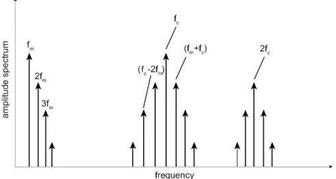
Fig. 1. Example of a sPWM spectrum
are very different, there are properties that they all have in common:
Modulation frequency:fm
Carrier frequency:fc
Harmonics:mfc±nfm
Afm ∝
M
2
AH ∝ C mJn(X)
where:
Af m= Amplitude of the modulation frequency; AH = Amplitude of the harmonics;
C = Amplitude factor;
M = Modulation index;
Jn(X)= The Bessel function of the first order for positive or integer values ofn;
X = The argument of the Bessel function;
m =1,2, . . . ,+∞;
[image:2.612.324.542.59.194.2]n =0,±1, . . . ,±∞;
Fig. 1 shows an example of such a power spectrum. From all these components, fm is the wanted output signal, whereas the rest of the signals are related to the used pulse train for generating the output. These high frequency components need to be considered carefully, as they are the main source of EMI for these kind of systems. The goal of the model is to approximate the location and strength of all the side harmonics. This is done by estimating the amplitude and bandwidth of each band of side harmonics.
A. Amplitude
As indicated in the previous section,
AH∝ C
mJn(X) (1)
Fig. 2. envelope of the asymptote of the Bessel function
where C is an amplitude factor and Jn(X) is the Bessel function of the first order for positive or integer values of
n. For leading- or trailing-edge modulation
C=Vp−p
π (2)
X =mπM (3)
and for double-edge modulation
C=2Vp−p
π (4)
X=mπM
2 (5)
where:
Vp−p = peak to peak, DC , supply voltage;
Since both descriptions of X increase linearly with m and
m → ∞, it can be concluded that X → ∞. Therefore it is assumed thatJn(X)can be approximated by the envelope of the asymptote of the Bessel function which is
Jn(X)≈ r
2
πX (6)
when n is fixed and |X| → ∞ [13]. Bessel functions with
n = 1, . . . ,4 and the proposed asymptote are shown in Fig. 2. This figure shows that the envelope follows the Bessel functions nicely after the first local maximum. Combining the approximations for C and Jn(X) this results in (7) for the estimation of the amplitude of the side harmonics.
AH≈ kVp−p
mπ r
2k
mπ2M (7)
Where k = 1 for leading- or trailing-edge modulation and
k= 2 for double-edge modulation.
B. Bandwidth
The bandwidth of a band of side harmonics is equal to the area in which most of the power is concentrated. The amount of power within a certain bandwidth is proportional to the amount of side harmonics that are taken into account, where the amplitude of the side harmonics is proportional to
band of side harmonics will be compared to the spectrum of a frequency modulated (FM) wave. Equation (8) shows the discrete spectrum for FM. The spectrum consists of a number of peaks spaced at fc±nfm wheren = 0,1, . . . ,∞ whose amplitude is proportional to Ac
2 Jn(β).
SF M = Ac
2
∞ X
−∞
Jn(β) [δ(f−fc−nfm) +δ(f +fc+nfm)]
(8) From FM theory we know that Carson’s rule gives the band-width over which98%of the power from the carrier is spread [14] shown in (9).
BF M ≈2 (fmβ+fm) (9)
Since FM and sPWM both have their energy spread propor-tional to harmonics weighed by Bessel functions, it is assumed that Carson’s rule is also applicable here for estimating the bandwidth of one band of side harmonics. Changing the argument from β to X and evaluating the result gives the bandwidth estimation shown in (10).
Bsh≈
2
kfmmπM+ 2fm (10)
Where again k = 1for leading- or trailing-edge modulation andk= 2for double-edge modulation.
C. Model
Now that the amplitude and the bandwidth of the bands of side harmonics can be estimated, they only have to be shifted to the right location in the frequency spectrum. The sPWM spectrum has the bands of side harmonics located around the carrier harmonics at mfc where m = 1,2, . . . ,∞. Each band will therefore be plotted using a rectangular function centered at the corresponding carrier harmonic. The width and the height of a rectangular function is equal to the predicted bandwidth and amplitude of that band. This results in m
rectangular functions, one for each side band. Combining these three properties results in the final model shown in (11).
SsP W M ≈
∞ X
m=1 AHrect
f−mfc Bsh
(11)
This results in two models for the sPWM spectrum, (12) for leading- or trailing-edge modulation and (13) for double-edge modulation.
Sl−tem≈
∞ X
m=1 Vp−p
mπ r
2
mπ2Mrect
f −mf
c
2fmmπM+ 2fm
(12)
Sdem≈
∞ X
m=1
2Vp−p mπ
r
4
mπ2Mrect
f −mf
c fmmπM+ 2fm
(13)
III. MEASUREMENTMETHOD
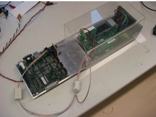
The validity of the model is experimentally verified by measuring sPWM signals and comparing those to the predicted spectra of the model. To see if the model is usable for analysis of real systems using sPWM modulation, a small test device is built. The device under test (DUT) consists of a FPGA based sPWM generator controlling a GaN half bridge to drive a load. This makes it possible to measure the sPWM control signal, the output signal and the radiated emission. Fig. 3 shows a picture of the DUT. One of the advantages in using a FPGA based sPWM generator is the flexibility it offers. The design specifications can be altered by changing the design parameters and reprogramming the FPGA. The sPWM generator discussed in [11] will be used during these measurements. With this sPWM generator it is possible to freely adjust the following parameters: carrier frequency (fc), modulation frequency (fm), modulation index (M). For this measurement, fc is varied between 24.4 kHzand1 MHz,fm is varied between 1 kHz and 100 kHz while not exceeding
fm < f10c, M is varied from 1
4 to 1, D is set to 0.5 and τ
is set to50 ns. Only bipolar double-edge modulated sPWM is generated. The half bridge module is a commercially available evaluation kit made by GaN systems. The half bridge module consists of the GS665MB-EVB evaluation platform accommo-dating the GS66508B-EVBDB daughter board, which features a rise and fall time off ≈10 ns. The half bridge is loaded by one of two different loads, where Z1= 27.2 Ω + 7.1µH and
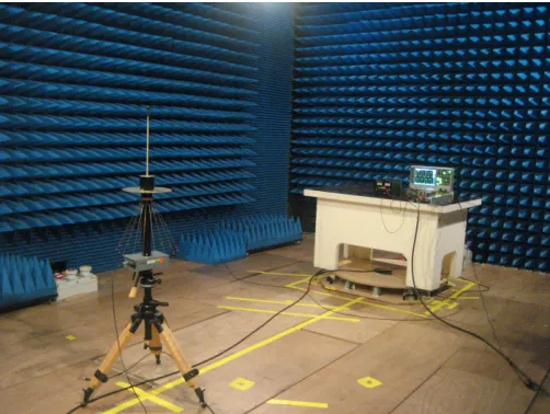
[image:3.612.312.563.410.599.2]Z2 = 10.2 Ω + 26µH. The measurements were performed at Thales Hengelo using anechoic chamber SEC II.
Fig. 3. The DUT, consisting of a sPWM generator and half bridge. The load can be connected to the panel
A. Radiated emission
The radiated signals were measured in time domain using a Pico Technology PicoScope 2208B computer oscilloscope using a measurement time of 100ms. The time domain signals are converted to the corresponding frequency spectrum using FFT conversion. The measurement bandwidth spans from 1 kHz, due to limitations on the measurement antenna, to 100 MHz, due to the measurement bandwidth of the Pico Scope. The results of these measurements are presented in the following section.
Fig. 4. Schematic representation of the used measurement setup for the radiated emission test
Where
A1 = A.R.A SAS-2/B measurement antenna; DUT = The test system;
V1 = Profilter SP430 power supply;
V2 = V3 = Delta SM 7020-D power supplies set at 35V DC;
Load = One of the two tested loads;
Fig. 5. Measurement setup inside the anechoic chamber, the oscilloscope is for monitoring outside the anechoic chamber
B. Conducted emission
[image:4.612.52.298.169.290.2]The output of the of sPWM generator and half bridge module were measured using the schematic representation of the measurement setup shown in Fig. 6. The same conditions as with the radiated emission measurement also apply here.
Fig. 6. Schematic representation of the used measurement setup for the sPWM and half bridge outputs
Where
DUT = The test system;
V1 = Profilter SP430 power supply;
V2 = V3 = Delta SM 7020-D power supplies set at 35V DC;
Load = One of the two tested loads;
IV. RESULTS
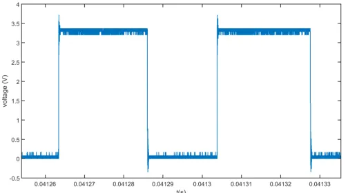
First, the results from the sPWM generator output will be presented. Fig. 7 and Fig. 8 show the spectra from the output of the sPWM generator withfc= 24.4 kHzandfm= 1 kHzbut different modulation index. The spectra are calculated by using FFT with a Hann window to increase the resolution. A section of the time domain signal used for calculating Fig. 7 is shown in Fig. 9. The time domain signal shows a nice ’square’ wave with∼10%overshoot and some noise. The overshoot usually introduces peaks at higher frequencies, but this is not seen in the spectrum of Fig. 7. Looking at the spectra around the bands of side harmonics in Fig 7 and Fig. 8, it appears that the even harmonics are suppressed, this is one of the characteristics of double-edge modulation. Due to the symmetry in the carrier wave, harmonics cancel each other whenm+n=even. This is also visible in all other spectra. Comparing the amplitude of the harmonics from Fig. 7 and Fig. 8 with each other, one sees that the slope of the decay of harmonics is the same for both modulation indices, only the amplitude is6 dBhigher for
M = 0.25compared to M = 1. While the model does scale the amplitude properly for the different modulation indices, the slope is a little bit too steep. Where the model shows a slope of −30 dB/decade the actual slope looks more like
[image:4.612.49.300.423.612.2]Fig. 7. sPWM spectrum withM= 0.25,fm= 1 kHz,fc= 24.4 kHz
Fig. 8. sPWM spectrum withM= 1,fm= 1 kHz,fc= 24.4 kHz
a band of side harmonics at high harmonics is required, the slope should be modified. This is done by using
Ah≈ kVp−p
mπ
3
r k
mπ2M (14)
when m >10. This approximates the slope better but results in an underestimated amplitude at low harmonics.
Fig. 10, 11 and Fig. 12 show the output of the sPWM generator wth fc = 24.4 kHz and M = 1 but different fm.
Fig. 9. Section of the time signal from the sPWM generator withM= 0.25,
fm= 1 kHz,fc= 24.4 kHz
Fig. 10. sPWM spectrum withM= 1,fm= 1 kHz,fc= 1 MHz
Fig. 11. sPWM spectrum withM= 1,fm= 10.6 kHz,fc= 1 MHz
[image:5.612.50.565.230.378.2]A section of the time domain signal of Fig. 10 is shown in Fig. 13. Although there is no ringing, some ’bounce’ is observed, this was determined to be coupling from the output to the input. This is probably the cause for the increased harmonics between30 MHzand100 MHzin Fig. 10. All three measurements show this in the spectrum. Fig. 10 shows a spectrum of very small peaks at mfc due to the high ratio of fc/fm = 1000. Since B ∝ fm, the bandwidth is very small. Fig. 11 shows wider peaks due to the higher modulation frequency since the ratio of fc/fm ≈ 100. As with Fig. 7 and Fig. 8, the amplitude from bands of harmonics below the tenth harmonic are overestimated whereas higher harmonics are underestimated. Fig. 12 shows almost all overlapping bands due to the small ratio of fc/fm = 10. Comparing the bandwidth of bands between Fig. 10, Fig. 11 and Fig. 8 confirms that the bandwidth increases with fm. It seems that the bands contain most of the energy, thus the bandwidth is modelled correctly in all three figures. Comparing the amplitude of the bands of side harmonics between Fig. 8 and Fig. 10 shows that the amplitude of the m-th band is the same for both as expected. It also shows that an increased
[image:5.612.49.301.547.687.2]Fig. 12. sPWM spectrum withM= 1,fm= 100 kHz,fc= 1 MHz
Fig. 13. Section of the time signal from the sPWM generator withM= 1,
fm= 1 kHz,fc= 1 MHz
different loads. Fig. 16 shows a section of the time signal of Fig. 14 with highlighted regions A and B. The time signal shows a lot of distortion on the output wave resulting in a envelope of frequency fm. Overshoot is observed in region A, indicating possible peaks at higher frequencies. Slewing is observed in region B, the output voltage does not reach the power supply rail due to the finite rise time of the output. This indicates reduced harmonics at higher frequencies. These two phenomena are a probable cause for the peaks and dips above 20 MHz shown in Fig.14 and Fig. 15. For frequencies below 20 MHz, the estimated amplitude and bandwidth of the bands coincide with the amplitude and bandwidth of the measured bands. Above 20 MHz, it is obvious that the model does not incorporate the previous stated parasitics.
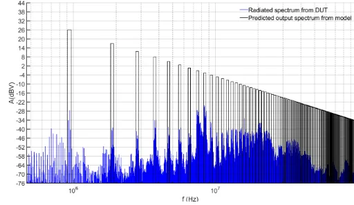
Finally, the radiated spectrum is compared to the predicted output. Fig. 17 and Fig. 18 show these spectra for M = 1,
fm= 10.6 kHz,fc = 1 MHzand different loads. Comparing the received spectrum from Fig. 17 to Fig. 18 shows that the radiation efficiency is influenced by the load and causes differences of up to 12 dB at 2, 3 and 8 MHz. Assuming that the modelled spectrum approximates the output spectrum accurately, the radiation efficiency of the device can be ap-proximated by comparing the output with the received field strength. Doing this for Fig. 17 to Fig. 18 would approximate the radiation efficiency within 6 dB up to 20 MHz. Above
Fig. 14. Output spectrum with M = 1,fm = 10.6 kHz,fc = 1 MHz, load=27.2 Ω
Fig. 15. Output spectrum with M = 1,fm = 10.6 kHz,fc = 1 MHz, load=10 Ω
[image:6.612.51.299.230.371.2] [image:6.612.314.564.296.448.2] [image:6.612.314.563.521.667.2]Fig. 17. Radiated spectrum with M = 1,fm= 10.6 kHz,fc= 1 MHz, load=27.2 Ω
Fig. 18. Radiated spectrum with M = 1,fm= 10.6 kHz,fc= 1 MHz, load=10 Ω
20 MHz errors of up to20 dB would occur due to the peaks and dips shown in Fig. 14 and Fig. 15. The radiated spectrum from Fig. 18 shows a radiation peak at 8 MHz. Shifting the carrier frequency down with62 kHzresults in the spectrum of Fig. 19. By shifting carrier frequency, the maximum amplitude of the received signal around 8 MHz is lowered by at least 6 dB. This is a good example of minimizing EMI by parameter variation. The bandwidth and location of the bands of side harmonics are correctly modelled again.
V. CONCLUSION
[image:7.612.307.563.51.199.2]The amplitude of a band of side harmonics, estimated by the model, shows a trade-off between the accuracy at low and higher harmonics of the carrier wave. The amplitude is overestimated at lower harmonics whereas the amplitude is underestimated at higher harmonics. This can be compensated at higher frequencies by using the modified slope. Since the model is based on ideal 2-level sPWM signals, parasitics are not taken into account, making the model less useful for situations where a lot of distortion is present in the sPWM waveform. But, as shown in Fig. 7 and Fig. 8, the model predicts the spectrum of a well behaved sPWM wave accurately. Given the above stated limitations, the model is use-able for rough estimation of the spectrum from a sPWM
Fig. 19. Radiated spectrum withM= 1,fm= 10.6 kHz,fc= 938 kHz, load=10 Ω
wave. In devices consisting of several submodules, the model can be used for placing bands of side harmonics at points in the frequency spectrum that are not used by other subsystems. This can minimize the interference between subsystems. A final use may be for the derivation of optimal parameters of a sPWM generator for reducing EMI. When a model or measurement of the radiation pattern of the device is known one can calculate the radiated emission. By shifting the harmonics regions where the radiation efficiency is low, EMI radiation can be reduced as shown in Fig. 18 and Fig. 19.
ACKNOWLEDGEMENT
The authors like to thank the Dutch research organization for scientific research (NWO) for funding the joint research project Smart Grid.
REFERENCES
[1] J. A. Ferreira, “The multilevel modular dc converter,”IEEE Transactions on Power Electronics, vol. 28, no. 10, pp. 4460–4465, Oct 2013. [2] ——, “Nestled secondary power loops in multilevel modular converters,”
in 2014 IEEE 15th Workshop on Control and Modeling for Power Electronics (COMPEL), June 2014, pp. 1–9.
[3] M. Lakka, E. Koutroulis, and A. Dollas, “Development of an fpga-based spwm generator for high switching frequency dc/ac inverters,” IEEE Transactions on Power Electronics, vol. 29, no. 1, pp. 356–365, Jan 2014.
[4] L. T. Duc and K. Wada, “Experimental verification of 1 mhz pwm inverter for generating high frequency sinusoidal current,” in2016 IEEE 8th International Power Electronics and Motion Control Conference (IPEMC-ECCE Asia), May 2016, pp. 8–12.
[5] J. Liu, W. Yao, Z. Lu, and X. Xu, “Design and implementation of dsp based high-frequency spwm generator,” in2016 IEEE 8th International Power Electronics and Motion Control Conference (IPEMC-ECCE Asia), May 2016, pp. 597–602.
[6] D. Navarro, . Luca, L. A. Barragn, J. I. Artigas, I. Urriza, and . Jimnez, “Synchronous fpga-based high-resolution implementations of digital pulse-width modulators,” IEEE Transactions on Power Electronics, vol. 27, no. 5, pp. 2515–2525, May 2012.
[7] J. Biela, M. Schweizer, S. Waffler, and J. W. Kolar, “Sic versus si-evaluation of potentials for performance improvement of inverter and dc-dc converter systems by sic power semiconductors,”IEEE Transactions on Industrial Electronics, vol. 58, no. 7, pp. 2872–2882, July 2011. [8] T. Nomura, M. Masuda, N. Ikeda, and S. Yoshida, “Switching
[image:7.612.51.300.237.386.2][9] J. i. Itoh, T. Araki, and K. Orikawa, “Experimental verification of an emc filter used for pwm inverter with wide band-gap devices,” in2014 International Power Electronics Conference (IPECHiroshima 2014 -ECCE ASIA), May 2014, pp. 1925–1932.
[10] F. Zare, “Emi issues in modern power electronic systems,” The IEEE EMC Society Newsletters, no. 221, pp. 53–58, 2009. [Online]. Available: https://eprints.qut.edu.au/31175/
[11] N. Moonen, F. Buesink, and F. Leferink, “Emi reduction in spwm driven sic converter based on carrier frequency selection,” in2017 International Symposium on Electromagnetic Compatibility - EMC EUROPE, Sept 2017, pp. 1–5.
[12] F. Vasca and L. Iannelli,Dynamics and control of switched electronic systems: advanced perspectives for modeling, simulation and control of power converters. Springer, 2012.
[13] M. Abramowitz and I. A. Stegun,Handbook of mathematical functions: with formulas, graphs, and mathematical tables. Courier Corporation, 1964, vol. 55.