DOI: 10.4236/jamp.2019.711192 Nov. 13, 2019 2796 Journal of Applied Mathematics and Physics
The Mapping and Optimization Method of
Quantum Circuits for Clifford + T Gate
Xianya He
1, Zhijin Guan
1,2*, Fei Ding
11School of Information Science and Technology, Nantong University, Nantong, China 2Jiangsu Key Laboratory of Asic Design, Nantong University, Nantong, China
Abstract
In order to solve the fault tolerance and reliability problems of quantum cir-cuit, a series of structural equivalence rules and optimization operation strat-egies of quantum circuit are proposed to minimize the number of T gates, in-crease T gate depth, minimize circuit level, reduce fault tolerance implemen-tation costs and increase circuit reliability. In order to satisfy the nearest neighbor constraints of some quantum systems, a LNN (linear nearest neighbor) arrangement algorithm based on Clifford + T gate quantum circuit is presented. Experiments are done on some benchmarks of RevLib, the re-sults show that the optimization rate of most functions and the running time of the algorithm are better than those of the existing literature.
Keywords
Quantum Circuit, Clifford + T Circuit, Quantum Cost
1. Introduction
Quantum circuits are an important model of quantum computing. The integra-tion and optimizaintegra-tion of quantum circuits is of great significance [1] [2] [3]. In recent years, the Clifford + T gates [4] [5] [6] have been used in some typical quantum circuits. Due to the importance of fault tolerance in quantum compu-ting [7] [8], and the fault-tolerant implementation cost of T gates may exceed the implementation cost of Clifford Gate by 100 times or more [4]. Therefore, minimizing the number of T gates is critical to optimizing the T depth of a quantum circuit.
Due to the limitation of quantum techniques, it is required that the control bit and target bit of the 2-qubit gates are physically adjacent, that is the Linear Nearest Neighbor (LNN) constraint required to be considered [9] [10] [11]. This How to cite this paper: He, X.Y., Guan,
Z.J. and Ding, F. (2019) The Mapping and Optimization Method of Quantum Circuits for Clifford + T Gate. Journal of Applied Mathematics and Physics, 7, 2796-2810.
https://doi.org/10.4236/jamp.2019.711192
DOI: 10.4236/jamp.2019.711192 2797 Journal of Applied Mathematics and Physics paper considers the mapping of NCV circuits to equivalent circuits composed of Clifford + T gates, especially optimizing T-count and T-depth, reducing circuit depth, satisfying the constraints of certain quantum architecture, reducing the cost of fault tolerance quantum circuit, and increasing circuit reliability.
2. Background
2.1. Quantum Gate and Quantum Circuit
The basic unit of operation in a quantum system is a qubit, which is similar to a bit in classical computer system. Qubits can represent states 0 and 1, represented by the symbols |0> and |1> respectively. Qubits can also represent an infinite number of state vectors |φ> (called quantum superposition states) between 0 and 1, expressed as:
0 1
ϕ =α +β (1)
where α and
β
are complex numbers and satisfy the condition2 2
1
α
+
β
=
.The operation of the qubit is equivalent to superimposing a unitary matrix U on the state vector of the qubit. The logic gates that operate on qubits in quan-tum circuits are called quanquan-tum gates [12], and each quanquan-tum gate can be represented by a 2n-order unitary matrix, where n represents the number of qu-bits.
A quantum circuit cascaded by quantum gates is called a quantum circuit. Some specific quantum gates that make up a quantum circuit are called quantum gate libraries [13]. The NCV gate library contains quantum gates such as NOT, CNOT, V, and V+ [9]. The Clifford + T gate library includes quantum gates such as NOT, CNOT, H, S, S+, T, and T+ which is shown in Table 1. The circuit cas-caded only by Clifford + T quantum gates is called Clifford + T circuit. The Clif-ford + T gate libraries are adopted by many quantum physics architectures [14].
The one-dimensional n-qubit circuit has n horizontal lines, respectively representing n quantum bit lines, which are sequentially recorded as
1 2
{ , , , }n
l= l l … l from top to bottom. The position of the left to right quantum
gate in the line (can be regarded as a vertical line from left to right) indicates the time sequence of the line execution, which is recorded as h={ , , , }h h1 2 …hm . Figure 1 is an example of representation of quantum circuit. There l={1,2,3,4}
and h={1,2,3, ,21}… .
2.2. Quantum Gate Decomposition
DOI: 10.4236/jamp.2019.711192 2798 Journal of Applied Mathematics and Physics Figure 1. A example of representation of quantum circuit.
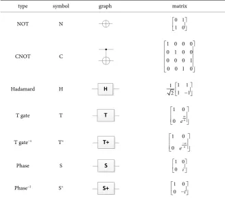
Table 1. Clifford + T gate library.
type symbol graph matrix
NOT N 1 00 1
CNOT C
1 0 0 0 0 1 0 0 0 0 0 1 0 0 1 0
Hadamard H 121 11 −1
T gate T
4 1 0 0 eiπ
T gate−1 T+
4 1 0 0 e−iπ
Phase S 1 00 i
Phase−1 S+ 1 0
0 i
−
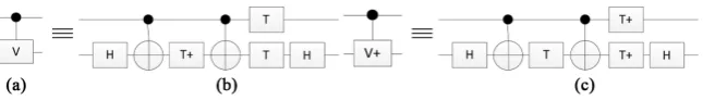
Figure 3(a). A V+ gate can be decomposed into seven gates as shown in Figure 3(b), and the equivalent circuit can be obtained by further simplification as shown in Figure 3(c).
2.3. Clifford + T Circuit Structure
Definition 1: In a one-dimensional quantum circuit, a sequence of quantum gates that can be operated in parallel is called a circuit level. If two or more quantum gates can be combined together in a circuit, their qubits can operate in parallel without disjoint, and these quantum gates are said to form a grouped.
Definition 2: In a one-dimensional circuit, the circuit depth is the number of levels in the circuit.
Definition 3: The T-depth of the Clifford + T circuit is the number of T or T+ gates contained on different qubit lines in one level of the circuit.
DOI: 10.4236/jamp.2019.711192 2799 Journal of Applied Mathematics and Physics Figure 2. Decomposition of Toffoli gate.
Figure 3. Decomposition of V gate and V+ gate. (a) Decomposition of V gate; (b) De-composition of V+ gate; (c) Equivalent circuit for the (b) reduction.
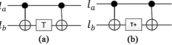
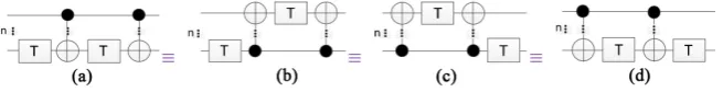
The two control bits and the two target bits of the two CNOT gates are on the same qubit line, and the T (or T+) gate is between the two target bits.
Figure 4(a) and Figure 4(b) are represented as CTC (T) and CTC (T+) re-spectively for ease of use. Where line la is called the control bit line of the CTC-structure, and line lb is called the target bit line of CTC-structure. If the control bit line of the CTC-structure is line i, the target bit line is line j, and the two CNOT gates are located on h1 and h2 respectively (h h1= 2−2), then the CTC-structure can be expressed as CTCh h1 2, ( , )i j .
Definition 5: The depth of the CTC-structure refers to the number of T (or
T+) gates that can be operated in parallel in the CTC-structure.
Definition 6: If the depth of the CTC-structure is equal to the number of the circuit input/output qubits, then this CTC-structure is said to be full.
3. Decomposition and Optimization of the Quantum Circuits
In order to optimize quantum circuits, the quantum gates and related sub-line structures in the Clifford + T circuit are analyzed and discussed in this section.3.1. Relevant Properties
The following properties 1 - 3 [5] can be verified by the matrix representation of the quantum gates, which are multiplied by matrices to obtain the results of their interactions.
Property 1: (a) Two adjacent T-gates are equivalent to a S-gate. Two adjacent
T+-gates are equivalent to a S+-gate.
Property 2: A CNOT gate is equivalent to two consecutive V-gates which have same control bit line and target bit line. A CNOT gate is also equivalent to two consecutive V+-gates which have same control bit line and target bit line.
[image:4.595.215.538.139.185.2]DOI: 10.4236/jamp.2019.711192 2800 Journal of Applied Mathematics and Physics Figure 4. Two forms of CTC-structure. (a) CTC(T) structure; (b) CTC (T+) structure.
if the target bits are on the same qubit line, and their combinations are switched. Property 5: If the T-gate (or T+-gate) and the 2-qubit gate control bit are on the same qubit line and adjacent to each other, then the combination of the
T-gate (or T+-gate) and the 2-qubit gate on the left and right sides of the control bit of the 2-qubit gate are equivalent [5].
Property 6 [5]: For two CTC(T) structures, if the control line of a CTC(T) structure is the target line of the other CTC(T) structure, then the two CTC(T) structures are equivalent. Analogously, For two CTC(T+) structures, if the con-trol line of a CTC(T+) structure is the target line of the other CTC(T+) structure, then the two CTC(T+) structures are equivalent.
Property 7 [5]: The combination of the 2-qubit gate and the CTC(T) struc-ture are equivalent for the right and the left of CTC(T) structure, if the control bit of the 2-qubit gate is on the target bit line of the CTC(T) structure and the target bit of the 2-qubit gate is not on the line crossed by CTC(T). The combina-tion of the 2-qubit gate and the CTC(T+) structure are equivalent for the right and the left of CTC(T+) structure, if the control bit of the 2-qubit gate is on the target bit line of the CTC(T+) structure and the target bit of the 2-qubit gate are not on the line crossed by CTC(T+).
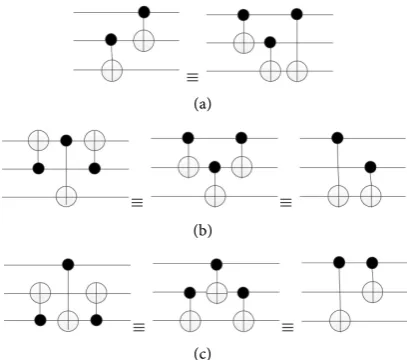
Property 8: The subcircuit of the CNOT gate combination is equivalent as shown in Figures 5(a)-(c).
The equivalence of the above subcircuits can be easily verified by the truth ta-ble.
Conclusion 1: The combination of two adjacent T-gates and 2-qubit gate are equivalent on the right and the left of control bit of this 2-qubit gate.
The combination of two adjacent T+-gates and 2-qubit gate are equivalent on the right and the left of control bit of 2-qubit gate.
The above inferences are readily available based on property 5.
Generally, the arbitrary combination of m (m ≥ 1) 2-qubit gates and n (n ≥ 1)
T-gates (or T+-gates) are equivalent, if the control bits of m (m ≥ 1) 2-qubit gates and n (n ≥ 1) T-gates (or T+-gates) are on the same qubit line.
Conclusion 2: According to property 1, the S-gate (or S+-gate) distributed on the left and right sides of the control bit is equivalent for a combination of an S-gate (or S+-gate) on the control bit line of a two-qubit gate and the two-qubit gate. It can be seen from the conclusion 1.
Conclusion 3: The combination of single quantum gate (T, T+, S, S+) located on the left and right side of CTC structure is equivalent if the single quantum gate is on the same quantum bit line of CTC-structure.
DOI: 10.4236/jamp.2019.711192 2801 Journal of Applied Mathematics and Physics (a)
(b)
[image:6.595.271.475.70.250.2](c)
Figure 5. Equivalent variations of CNOT gate sequence. (a) The first equivalent case; (b) The second equivalent case; (c) The third equivalent case.
its control bit line and target bit line are equivalent. 2) Any combinations of the CTC-structure with the T+-gates on its control bit line and target bit line are equivalent.
Proof: As long as proof 1), then 2) is available as the same.
1) According to the Property 6, the CTC-structure interchange control bit line with target bit line is equivalent, so the combination of a T gate and a CTC-structure on the same qubit line is also equivalent. As show in Figure 6 that Figure 6(a) is equivalent to Figure 6(b);
2) According to the Property 5, the T gate of Figure 6(b) can be moved to the right side of the first CNOT gate. Similarly, it can be moved to the right side of the second CNOT gate to get Figure 6(c). As show in Figure 6 that Figure 6(b) is equivalent to Figure 6(c);
3) According to the Property 6, the CTC-structure interchange control bit line with target bit line is equivalent, therefore, the combination of the CTC-structure and the T gate on the same bit line is also equivalent. As show in Figure 6 that Figure 6(c) and Figure 6(d) are equivalent.
QED ■ Corollary 1: The combination of S-gate (or S+-gate) and CTC-structure is equivalent when S-gate (or S+-gate) is on the left or right sides of the target posi-tion of the CTC-structure according to property 1 and theorem 1.
Theorem 2: In an 1-dimensional quantum circuit, let V′ ={ , }V V+ , if there are consecutive mV-gates and nV+-gates, the control bit line of V' and the target bit line of V' are same respectively, then the target bit line of the m + nV'-gates can decompose into sub-circuit structure and the number of quantum gates are:
, ,
H H m n is even
H T H m n is odd
+ Σ + −
+ Σ + +′ −
(2)
DOI: 10.4236/jamp.2019.711192 2802 Journal of Applied Mathematics and Physics Figure 6. Equivalent exchange of T and CTC-structures. (a) Original circuit; (b) Circuit after CTC-structure flip; (c) Circuit after T gate movement; (d) Final circuit.
, ,
m n is even T m n is odd
Σ −
′
Σ + −
(3)
where T′ ={ , }T T+ , S′ ={ , }S S+ ,
( )
( )
CTC CTC
2
m T+ n T m n S′
Σ = − ∗
∗ + ∗ + .
Proof: In an 1-dimensional quantum circuit, it is assumed that there are k
quantum bit lines l (i.e. the input/output of the quantum line is k), that is,
1 { , , , }1 2 k
L = l l … l . If there are consecutive m target bits of V-gates and n target
bits of 𝑉𝑉+-gates on the i-th quantum bit line, i∈{1,2, , }… k . Let
1, ,2 1
{ , } , m, m , , m n
V′= V V+ =<V V′ ′…V V′ ′+ …V′+ >, then:
The target bit line of V-gate in V′ can be decomposed into:
( )
CTC
H
+
T
++ +
T H
(4)The target bit line of V+-gate in V′ can be decomposed into:
( )
CTC
H+ T +T++H (5)
It can be seen that when m, n ≥ 1, continuous m + nV'-gates are decomposed, and m + n − 1 pair of H-gates are adjacent on the target bit line of CTC-structure. In (1) and (2), the first H-gate and the last H-gate are the re-maining, and there are m + n CTC-structures and mT-gates and nT+-gates be-tween this two H-gates. By the theorem 1, these mT-gates and nT+-gates can be moved so that they are adjacent. So there have:
1) When m>n, there are n T-gates and nT+-gates are eliminated and ⌊(m −
n)/2⌋ pairs of T-gates are replaced by ⌊(m − n)/2⌋ S-gates. If m-n is an even number, all T gates are replaced; if m-n is an odd number, then remain a T-gate. The target bit line of V′-gate can eventually be decomposed into:
( )
( )
( )
( )
CTC CTC ,
2
CTC CTC ,
2
H m T n T S H m n is even
H
m n
m n
m T n T S T H m n is odd
+ + + ∗ + ∗ + ∗ + − − − + ∗ + ∗ + ∗ + + − (6)
2) When m = n, all T-gates and T+-gates are eliminated. The target bit line of
V′-gate can eventually be decomposed into:
( )
( )
CTC
CTC
H m
+ ∗
T
++ ∗
n
T
+
H
(7) 3) When m < n, there are m T-gates and m T+-gates are eliminated, and
) / 2
(n m−
pairs of T+-gates are replaced by (n m− ) / 2 S+-gates. If n-m is
re-DOI: 10.4236/jamp.2019.711192 2803 Journal of Applied Mathematics and Physics maining a T+-gate. The target bit line of the V′-gate can be eventually decom-posed into:
( )
( )
( )
( )
CTC CTC ,
2
CTC CTC ,
2
n m
H m T n T S H n m is even
n m
H m T n T S T H n m is odd
+ + + + + + ∗ + ∗ + − ∗ + − − + ∗ + ∗ + ∗ + − + (8)
The control bit of V-gate and V+-gate in V′ can be decomposed into the form of
CTC
( )
T
++
T
and( )
CTC T +T+ respectively at the control bit line.
The control bit of mV-gates and nV+-gates in V′ may be distributed on the
{
}
2 1, , , , ,i 1 i 1 k
L = l … l l− + …l . When m, n ≥ 1, after successive m + nV' gates are
de-composed, there are a total of m + n CTC-structures, mT-gates and nT+-gates on all control bit lines. Among them, the l lj( j∈L2) qubit line has m Tj -gates,
j
n T+-gates and
j j
m +n CTC-structures, where k 1 j j
m=
∑
=m , k 1 j jn=
∑
= n , j i≠ .By theorem 1, these m Tj -gates and n Tj +-gates can be moved to be adjacent, so:
1) When mj>nj, there are n Tj -gates and n Tj +-gates are eliminated;
) /
(
m n
j−
j2
pairs of T-gates are replaced by
(
m n
j−
j) /
2
S-gates. If j jm −n is an even number, all T-gates are replaced, and if mj−nj is an odd number, then remain a T-gate. The control bit line of the V′-gate can be finally
decomposed into:
( )
( )
( )
( )
CTC CTC ,
2
CTC CTC ,
2
j j
j j j j
j j
j j j j
m n
m T n T S m n is even
m n
m T n T S T m n is odd
+ + − + + − − + + + − ∗ ∗ ∗ ∗ ∗ ∗ (9)
2) When mj =nj, all m Tj -gates and m Tj +-gates are eliminated. The con-trol bit line of V′-gate can be finally decomposed into:
( )
( )
CTC
CTC
j j
m
∗
T
++ ∗
n
T
(10)3) When mj<nj , m Tj gates and m Tj + -gates are eliminated, and
) /
(
n m
j−
j2
pairs of T+-gates are replaced by
(
n m
j−
j) /
2
S+-gates. If j jn −m is an even number, all T+-gates are replaced and if j j
n −m is an odd number, then remain a T+-gate. The control bit line of the V′-gate can be final-ly decomposed into:
( )
( )
( )
( )
CTC CTC 2 CTC CTC 2 , , j j j j j j j j n mm T n T S n m is even
n m
m T n T S T n m is odd
DOI: 10.4236/jamp.2019.711192 2804 Journal of Applied Mathematics and Physics (a)
[image:9.595.215.534.73.213.2](b)
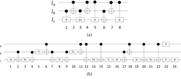
Figure 7. Quantum circuit Clifford + T gate decomposition example. (a) Original NCV circuit; (b) Decomposed Clifford + T circuit.
on the same qubit line lc. The circuit after decomposition is shown in Figure 7(b) where the second H gate and Tc gate generated by G1 are eliminated re-spectively with the first H gate and Tc+ gate generated by G3, the second H gate and Tc+ gate generated by G3 are eliminated respectively with the first H gate and Tc gate generated by G5, while the H gate generated by G8 cannot cancel out with the H gate generated by G5 because of the blocking of the G6 target bit. The Ta generated by G5 and G8 respectively can be merged into Sa.
3.2. Algorithm for Decomposition of NCV Circuit
In order to obtain the quantum circuit composed of Clifford + T gate, using the equivalent circuit given in Figure 3 and the related theory of theorem 2 to de-compose NCV circuit.
The circuit is initially optimized with the relevant properties in the decompo-sition process. The decompodecompo-sition algorithm is shown in Algorithm 1.
3.3. Depth Maximization of the CTC-Structure
In order to deepen the depth of the CTC-structure, reduce the depth of the cir-cuit, improve the parallelism of the circir-cuit, the decomposed Clifford + T circuit need to be structured and the main goal is to make the depth of each CTC-structure equal to the number of qubits (That is to say, make the CTC-structure to be fully occupied). The CTC-structure depth deepening algo-rithm is shown in Algoalgo-rithm 2.
3.4. Depth Optimization of Circuit
After deepening the depth of the CTC-structure of the circuit, there will be many adjacent CNOT gates. The optimization of continuous CNOT gates can reduce the number of gates. Algorithm 3 is CNOT optimization algorithm.
4. Quantum Circuit Synthesis Satisfying Constraints
4.1. Some Constraints on Quantum Circuits
DOI: 10.4236/jamp.2019.711192 2805 Journal of Applied Mathematics and Physics Algorithm 1. NCV decomposition algorithm.
DOI: 10.4236/jamp.2019.711192 2806 Journal of Applied Mathematics and Physics Algorithm 3. CNOT optimization algorithm.
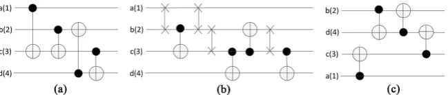
gates are required to satisfy linear nearest neighbor constraints. In a quantum logic circuit, to exchange the logic values of certain two circuits, it can generally be realized by inserting a SWAP-gate. The SWAP-gate also needs to satisfy the linear nearest neighbor in the nearest neighbor constrained quantum circuit, it is called the nearest neighbor SWAP gate (NNS gate) [7]. An NNS gate is equiva-lent to three cascades of CNOT gates that satisfy the linear nearest neighbor ar-chitecture, as shown in Figure 8(a). Some quantum circuit physical structures require even stronger constraints. For example, IBM QX [17] [18] requires that the CONT gates in different directions be flipped through the H gate to be in the same direction (control bits and target bits are on two qubits), as shown in Fig-ure 8(b). Converting a non-LNN Clifford + T circuit into an LNN Clifford + T circuit is usually done by inserting several NNS gates, as shown in Figure 9. Figure 9(a) is a non-LNN circuit, Figure 9(b) is equivalent LNN circuit by in-sert SWAP gates, Figure 9(c) is equivalent form of NNS gate.
4.2. Synthesis Algorithm
It can be seen from the literature [1] that the linear nearest neighbor cost of the 2-qubit gate G in a quantum circuit is:
1
nnc C T
G = l −l − (12)
DOI: 10.4236/jamp.2019.711192 2807 Journal of Applied Mathematics and Physics Figure 8. Equivalent form of NNS gate. (a) Equivalent form of a SWAP gate; (b) CNOT flips to the same direction.
Figure 9. (a) Non-LNN circuit; (b) Equivalent LNN circuit by inserting SWAP gates; (c) Equivalent LNN circuit by rearranging the quantum lines.
1
1,(1 )
K nnc i
N i
CC G K N
N
=
− +
′ =
∑
× < ≤ (13)where N is the number of quantum gates in the Clifford + T circuit and K is the linear nearest neighbor cost calculation coefficient of the circuit.
This paper presents an adaptive Clifford + T circuit neighborhood optimiza-tion algorithm, such as Algorithm 4. The optimized Clifford + T circuit is scanned from left to right, and all LNN schemes are listed for the first non-LNN 2-qubit gate is encountered. Calculate the CC′ of the remaining circuit after
each scheme is executed, select the scheme with the smallest CC′, insert the
NNS gates into the circuit one after the other, then continue to scan the remain-ing circuits, and iteratively execute the above steps until all the quantum gates reached LNN. The algorithm is executed for all coefficients K, and the scheme with the least number of inserted switching gates is recorded for output.
The time complexity of the algorithm is O L N K( × × ), where L is the
quan-tum number. For small-scale circuits, try all the coefficients K to find the optim-al solution. For large-scoptim-ale circuits, K can be reduced to a constant term in order to reduce algorithm runtime.
5. Experiment and Result Analysis
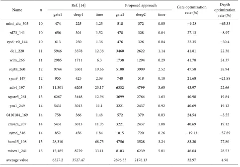
[image:12.595.212.537.167.236.2]DOI: 10.4236/jamp.2019.711192 2808 Journal of Applied Mathematics and Physics Name n Gate optimization rate (%) optimization
rate (%) gate1 deep1 time gate2 deep2 time
mini_alu_305 10 474 225 1.25 518 372 0.05 −9.28 −65.33 rd73_141 10 656 301 1.52 478 328 0.04 27.13 −8.97 sys6−v0_144 10 613 250 1.36 476 326 0.04 22.35 −30.4 dc1_220 11 5946 3378 12.38 3460 2622 1.14 41.81 22.38 wim_266 11 2985 1711 6.3 1738 1294 0.29 41.78 24.37 sqrt8_260 12 9744 5501 19.66 5108 3909 2.52 47.58 28.94 sym9_147 12 955 425 2.08 748 518 0.10 21.68 −21.88
adr4_197 13 11,301 6205 23.17 6332 4799 3.65 43.97 22.66 squar5_261 13 6267 3448 12.96 3699 2764 1.63 40.98 19.84 pm1_249 14 5431 3013 11.1 3221 2437 0.92 40.69 19.12 0410184_169 14 758 366 1.48 572 379 0.03 24.54 −3.55 cm42a_207 14 5431 3013 11.95 3221 2437 1.08 40.69 19.12 sym6_316 14 852 456 1.84 1015 720 0.26 −19.13 −57.89 ham15_108 15 28,310 68.75 4756 3528 3.24 83.20 77.80 misex1_241 15 15,185 8729 33.11 8103 6239 5.81 46.64 28.53 average value 6327.2 3527.47 2896.33 2178.13 32.97 4.98
Algorithm 4. LNN arrangement algorithm based on quantum weight.
[image:13.595.57.541.88.425.2]DOI: 10.4236/jamp.2019.711192 2809 Journal of Applied Mathematics and Physics
6. Conclusion
Due to the limitations of some quantum techniques, there are special require-ments for the use of quantum gates in quantum circuits, and the linear nearest neighbor constraints are required for the physical positions of the control bits and target bits of the 2-qubit gates. The main work of this paper is to map the NCV circuit to the equivalent circuit composed of Clifford + T gate, optimize the quantum gate number and T depth, reduce the circuit depth, propose a se-ries of circuit structure equivalence rules and optimization operation strategies. The CNOT gate neighbor algorithm of the Clifford + T gate quantum circuit sa-tisfies the CNOT constraint imposed by the architecture. In the related proper-ties and operation methods proposed in this paper, due to the limitation of H gate, the optimization of the circuit will have a great impact. How to lay out the position of the H gate is an important part of future work research.
Conflicts of Interest
The authors declare no conflicts of interest regarding the publication of this pa-per.
References
[1] Abdessaied, N. and Drechsler, R. (2018) Reversible and Quantum Circuits Optimi-zation and Complexity Analysis. Springer Nature.
[2] Wille, R., Keszocze, O., Walter, M., Rohrs, P., Chattopadhyay, A. and Drechsler, R. (2016) Look-Ahead Schemes for Nearest Neighbor Optimization of 1d and 2d Quantum Circuits. Asia and South Pacific Design Automation Conf., 292-297.
https://doi.org/10.1109/ASPDAC.2016.7428026
[3] http://www.jku.at/iic/eda/ibm_qx_mapping
[4] Biswal, L., Bandyopadhyay, C., Wille, R., et al. (2016) Improving the Realization of Multiple-Control Toffoli Gates Using the NCVW Quantum Gate Library. Interna-tional Conference on VLSI Design & InternaInterna-tional Conference on Embedded Sys-tems. https://doi.org/10.1109/VLSID.2016.23
[5] Miller, D.M., Soeken, M. and Drechsler, R. (2014) Mapping NCV Circuits to Opti-mized Clifford + T Circuits. Reversible Computation. Springer International Pub-lishing. https://doi.org/10.1007/978-3-319-08494-7_13
[6] Saeedi, M., Wille, R. and Drechsler, R. (2010) Synthesis of Quantum Circuits for Linear Nearest Neighbor Architectures. Quantum Information Processing.
https://doi.org/10.1007/s11128-010-0201-2
[7] Xueyun, C., Zhijin, G. and Weiping, D. (2018) Mapping from Multiple-Control Toffoli Circuits to Linear Nearest Neighbor Quantum Circuits. Quantum Informa-tion Processing, 17, 169. https://doi.org/10.1007/s11128-018-1908-8
[8] Abhari, A.J., Faruque, A., Dousti, M.J., Svec, L., Catu, O., Chakrabati, A., Chiang, C.-F., Vanderwilt, S., Black, J. and Chong, F. (2012) Scaffold: Quantum Program-ming Language. Technical Report, Princeton Univ Nj Dept of Computer Science. [9] Wille, R., Lye, A. and Drechsler, R. (2014) Exact Reordering of Circuit Lines for
DOI: 10.4236/jamp.2019.711192 2810 Journal of Applied Mathematics and Physics tion Conf., 41-46. https://doi.org/10.1145/2463209.2488785
[11] Cross, A.W., Bishop, L.S., Smolin, J.A. and Gambetta, J.M. (2017) Open Quantum Assembly Language. arXiv Preprint arXiv:1707.03429.
[12] Barenco, A., Bennett, C.H., Cleve, R., et al. (1995) Elementary Gates for Quantum Computation. Physical Review A. https://doi.org/10.1103/PhysRevA.52.3457
[13] Green, A.S., Lumsdaine, P.L., Ross, N.J., Selinger, P. and Valiron, B. (2013) Quip-per: A Scalable Quantum Programming Language. Conference on Programming Language Design and Implementation, 333-342.
[14] Zulehner, A., Paler, A. and Wille, R. (2018) An Efficient Methodology for Mapping Quantum Circuits to the IBM QX Architectures. IEEE Transactions on Comput-er-Aided Design of Integrated Circuits and Systems, 1.
https://doi.org/10.23919/DATE.2018.8342181
[15] Barenco, A., Bennett, C.H., Cleve, R., et al. (1995) Elementary Gates for Quantum Computation. Physical Review A, 52, 3457.
https://doi.org/10.1103/PhysRevA.52.3457
[16] Soeken, M., Miller, D.M. and Drechsler, R. (2013) Quantum Circuits Employing Roots of the Pauli Matrices. Phys. Rev. A, 88, Article ID: 042322.
https://doi.org/10.1103/PhysRevA.88.042322
[17] (2019) QISKIT Python SDK. https://github.com/QISKit/qiskit-sdk-py
[18] Zulehner, A., Paler, A. and Wille, R. (2018) Efficient Mapping of Quantum Circuits to the IBM QX Architectures. Design, Automation and Test in Europe.
https://doi.org/10.23919/DATE.2018.8342181