Sharif University of Technology
Scientia IranicaTransactions D: Computer Science & Engineering and Electrical Engineering www.scientiairanica.com
Research Note
A high-performance full-wave rectier using a single
CCII-, two diodes, and two resistors
M. Yildiz
a, S. Minaei
aand E. Yuce
b;a. Department of Electronics and Communications Engineering, Dogus University, Acibadem, Kadikoy 34722, Istanbul, Turkey. b. Department of Electrical and Electronics Engineering, Pamukkale University, 20070, Kinikli, Denizli, Turkey.
Received 2 April 2015; received in revised form 19 November 2015; accepted 23 July 2016
KEYWORDS MOS transistor; Full-wave rectier; CCII-;
Analog circuit; Circuit theory.
Abstract. In this paper, a voltage-mode full-wave rectier circuit is proposed. The proposed full-wave rectier circuit consists of only a single negative-type second-generation current conveyor, two diodes, and two matched resistors. The proposed circuit, without requiring any external bias voltages and currents, has a simple structure using a minimum number of active and passive components. It is implemented with AMS 0.35 m technology operating with 1:65 V. Computer simulation and experimental results are included to verify the theory.
© 2017 Sharif University of Technology. All rights reserved.
1. Introduction
Full-wave rectication is an essential subject in a number of areas such as control engineering, analog signal processing, telecommunication, instrumentation, and measurement. There are a number of full-wave rectier circuits available in the related open litera-ture [1-23]. Simple rectiers, consisting of only diodes and passive elements, operate inaccurately due to the threshold voltage of the diodes. Thus, active elements are employed for high-precision rectication [2]. In general, rectier circuits can be achieved with diodes, active building blocks, such as second-generation cur-rent conveyors (CCIIs), Operational Ampliers (Op-Amps), etc. or both. The full-wave rectiers, including Op-Amps, diodes, and resistors, have been proposed in open literature [3-5,18,19]. However, the most important problem with the full-wave rectiers using *. Corresponding author.
E-mail addresses: [email protected] (M. Yildiz); [email protected] (S. Minaei); [email protected] (E. Yuce)
doi: 10.24200/sci.2017.4488
Op-Amps and diodes is the well-known distortion due to the diode commutation and nite slew rate of the Op-Amp [5,6]. This distortion is growing for low-level signals. Also, the operating frequency of the rectier is restricted by the nite gain bandwidth product of the employed Op-Amps [7]. A precise full-wave rectier with low operating frequency using Op-Amps is given in [4]. To increase the operating frequency, Current-Mode (CM) active elements, such as CCIIs, can be used instead of Op-amps; thus, diodes are switched ON and OFF with output cur-rents of these elements [7,8]. Operational Trans-conductance Ampliers (OTAs) are also used for full-wave rectication. The most important advantage of this idea is designing the circuit with only active circuit blocks [9]. Nevertheless, trans-conductance of the OTA is adjusted with the input signal of the circuit. Another OTA-based full-wave rectier circuit given in [10] uses two extra CMOS transis-tors and a resistor. Although, as an interesting approach, the rectier circuit in [11] employs Current Followers (CFs), it needs extra four diodes and three resistors. Full-wave rectier circuits, consisting of CCIIs and a Dual-X Current Conveyor (DXCCII), have been respectively proposed in [12,13] where NMOS
transistors are used for switching purposes rather than for diodes. Also, a Voltage-Mode (VM) full-wave rectier, composed of two CCIIs, has been reported in [14]. A VM full-wave rectier proposed in [15] uses one CCII and a number of MOS tran-sistors. VM full-wave rectier topologies of [16] em-ploy one CCII and one DXCCII. Also, a VM full-wave rectier circuit, consisting of two dual output CCIIs, have been proposed in [17]. Op-Amp based full-wave rectiers use at least two active compo-nents, at least three resistors requiring at least one matching condition and two P-N junction diodes [3-5,18,19].
In the literature, a CM full-wave rectier em-ploying two-diode, two CCIIs, and one DC voltage source has been presented in [2] and another CM full-wave rectier conguration consisting of four diodes and a single Current Dierencing Trans-conductance Amplier (CDTA) has been given in [20]. A full-wave rectier structure composed of a CDTA and two Schottky diodes has been proposed in [21]. CM full-wave rectier congurations using only CMOS transistors have been proposed in [22,23]. Moreover, there are some CM full-wave rectier circuits given in [6,11].
Many full-wave rectiers reported in literature aim to provide high-operation frequency for low-level signals. However, most of these circuits operating in VM suer from using at least four diodes and/or two active elements [2-5,7-9,11,12,14,16,17].
A new full-wave rectier circuit is proposed in this study which operates in VM and employs a single negative-type CCII (CCII-), two diodes, and two resis-tors. The proposed full-wave rectier structure and the employed CCII- are implemented with AMS 0.35 m CMOS technology parameters with 1:65 V DC power supply voltages. Non-ideal analysis of the proposed rectier is also investigated. Some experimental and computer simulation results are included to conrm the theory.
This paper is organized as follows: After in-troduction, the CCII which is used to construct the full-wave rectier structure is discussed in Section 2. The suggested full-wave rectier circuit is treated in Section 3. Experimental and simulation results of the full-wave rectier circuit are given in Section 4. Some conclusion remarks are nally discussed in Section 5. 2. Current conveyor
The CCII demonstrated in Figure 1 is an active device with high-impedance current output terminal, Z, high-impedance voltage input terminal, Y , and low-impedance current input terminal, X. The characteris-tics of the positive/ negative type CCII (CCII+/CCII{) are given as:
Figure 1. Symbol of the second-generation current conveyor.
2 4VIYX
IZ
3 5=
2
4sCY RX+ sL0 X 00
0 sCZ+ 1=RZ
3 5 2 4VIXY
VZ
3 5 ;
(1) where and , which are ideally equal to unity, are current and voltage gains, respectively. In addition, RX, LX, CZ, and RZ are parasitic elements at their
respective terminals. So, ideally, VX = VY, IY = 0,
and IZ = IX for negative-type CCII (CCII-), while
IZ= IX for positive-type one (CCII+).
3. The proposed voltage-mode rectier circuit The proposed full-wave rectier using a single CCII-, two diodes, and two matched resistors is depicted in Figure 2.
The circuit operation with R2 R1 can be
expressed in two dierent cases. First, Vin> 0, IR> 0,
and IZ > 0, and then diode D1 is in ON and D2 is in
OFF states; so, Vout = Vin. Second, Vin < 0, IR < 0,
and IZ < 0, and then diode D1 is in OFF and D2 is
in ON states; the following equation can be written as follows:
Vout Vin
R2 = IR=
Vin
R1 (if Vin< 0); (2)
or equivalently: Vout=
1 RR2
1
Vin (if Vin< 0): (3)
If R2= 2R1 is chosen, Eq. (3) turns to:
Vout= Vin (if Vin< 0): (4)
In other words, the output voltage is ideally expressed as:
Vout= jVinj: (5)
It can be realized that Vout= Vineven under non-ideal
gain eects for Vin> 0, but for Vin< 0, R2= 2R1, Vout
is evaluated under non-ideal gain eects as follows: Vout= (1 2)Vin (if Vin< 0): (6)
However, as it can be seen from Eq. (6) that for negative input signals, the performance of the rectier is aected by the non-ideal gains of the CCII-. If only X terminal parasitic impedance eects with the ideal gains and R2= 2R1= 2R for simplicity are taken into
account, the output can be expressed as: Vout=
(
Vin if Vin> 0
Vin
1 2R
R+RX+sLX
if Vin< 0 (7)
For proper operation:
!LX+ RX R (if Vin< 0); (8)
must be chosen. Likewise, if only Z terminal parasitic impedance eects are taken into account, the output can be given by:
Vout=
(
Vin if Vin> 0 Vin
1+sCZ2R+RZ2R if Vin< 0
(9) For proper operation:
!CZ2R +R2R
Z 1 (if Vin< 0); (10)
must be chosen. From Eqs. (8) and (10), the useful frequency range is found as follows:
f 0:12 min R RL X
X ;
1 2R RZ
CZ2R
!
(if Vin< 0):
(11) Note that as the employed resistors have to be matched, RX, LX, and CZ should be as small as possible and
RZ should be as large as possible in order to minimize
the non-ideal eects. On the other hand, if only diode resistors and RZ are taken into account, Vout= Vinfor
Vin > 0. However, for Vin < 0, the following output
voltage is obtained: Vout= R RZ Rd2
Z+ 2R + Rd2Vin: (12)
Here, Rd2 is the parasitic resistor of D2 which is
modeled as an ideal diode series with a parasitic resistor.
4. Test results of the CCII- and full-wave rectier
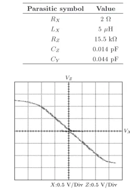
For the simulation and experimental tests, we used the CCII implemented on an IC classier circuit previously reported. The implemented CCII has both positive and negative Z outputs. Also, 1N4148 diodes are used in both simulation and experimental tests of the proposed circuit. The employed CCII has been fabricated with CMOS AMS 0.35 m process technology. The area of the CCII circuit in the classier IC is 100 m 80 m. The parasitic element values of the CCII- are given in Table 1. To show the performance of the CCII- circuit working with 1:65 V and Vbias= 0:8 V, VZ VX (or
equivalently IZ IX) and VX VY characteristics have
been extracted and the results are given in Figures 3 and 4, respectively.
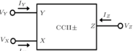
Table 1. The parasitic element values of the CCII-. Parasitic symbol Value
RX 2
LX 5 H
RZ 15.5 k
CZ 0.014 pF
CY 0.044 pF
Figure 3. VZ VX characteristics of the CCII-.
Figure 5. Experimental results for VX=VY frequency
response of the CCII-.
To obtain IZ IX characteristics, equal resistors
of 10 k are connected to X and Z terminals of the CCII-, and a DC voltage source changing from {1.5 V to 1.5 V is applied to port Y . Since X and Y scales on the oscilloscope screen are chosen as 0.5 V/Div and 0.5 V/Div, it can be realized that IZ IX
characteristics of the CCII- are operating in the range of {100 A to 125 A. A similar approach is also used to obtain VX VY characteristics of the CCII-. It can be
seen from Figure 4 that voltage VX can follow voltage
VY from {0.75 V to 1.5 V. In addition, the frequency
characteristic of the voltage gain of the CCII- is shown in Figure 5, where the test result data are collected from the measured values. f-3dB frequency of voltage gain VX=VY is 600 kHz. The important performance
parameters of the full-wave rectier circuits are the DC value transfer (pDC) and RMS error (pRMS), which are
used to show the accuracy of the rectier. These values can be respectively obtained as follows:
pDC=
R
TVoa(t)dt
R
TVoi(t)dt
; (13)
pRMS=
sR
T[VoaR(t) Voi(t)]2dt
TVoi2(t)dt ; (14)
where Voa(t) and Voi(t) represent the actual and the
ideal output values of the rectier.
In the ideal case, the values of pDC and pRMS
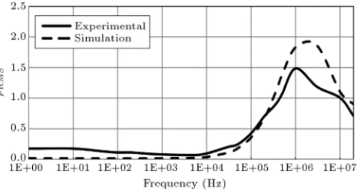
should be 1 and 0, respectively. The simulations and experimental results of pDC and pRMS are shown in
Figures 6 and 7, respectively. It can be seen that as the frequency of the full-wave rectier increases, the non-ideal eects cause the value of pDCto decrease and the
value of pRMSto increase. The time-domain simulation
result of the proposed full-wave rectier circuit is shown in Figure 8. Resistors R2= 20 k and R1= 10 k in
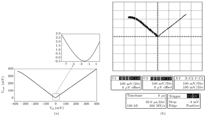
Figure 2 are chosen externally. The simulation given in Figure 8 is performed for a sinusoidal input signal with 200 mV peak value and frequency of 40 kHz. The sim-ulation and experimental results of the input-output DC transfer characteristic of the proposed full-wave
Figure 6. Simulation and experimentals result of the full-wave rectier circuit for pDC.
Figure 7. Simulation and experimental results of the full-wave rectier circuit for pRMS.
Figure 8. Time-domain response of the developed full-wave rectier.
rectier are shown in Figure 9(a) and (b), respectively. It can be seen that the circuit has a restriction on the negative input voltages approximately obtained as 370 mV from simulation and {220 mV from practical test. It should be mentioned that there is no limitation to the positive input signals since the output is directly connected to the input through resistor R2.
Nevertheless, the input-output DC transfer char-acteristic of the proposed full-wave rectier is not sym-metrical due to non-idealities of the CCII-. In addition, it can be seen from Figure 9(b) that the oset voltage is approximately zero; thus, the proposed rectier can work with very small input signals. It operates properly with input signals lower than a few mV.
The proposed full-wave rectier is also experimen-tally tested using the CCII of the classier circuit.
Figure 9. DC transfer characteristics (Vout Vin) of the suggested full-wave rectier structure: (a) simulation result, and
(b) experimental result (Y -axis = Vout, X-axis = Vin).
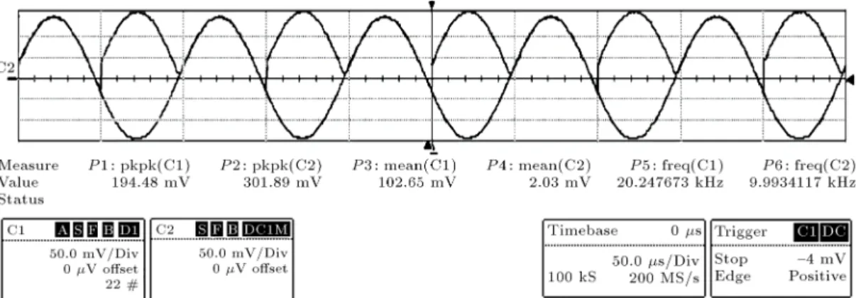
Figure 10. Input/output waveforms for input frequency of 1 kHz.
Sinusoidal voltages with frequencies of 1 kHz and 10 kHz are applied to the input of the circuit, and the rectied output signal is observed as shown in Figures 10 and 11, respectively. A comparison of the previously published rectier circuits [1-5,7-14] and the proposed one is given in Table 2.
It is observed from simulation and experimental results that they agree quite well with the claimed theory, whereas the discrepancy among them can be at-tributed to parasitics of the board used in experimental test as well as non-idealities of the CCII- and diodes. It should be mentioned that the proposed circuit has no high input and low output impedances, so buer stage may be required at its input or output. However, if the proposed circuit is used in the middle stage of
an electronic device with a low output impedance from the previous stage and high input impedance from the next stage, there is no need to use buers. Meanwhile, if necessary, a voltage buer can be easily realized by using only two MOS transistors [24].
5. Conclusion
In this paper, a new full-wave rectier circuit operating in VM is proposed. The proposed full-wave rectier circuit without requiring any external bias voltages and currents is composed of only a CCII-, two diodes, and two matched resistors. The proposed full-wave rectier structure has been designed using MENTOR software and manufactured with CMOS AMS 0.35 m
Figure 11. Input/output waveforms for input frequency of 10 kHz. Table 2. Comparison of the rectier circuits.
References [1] [2] [3] [4] [5] [7] [8] [9] [10] [11] [12] [13] [14] This work # of active
elements (# of diodes)
3 Trans-conductor 1 NMOS 1 PMOS (0)
2 CCII (2)
2 OA 1 CCII
(2) 2 OA
(2) 1 CCII
1 OA (2)
2 CCII (4)
2 CCII (4)
5 OTA (0)
1 OTA 1 NMOS
1PMOS (0)
1 CF (4)
2 CCII 3 NMOS
(0)
1 DXCCII 3 NMOS
2 CCII (2)
1 CCII-(2)
High input/ low output impedance
Yes/ No
Yes/ No
No/ Yes
No/ Yes
Yes/ Yes
Yes/ No
Yes/ No
Yes/ No
Yes/ No
No/ No
No/ No
Yes/ No
Yes/ No
No/ No # of
resistors 1 3 3 7 3 2 2 2 1 3 0 0 3 2
Resistive matching requirement
No No Yes Yes Yes Yes No No No No No No Yes Yes
Supply
voltages 5 V 1:5 V NA
NA NA 5 V NA 15 V 5 V 10 V 1:25 V 1:25 V 12 V 1:65 V NA: Not Available
technology parameters. The performances of the employed CCII- as well as the proposed full-wave rectier circuit are investigated through simulation and experimental tests which conrm the theory well as desired. Nevertheless, the dierence among the ideal, simulation, and experimental results arises from parasitics of the board used in experimental test along with non-idealities of the CCII- and diodes.
References
1. Minhaj, N. \Transconductance element-based non-inverting and non-inverting precision full-wave rectier circuits", Proc. IEEE Int. Conf. Advantages in Com-puting, Control, and Telecommunication Technologies, pp. 442-445 (2009).
2. Koton, J., Herencsar, N. and Vrba, K. \Minimal conguration versatile precision full-wave rectier us-ing current conveyors", Proc. Advances in Commu-nications Computers, Systems, Circuits and Devices, Tenerife, pp. 111-114 (2010).
3. Gift, S.J.G. \A high-performance full-wave rectier circuit", Int. Journal of Electronics, 87(8), pp. 925-930 (2000).
4. Lidgey, F.J., Haytleh K. and Toumazou, C. \New current-mode precision rectiers", Proc. IEEE Int. Symp. Circuits and Systems, pp. 1322-1325 (1993).
5. Gift, S.J.G. and Maundy, B. \Versatile precision full-wave rectiers for instrumentation and measure-ments", IEEE Trans Instrum. Meas., 56(5), pp. 1703-1710 (2007).
6. Koton, J., Herencsar, N., Vrba, K. and Minaei, S. \Pre-cision full-wave current-mode rectier using current dierencing transconductance amplier", Communica-tion Software and Networks (ICCSN), 2011 IEEE 3rd International Conference, pp. 460-463 (2011).
7. Biolek, D., Biolkova, V. and Kolka, Z. \AC analysis of operational rectiers via conventional circuit simula-tors", WSEAS Transactions on Circuits and Systems, 3(10), pp. 2291- 2295 (2004).
cur-rent conveyor precision rectier", Electronics Letters, 31(16), pp. 1302-1303 (1995).
9. Jongkunstidchai, C., Fongsamut, C., Kumwachara, K. and Surakampontorn, W. \Full-wave rectiers based on operational transconductance ampliers", Int. J. Electron. Commun., 61(3), pp. 195-201 (2007).
10. Minhaj, N. \OTA-based non-inverting and inverting precision full wave rectier circuits without diodes", Int. J. Recent Trends in Engineering, 1(3), pp. 72-75 (2009).
11. Tiliute, D.E. \Full-wave current-mode precision recti-ers using unity-gain cells", Elektronika ir Elektrotech-nika, 49(7), pp. 26-29 (2003).
12. Yuce, E., Minaei, S. and Cicekoglu, O. \Full-wave rectier realization using only two CCII+s and NMOS transistors", Int. Journal of Electron., 93(8), pp. 533-541 (2006).
13. Minaei, S. and Yuce, E. \A new full-wave rectier circuit employing single dual-X current conveyor", Int. J. Electron., 95(8), pp. 777-784 (2008).
14. Monpapassorn, A. \Low output impedance dual CCII full-wave rectier", Int. J. Electron., 100(5), pp. 648-654 (2013).
15. Kumngern, M. \New versatile precision rectier", IET Circuits Devices Syst., 8(2), pp. 141-151 (2014).
16. Koton, J., Vrba, K. and Herencsar, N. \Voltage-mode full-wave rectier based on DXCCII", Analog Integr. Circ. Sig. Process., 81, pp. 99-107 (2014).
17. Koton, J., Herencsar, N. and Vrba, K. \Precision Full-wave Rectier Using Current Conveyors and Two Diodes", ICN 2012 : The Eleventh International Conference on Networks (2012).
18. Franco, S., Design with Operational Ampliers and Analog Integrated Circuits, 2nd Edn., Mcgraw-Hill International Edition, pp. 427-429 (1998).
19. Sedra, A.S. and Smith, K.C., Microelectronics Circuits, 6th Edn., Oxford University Press, pp. 1086-1087 (2011).
20. Biolek, D., Hancioglu, E. and Keskin, A.U. \High-performance current dierencing transconductance amplier and its application in precision current-mode rectication", Int. J. Electron. Commun., 62(2), pp. 92-96 (2008).
21. Khateb, F., Vavra, J. and Biolek, D. \A novel current-mode full-wave rectier based on one CDTA and two diodes", Radioengineering, 19(3), pp. 437-445 (2010).
22. Yuce, E. and Alpaslan, H. \A CMOS current recti-er conguration suitable for integration", Journal of Circuits, Systems and Computers, 21(7), p. 1250052 (2012).
23. Minaei, S. and Yuce, E. \E. New squarer circuits and a current-mode full-wave rectier topology suitable for integration", Radioengineering, 19(4), pp. 657-661 (2010).
24. Bruun, E. \A combined rst- and second-generation current conveyor structure", International Journal of Electronics, 78(5), pp. 911-923 (1995).
Biographies
Merih Yildiz received BS and MSc degrees in Elec-tronics and Communication Engineering from Istanbul Technical University, Istanbul, Turkey, and PhD degree in Electronics Engineering from the same university in 2000, 2003, and 2009, respectively. He was a Field Support Engineer with Nortel Networks-Netas from 2000 to 2001. He is currently an Assistant Professor at the Department of Electronics and Communications Engineering, Dogus University, Istanbul, Turkey. His current research interests include current-mode circuits and analog signal processing.
Shahram Minaei received BSc degree in Electrical and Electronics Engineering from Iran University of Science and Technology, Tehran, Iran in 1993 and MSc and PhD degrees in Electronics and Communication Engineering from Istanbul Technical University, Istan-bul, Turkey in 1997 and 2001, respectively. He is currently a Professor at the Department of Electronics and Communications Engineering, Dogus University, Istanbul, Turkey. He has more than 150 publications in scientic journals or conference proceedings. His current eld of research concerns current-mode circuits and analog signal processing. Dr. Minaei is a senior member of the IEEE, an Associate Editor of the Journal of Circuits, Systems and Computers (JCSC), and an area editor of the International Journal of Electronics and Communications (AEU).
Erkan Yuce was born in 1969 in Nigde, Turkey. He received BSc degree from Middle East Technical University, MSc degree from Pamukkale University, and PhD degree from Bogazici University all in Elec-trical and Electronics Engineering in 1994, 1998, and 2006, respectively. He is currently an Associative Professor at the Electrical and Electronics Engineering Department of Pamukkale University. His current research interests include analog circuits, active lters, synthetic inductors, and CMOS-based circuits. He is the author or co-author of about 140 papers published in scientic journals or conference proceedings.