1
172234fb
TYPICAL APPLICATION
FEATURES
DESCRIPTION
Single, Dual, Quad 200MHz
Low Noise Precision Op Amps
The LT
®1722/LT1723/LT1724 are single/dual/quad, low
noise, low power, high speed operational amplifi ers. These
products feature lower input offset voltage, lower input bias
current and higher DC gain than devices with comparable
bandwidth. The 200MHz gain bandwidth ensures high
open-loop gain at video frequencies.
The low input noise voltage is achieved with reduced
supply current. The total noise is optimized for a source
resistance between 0.8k and 12k. Due to the input bias
current cancellation technique used, the resistance seen
by each input does not need to be balanced.
The output drives a 150Ω load to ±3V with ±5V supplies.
On a single 5V supply the output swings from 1.5V to
3.5V with a 500Ω load connected to 2.5V. The amplifi er
is unity-gain stable (C
LOAD
≤ 100pF).
The LT1722/LT1723/LT1724 are manufactured on Linear
Technology’s advanced low voltage complementary
bipolar process. The LT1722 is available in the SO-8 and
5-pin SOT-23 packages. The LT1723 is available in the
SO-8 and MS8 packages. The LT1724 is available in the
14-lead SO package.
Differential Video Line Driver
APPLICATIONS
n
3.8nV/√Hz Input Noise Voltage
n3.7mA Supply Current
n
200MHz Gain Bandwidth
n
Low Total Harmonic Distortion: – 85dBc at 1MHz
n70V/μs Slew Rate
n
400μV Maximum Input Offset Voltage
n300nA Maximum Input Bias Current
nUnity-Gain Stable
n
Capacitive Load Stable Up to 100pF
n23mA Minimum Output Current
nSpecifi ed at ±5V and Single 5V
n
Low Profi le (1mm) SOT-23 (ThinSot
™
) Package
n
Video and RF Amplifi cation
nADSL, HDSL II, VDSL Receivers
nActive Filters
n
Wideband Amplifi ers
nBuffers
n
Data Acquisition Systems
L, LT, LTC, LTM, Linear Technology and the Linear logo are registered trademarks of Linear Technology Corporation. ThinSOT is a trademark of Linear Technology Corporation. All other trademarks are the property of their respective owners.
Line Driver Mulitburst Video Signal
–
+
1/2 LT1723 R5 2k R3 750Ω R7 62.5Ω +VOUT VIN/2 62.5Ω LOAD 62.5Ω LOAD –VIN/2 –VIN 1723 TA01 VIN –VOUT 125Ω CAT-5 TWISTED PAIR C1 5pF–
+
1/2 LT1723 R4 2k VIN 75Ω SOURCE R22k R1 75Ω R6 62.5Ω C2 5pF +VOUT 0.5V/DIV –VOUT 0.5V/DIV VIN 1V/DIV 1723 TA022
172234fb
PIN CONFIGURATION
ABSOLUTE MAXIMUM RATINGS
Total Supply Voltage (V
+
to V
–
) ... 12.6V
Input Voltage ... ±V
S
Differential Input Voltage (Note 2) ...±0.7V
Input Current (Note 2) ... ±10mA
Output Short-Circuit Duration (Note 3) ... Indefi nite
(Note 1)
LT1722 TOP VIEW NC V+ OUT NC NC –IN +IN V– S8 PACKAGE 8-LEAD PLASTIC SO 1 2 3 4 8 7 6 5+
–
TJMAX = 150°C, θJA = 150°C/W LT1722 OUT 1 V– 2 TOP VIEW S5 PACKAGE 5-LEAD PLASTIC TSOT-23 +IN 3 5 V+ 4 –IN + – TJMAX = 150°C, θJA = 250°C/W LT1723 TOP VIEW V+ OUT B –IN B +IN B OUT A –IN A +IN A V– S8 PACKAGE 8-LEAD PLASTIC SO 1 2 3 4 8 7 6 5 A B TJMAX = 150°C, θJA = 190°C/W LT1723 1 2 3 4 OUT A –IN A +IN A V– 8 7 6 5 V+ OUT B –IN B +IN B TOP VIEW MS8 PACKAGE 8-LEAD PLASTIC MSOPA B TJMAX = 150°C, θJA = 250°C/W LT1724 TOP VIEW S PACKAGE 14-LEAD PLASTIC SO 1 2 3 4 5 6 7 14 13 12 11 10 8 8 OUT A –IN A +IN A V+ +IN B –IN B OUT B OUT D –IN D +IN D V– +IN C –IN C OUT C + – + – A D + – + –B C TJMAX = 150°C, θJA = 100°C/W
Operating Temperature Range (Note 4) ...–40°C to 85°C
Specifi ed Temperature Range (Note 5) ....–40°C to 85°C
Maximum Junction Temperature ... 150°C
Storage Temperature Range ... –65°C to 150°C
Lead Temperature (Soldering, 10 sec)... 300°C
3
172234fb
ORDER INFORMATION
LEAD FREE FINISH
TAPE AND REEL
PART MARKING*
PACKAGE DESCRIPTION
SPECIFIED
TEMPERATURE RANGE
LT1722CS8#PBF
LT1722CS8#TRPBF
1722
8-Lead Plastic SO
0°C to 70°C
LT1722IS8#PBF
LT1722IS8#TRPBF
1722I
8-Lead Plastic SO
–40°C to 85°C
LT1722CS5#PBF
LT1722CS5#TRPBF
LTZB
5-Lead Plastic TSOT-23
0°C to 70°C
LT1722IS5#PBF
LT1722IS5#TRPBF
LTZB
5-Lead Plastic TSOT-23
–40°C to 85°C
LT1723CS8#PBF
LT1723CS8#TRPBF
1723
8-Lead Plastic SO
0°C to 70°C
LT1723IS8#PBF
LT1723IS8#TRPBF
1723I
8-Lead Plastic SO
–40°C to 85°C
LT1723CMS8#PBF
LT1723CMS8#TRPBF
LTYC
8-Lead Plastic MSOP
0°C to 70°C
LT1723IMS8#PBF
LT1723IMS8#TRPBF
LTZA
8-Lead Plastic MSOP
–40°C to 85°C
LT1724CS#PBF
LT1724CS#TRPBF
LT1724CS
14-Lead Plastic SO
0°C to 70°C
LT1724IS#PBF
LT1724IS#TRPBF
LT1724IS
14-Lead Plastic SO
–40°C to 85°C
Consult LTC Marketing for parts specifi ed with wider operating temperature ranges. *The temperature grade is identifi ed by a label on the shipping container.
Consult LTC Marketing for information on non-standard lead based fi nish parts.
For more information on lead free part marking, go to:
http://www.linear.com/leadfree/
4
172234fb
ELECTRICAL CHARACTERISTICS
SYMBOL
PARAMETER
CONDITIONS
MIN
TYP
MAX
UNITS
V
OSInput Offset Voltage
(Note 6)
LT1722 SOT-23 and LT1723 MS8
100
150
400
650
μV
μV
I
OSInput Offset Current
40
300
nA
I
BInput Bias Current
40
300
nA
e
nInput Noise Voltage
f = 10kHz
3.8
nV/√
Hz
i
nInput Noise Current
f = 10kHz
1.2
pA/√
Hz
R
INInput Resistance
V
CM= ±3.5V
Differential
5
35
50
MΩ
kΩ
C
INInput Capacitance
2
pF
Input Voltage Range +
Input Voltage Range
–
3.5
4
–4
–3.5
V
V
CMRR
Common Mode Rejection Ratio
V
CM= ±3.5V
80
100
dB
PSRR
Power Supply Rejection Ratio
V
S= ±2.3V to ± 5.5V
78
90
dB
A
VOLLarge-Signal Voltage Gain
V
OUT= ±3V, R
L= 500Ω
V
OUT= ±3V, R
L= 150
Ω
10
7
17
14
V/mV
V/mV
V
OUTOutput Swing
R
L= 500Ω, V
IN= ±10mV
R
L= 150
Ω
, V
IN= ±10mV
±3.2
±3.1
±3.8
±3.4
V
V
I
OUTOutput Current
V
OUT= ± 3V, 10mV Overdrive
23
50
mA
I
SCShort-Circuit Current
V
OUT= 0V, V
IN= ±1V
35
90
mA
SR
Slew Rate
A
V= –1, (Note 7)
45
70
V/μs
Full Power Bandwidth
3V Peak, (Note 8)
3.7
MHz
GBW
Gain Bandwidth
f = 200kHz
115
200
MHz
t
SSettling Time
A
V= –1, 2V, 0.1%
A
V= –1, 2V, 0.01%
91
112
ns
ns
t
r, t
fRise Time, Fall Time
A
V= 1, 10% to 90%, V
IN= 0.2V
P-P, R
L= 150Ω
6
ns
Overshoot
A
V= 1, V
IN= 0.2V
P-P, R
L= 150Ω, R
F= 0Ω
15
%
Propagation Delay
50% V
INto 50% V
OUT= 0.2V
P-P, R
L= 150Ω
3
ns
R
OOutput Resistance
A
V= 1, f = 1MHz
0.15
Ω
Channel Separation
V
OUT= ±3V, R
L= 150Ω
82
90
dB
I
SSupply Current
Per Amplifi er
3.7
4.5
mA
T
A
= 25°C. V
S
= 5V, V
CM
= 2.5V, R
L
to 2.5V, unless otherwise noted.
V
OSInput Offset Voltage
(Note 6)
LT1722 SOT-23 and LT1723 MS8
250
350
550
800
μV
μV
I
OSInput Offset Current
20
300
nA
I
BInput Bias Current
20
300
nA
e
nInput Noise Voltage
f = 10kHz
4
nV/
√
Hz
i
nInput Noise Current
f = 10kHz
1.1
pA/
√
Hz
R
INInput Resistance
V
CM= 1.5V to 3.5V
Differential
5
32
55
MΩ
kΩ
C
INInput Capacitance
2
pF
Input Voltage Range +
Input Voltage Range –
3.5
4
1
1.5
V
V
5
172234fb
ELECTRICAL CHARACTERISTICS
T
A
= 25°C. V
S
= 5V, V
CM
= 2.5V, R
L
to 2.5V, unless otherwise noted.
SYMBOL
PARAMETER
CONDITIONS
MIN
TYP
MAX
UNITS
CMRR
Common Mode Rejection Ratio
V
CM= 1.5V to 3.5V
80
100
dB
A
VOLLarge-Signal Voltage Gain
V
OUT= 1.5V to 3.5V, R
L= 500Ω
4
10
V/mV
V
OUTOutput Swing+
Output Swing–
R
L= 500Ω, V
IN= ±10mV
R
L= 500Ω, V
IN= ±10mV
3.6
3.8
0.9
1.4
V
V
I
OUTOutput Current
V
OUT= 3.5V or 1.5V, 10mV Overdrive
10
20
mA
I
SCShort-Circuit Current
V
OUT= 2.5V, V
IN= ±1V
22
55
mA
SR
Slew Rate
A
V= –1, (Note 7)
40
70
V/µs
Full Power Bandwidth
1V Peak, (Note 8)
8.7
MHz
GBW
Gain Bandwidth (Note 10)
f = 200kHz
115
180
MHz
t
r, t
fRise Time, Fall Time
A
V= 1, 10% to 90%, V
IN= 0.2V
P-P, R
L= 500Ω
5
ns
Overshoot
A
V= 1, V
IN= 0.2V
P-P, R
L= 500Ω
16
%
Propagation Delay
50% V
INto 50% V
OUT, 0.1V, R
L= 500Ω
3
ns
R
OOutput Resistance
A
V= 1, f = 1MHz
0.19
Ω
Channel Separation
V
OUT= 1.5V to 3.5V, R
L= 500Ω
82
90
dB
I
SSupply Current
Per Amplifi er
3.8
5
mA
The
●
denotes the specifi cations which apply over the temperature range of 0°C ≤ T
A
≤ 70°C. V
S
= ±5V, V
CM
= 0V,
unless otherwise noted. (Note 5)
SYMBOL
PARAMETER
CONDITIONS
MIN
TYP
MAX
UNITS
V
OSInput Offset Voltage
(Note 6)
LT1722 SOT-23 and LT1723 MS8
l
l
700
850
μV
μV
Input V
OSDrift
(Note 9)
l
3
7
μV/°C
I
OSInput Offset Current
l
350
nA
I
BInput Bias Current
l
350
nA
Input Voltage Range +
Input Voltage Range
–
l
l
3.5
–3.5
V
V
CMRR
Common Mode Rejection Ratio
V
CM= ±3.5V
l
75
dB
PSRR
Power Supply Rejection Ratio
V
S= ±2.3V to ±5.5V
l
76
dB
A
VOLLarge-Signal Voltage Gain
V
OUT= ±3V, R
L= 500
Ω
V
OUT= ±3V, R
L= 150
Ω
l
l
9
6
V/mV
V/mV
V
OUTOutput Swing
R
L= 500Ω, V
IN= ±10mV
R
L= 150Ω, V
IN= ±10mV
l
l
±3.15
±3.05
V
V
I
OUTOutput Current
V
OUT= ±3V, 10mV Overdrive
l
22
mA
I
SCShort-Circuit Current
V
OUT= 0V, V
IN= ±1V
l
30
mA
SR
Slew Rate
A
V= –1, (Note 7)
l
35
V/μs
GBW
Gain Bandwidth
f = 200kHz
l
100
MHz
Channel Separation
V
OUT= ±3V, R
L= 150Ω
l
81
dB
6
172234fb
ELECTRICAL CHARACTERISTICS
The
l
denotes the specifi cations which apply over the temperature range of
0°C ≤ T
A
≤ 70°C. V
S
= 5V, V
CM
= 2.5V, R
L
to 2.5V, unless otherwise noted. (Note 5)
SYMBOL
PARAMETER
CONDITIONS
MIN
TYP
MAX
UNITS
V
OSInput Offset Voltage
(Note 6)
LT1722 SOT-23 and LT1723 MS8
l
l
850
950
μV
μV
Input V
OSDrift
(Note 9)
l
3
7
μV/°C
I
OSInput Offset Current
l
350
nA
I
BInput Bias Current
l
350
nA
Input Voltage Range +
Input Voltage Range
–
l
l
3.5
1.5
V
V
CMRR
Common Mode Rejection Ratio
V
CM= 1.5V to 3.5V
l
75
dB
A
VOLLarge-Signal Voltage Gain
V
OUT= 1.5V to 3.5V, R
L= 500
Ω
l
3
V/mV
V
OUTOutput Swing+
Output Swing–
R
L= 500Ω, V
IN= ±10mV
R
L= 500Ω, V
IN= ±10mV
l
l
3.55
1.45
V
V
I
OUTOutput Current
V
OUT= 3.5V, or 1.5V, 10mV Overdrive
l
9
mA
I
SCShort-Circuit Current
V
OUT= 2.5V, V
IN= ±1V
l
11
mA
SR
Slew Rate
A
V= –1, (Note 7)
l
30
V/μs
GBW
Gain Bandwidth (Note 10)
f = 200kHz
l
100
MHz
Channel Separation
V
OUT= 1.5V to 3.5V, R
L= 500Ω
l
81
dB
I
SSupply Current
l
5.95
mA
The
l
denotes the specifi cations which apply over the temperature range of –40°C ≤ T
A
≤ 85°C. V
S
= ± 5V, V
CM
= 0V,
unless otherwise noted. (Note 5)
SYMBOL
PARAMETER
CONDITIONS
MIN
TYP
MAX
UNITS
V
OSInput Offset Voltage
(Note 6)
LT1722 SOT-23 and LT1723 MS8
l
l
1100
900
μV
μV
Input V
OSDrift
(Note 9)
l
3
10
μV/°C
I
OSInput Offset Current
l
400
nA
I
BInput Bias Current
l
400
nA
Input Voltage Range +
Input Voltage Range –
l
l
3.5
–3.5
V
V
CMRR
Common Mode Rejection Ratio
V
CM= ±3.5V
l
75
dB
PSRR
Power Supply Rejection Ratio
V
S= ±2.0V to ±5.5V
l
75
dB
A
VOLLarge-Signal Voltage Gain
V
OUT= ±3V, R
L= 500Ω
V
OUT= ±3V, R
L= 150Ω
l
l
8
5
V/mV
V/mV
V
OUTOutput Swing
R
L= 500Ω, V
IN= ±10mV
R
L= 150Ω, V
IN= ±10mV
l
l
±3.1
±3.0
V
V
I
OUTOutput Current
V
OUT= ±3V, 10mV Overdrive
l
20
mA
I
SCShort-Circuit Current
V
OUT= 0V, V
IN= ±1V
l
25
mA
SR
Slew Rate
A
V= –1, (Note 7)
l
25
V/μs
GBW
Gain Bandwidth
f = 200kHz
l
90
MHz
Channel Separation
V
OUT= ±3V, R
L= 150Ω
l
80
dB
7
172234fb
ELECTRICAL CHARACTERISTICS
The
●
denotes the specifi cations which apply over the temperature range of
–40°C ≤ T
A
≤ 85°C. V
S
= 5V, V
CM
= 2.5V, R
L
to 2.5V, unless otherwise noted. (Note 5)
Note 1:
Stresses beyond those listed under Absolute Maximum Ratings
may cause permanent damage to the device. Exposure to any Absolute
Maximum Rating condition for extended periods may affect device
reliability and lifetime.
Note 2:
The inputs are protected by back-to-back diodes. If the differential
input voltage exceeds 0.7V, the input current should be limited to less than
10mA.
Note 3:
A heat sink may be required to keep the junction temperature
below the absolute maximum rating when the output is shorted
indefi nitely.
Note 4:
The LT1722C/LT1722I, LT1723C/LT1723I, LT1724C/LT1724I are
guaranteed functional over the operating temperature range of
–40°C to 85°C.
Note 5:
The LT1722C/LT1723C/LT1724C are guaranteed to meet specifi ed
performance from 0°C to 70°C. The LT1722C/LT1723C/LT1724C are
SYMBOL
PARAMETER
CONDITIONS
MIN
TYP
MAX
UNITS
V
OSInput Offset Voltage
(Note 6)
LT1722 SOT-23 and LT1723 MS8
l
l
1000
1200
µV
µV
Input V
OSDrift
(Note 9)
l
3
10
μV/°C
I
OSInput Offset Current
l
400
nA
I
BInput Bias Current
l
400
nA
Input Voltage Range +
Input Voltage Range –
l
l
3.5
1.5
V
V
CMRR
Common Mode Rejection Ratio
V
CM= 1.5V to 3.5V
l
75
dB
A
VOLLarge-Signal Voltage Gain
V
OUT= 1.5V to 3.5V, R
L= 500
Ω
l
2
V/mV
V
OUTOutput Swing+
Output Swing–
R
L= 500
Ω
, V
IN= ±10mV
R
L= 500
Ω
, V
IN= ±10mV
l
l
3.5
1.5
V
V
I
OUTOutput Current
V
OUT= 3.5V or 1.5V, 30mV Overdrive
l
8
mA
I
SCShort-Circuit Current
V
OUT= 2.5V, V
IN= ±1V
l
10
mA
SR
Slew Rate
A
V= –1, (Note 7)
l
20
V/μs
GBW
Gain Bandwidth (Note 10)
f = 200kHz
l
90
MHz
Channel Separation
V
OUT= 1.5V to 3.5V, R
L= 500
Ω
l
80
dB
I
SSupply Current
l
6.45
mA
designed, characterized and expected to meet specifi ed performance from
–40°C to 85°C but are not tested or QA sampled at these temperatures.
The LT1722I/LT1723I/LT1724I are guaranteed to meet specifi ed
performance from –40°C to 85°C.
Note 6:
Input offset voltage is pulse tested and is exclusive of warm-up
drift.
Note 7:
Slew rate is measured between ±2V on the output with ±3V input
for ±5V supplies and ±1V on the output with ±1.5V input for single 5V
supply. (For 5V supply, the voltage levels are 2.5V referred.)
Note 8:
Full power bandwidth is calculated from the slew rate:
FPBW = SR/2
π
V
PNote 9 :
This parameter is not 100% tested.
8
172234fb
TYPICAL PERFORMANCE CHARACTERISTICS
Input Bias Current
vs Temperature
Input Noise Spectral Density
Open-Loop Gain
vs Resistive Load
Total Noise
vs Unmatched Source Resistance
Warm-Up Drift vs Time
V
OS
Shift vs V
CM
and V
S
Supply Current vs Temperature
Input Common Mode Range
vs Supply Voltage
Input Bias Current
vs Common Mode Voltage
TEMPERATURE (°C) –50 SUPPL Y CURRENT (mA) 4.0 4.5 5.0 25 75 1723 G01 3.5 3.0 –25 0 50 100 125 2.5 2.0 PER AMPLIFIER VS = 5V VS = ±5V SUPPLY VOLTAGE (±V) 0
INPUT COMMON MODE RANGE (V)
2 4 5 1723 G02 1 3 6 7 0.5 V+ –0.5 –1.0 –1.5 –1.2 2.0 1.5 1.0 0.5 V– (VOS) < 500μV TA = 25°C
INPUT COMMON MODE VOLTAGE (V) –5
INPUT BIAS CURRENT (nA)
400 300 200 100 0 –100 –200 –300 –400 3 1723 G03 –3 –1 1 2 5 –4 –2 0 4 VS = ±5V TA = –45°C TA = 125°C TA = 25°C TA = 85°C TEMPERATURE (°C) –50
INPUT BIAS CURRENT (nA)
20 40 60 25 75 1723 G04 0 –20 –25 0 50 IB– IB– IB+ IB+ 100 125 –40 –60 VS = ±5V VS = 5V FREQUENCY (kHz) 0.01 0.1 1 10 100 0.1 1 10 in 1 10 100 1723 G05
INPUT VOLTAGE NOISE (nV/√
Hz
) INPUT CURRENT NOISE (pA/√
Hz ) en LOAD RESISTANCE (Ω) 100 74.0 OPEN-LOOP GAIN (dB) 76.5 79.0 81.5 84.0 89.0 1000 10000 1723 G06 86.5 TA = 25°C VS = ±5V, VO = ±3V VS = ±2.5V, VO = ±1V SOURCE RESISTANCE, RS (kΩ) 1
TOTAL NOISE VOLTAGE (nV/√
Hz ) 10 0.01 1 10 100 1723 G07 0.1 0.1 100 VS = ±5V TA = 25°C f = 10kHz TOTAL NOISE RESISTOR NOISE
+
–
RSTIME AFTER POWER-UP (SEC) 0
OFFSET VOLTAGE DRIFT (μV)
10 20 30 5 15 25 20 40 60 80 1723 G08 100 10 0 30 50 70 90 LT1722S8 TA = 25°C TYPICAL DATA VS = ±5V VS = ±2.5V
COMMON MODE VOLTAGE (V) –300 VOS SHIFT (μV) –100 100 300 –200 0 200 –3 –1 1 3 1723 G09 5 –4 –5 –2 0 2 4 VS = ±6.3V VS = ±5V VS = ±4V VS = ±3V VS = ±2.5V TA = 25°C TYPICAL PART VS = ±6V
9
172234fb
TYPICAL PERFORMANCE CHARACTERISTICS
Open-Loop Gain vs Temperature
Output Voltage Swing
vs Supply Voltage
Output Short-Circuit Current
vs Temperature
Gain and Phase vs Frequency
Overshoot vs Capacitive Load
Output Impedance vs Frequency
V
OS
vs Temperature
Undistorted Output Swing
vs Frequency
Undistorted Output Swing
vs Frequency
TEMPERATURE (°C) –60 –500 OFFSET VOLTAGE (μV) –400 –200 –100 0 60 80 100 200 1723 G10 –300 –40 –20 0 20 40 120 100 VS = ±5V TYPICAL PART VS = ±2.5V FREQUENCY (MHz) 0.1 0 OUTPUT VOLTAGE (V P-P ) 2 4 6 8 1 10 1723 G11 10 1 3 5 7 9 AV = 1, RF = 0Ω, RIN = 500Ω AV = –1, RF = 500Ω VS = ±5V RL = 150Ω 2% MAX DISTORTION FREQUENCY (MHz) 0.1 0 OUTPUT VOLTAGE (V P-P ) 1.0 2.0 3.0 4.0 1 10 1723 G12 5.0 0.5 1.5 2.5 3.5 4.5 AV = –1, RF = 500Ω VS = 5V RL = 500Ω 2% MAX DISTORTION AV = 1, RF = 0Ω, RIN = 500Ω TEMPERATURE (°C) –50 86 OPEN-LOOP GAIN (dB) 76 78 79 80 85 82 0 50 75 1723 G13 77 83 84 81 –25 25 100 125 VS = ±5V, VO = ±3V VS = 5V, VO = ±1V RL = 500Ω RL = 500Ω RL = 150Ω SUPPLY VOLTAGE (±V) 2.0OUTPUT VOLTAGE SWING (V)
2.5 3.0 3.5 4.0 4.5 5.0 1723 G08 5.5 V+ –0.5 –1.0 –1.5 –2.0 2.0 1.5 1.0 0.5 V– 6.0 TA = 25°C VIN = 10mV RL = 500Ω RL = 500Ω RL = 150Ω RL = 150Ω TEMPERATURE (°C) –50 60
OUTPUT SHORT-CIRCIUT CURRENT (mA) 65
75 80 85 110 95 0 50 75 1723 G15 70 100 105 90 –25 25 100 125 VS = ±5V VS = 5V SOURCE SOURCE SINK SINK FREQUENCY (MHz) 20 GAIN (dB) PHASE (DEG) 80 90 10 0 70 40 60 50 30 0.01 1 10 100 1723 G16 –10 20 80 90 10 0 70 40 60 50 30 –10 0.1 PHASE GAIN ±5V ±5V 5V 5V TA = 25°C AV = –1 RF = RG = 500Ω CAPACITIVE LOAD (pF) 10 OVERSHOOT (%) 50 60 70 80 50 1723 G17 40 30 45 55 65 75 35 25 20 20 30 40 60 70 80 90 100 VS = ±5V RL = 500Ω VIN = 2VP-P f = 1MHz AV = –1, RF = 500Ω, RS = 0Ω AV = 1, RF = 0Ω, RS = 500Ω AV = 1, RF = 500Ω, RS = 0Ω FREQUENCY (MHz) 0.010.001 OUTPUT IMPEDANCE (Ω) 0.1 100 1 10 0.1 100 1723 G18 0.01 1 10 TA = 25°C VS = ±5V AV = 100 AV = 10 AV = 1
10
172234fb
TYPICAL PERFORMANCE CHARACTERISTICS
Channel Separation vs Frequency
Power Supply Rejection Ratio
vs Frequency
Common Mode Rejection Ratio
vs Frequency
Slew Rate vs Temperature
Phase Margin vs Supply Voltage
Gain Bandwidth
vs Supply Voltage
Gain vs Frequency, A
V
= 1
Gain vs Frequency, A
V
= 1
Gain vs Frequency, A
V
= –1
FREQUENCY (MHz) 1 –1 GAIN (dB) 1 3 5 7 10 100 1723 G19 0 2 4 6 8 9 TA = 25°C AV = 1 RF = 0Ω NO RL ±5V 5V CL = 100pF CL = 50pF CL = 0pF FREQUENCY (MHz) 1 –1 GAIN (dB) 1 3 5 7 10 100 1723 G20 0 2 4 6 8 9 TA = 25°C AV = 1 NO RL NO CL ±5V 5V RF = 500Ω RF = 1k RF = 0Ω FREQUENCY (MHz) 1 –1 GAIN (dB) 1 3 5 7 10 100 1723 G21 0 2 4 6 8 9 TA = 25°C AV = –1 RF = RG = 500Ω NO RL ±5V 5V CL = 100pF CL = 50pF CL = 0pF FREQUENCY (MHz) 0.1 –50 CROSSTALK (dB) –30 –10 1 10 100 1723 G22 –70 –60 –40 –20 –80 –90 TA = 25°C VO = 6VP-P RL = 150Ω FREQUENCY (MHz) 40
POWER SUPPLY REJECTION RATIO (dB)
100 30 20 90 60 80 70 50 0.01 1 10 100 1723 G23 10 0 0.1 TA = 25°C VS = ±5V AV = 1 –PSRR +PSRR FREQUENCY (MHz) 40
COMMON MODE REJECTION RATIO (dB)
100 110 30 20 90 60 80 70 50 0.01 1 10 100 1723 G24 10 0.1 TA = 25°C VS = ±5V TEMPERATURE (°C) –50 SLEW RATE (V/μs) 90 25 1723 G40 60 40 –25 0 50 30 20 100 80 70 50 75 100 125 TA = 25°C AV = –1 RG = RF = 500Ω VS = ±5V, SR+ VS = ±5V, SR– VS = ±2.5V, SR– VS = ±2.5V, SR+ SUPPLY VOLTAGE (±V) 2.5 35
PHASE MARGIN (DEG)
40 50 55 60 4.5 80 1723 G41 45 3.5 3 4 5 5.5 6 65 70 75 TA = 25°C AV = –1 VIN = –20dBm RG = RF = 500Ω RL = 500Ω CL = 5pF CL = 25pF CL = 55pF RL = 500Ω RL = 500Ω RL = 150Ω RL = 150Ω RL = 150Ω SUPPLY VOLTAGE (±V) 2.5 GAIN BANDWIDTH (MHz) 215 4 1723 G42 200 190 3 3.5 4.5 185 180 220 210 205 195 5 5.5 6 TA = 25°C AV = –1 VIN = –20dBm RG = RF = 500Ω CL = 25pF CL = 25pF RL = 150Ω RL = 500Ω CL = 5pF CL = 5pF CL = 55pF CL = 55pF
11
172234fb
TYPICAL PERFORMANCE CHARACTERISTICS
Harmonic Distortion vs Frequency
A
V
= 2, V
O
= 0.2V
P-P
Harmonic Distortion vs Frequency
A
V
= 2, V
O
= 0.2V
P-P
Harmonic Distortion vs Frequency
A
V
= 1, V
O
= 2V
P-P
Harmonic Distortion vs Frequency
A
V
= 1, V
O
= 2V
P-P
Harmonic Distortion vs Frequency
A
V
= 2, V
O
= 2V
P-P
Slew Rate vs Supply Voltage
Harmonic Distortion vs Frequency
A
V
= 1, V
O
= 0.2V
P-P
Harmonic Distortion vs Frequency
A
V
= 1, V
O
= 0.2V
P-P
SUPPLY VOLTAGE (±V) 2 50 SLEW RATE (V/μs) 55 65 70 SR+ SR+ SR– SR– 75 3 4 4.5 6.5 1723 G25 60 2.5 3.5 5 5.5 6 80 VIN_P-P = VS, VOUT_MES AT 2/3 OF VIN_P-P VIN = ±1.5V, VOUT_MES AT ±1V TA = 25°C AV = –1 RF = RG = RL = 500Ω FREQUENCY (MHz) 0.1 –100 HARMONIC DISTORTION (dBc) –90 –80 –70 –60 –40 1 10 1723 G26 –50 VS = ±5V AV = 1 RF = 0Ω RIN = 0Ω VO = 0.2VP-P RL = 150Ω, 2ND RL = 500Ω, 2ND RL = 500Ω, 3RD RL = 150Ω, 3RD FREQUENCY (MHz) 0.1 –100 HARMONIC DISTORTION (dBc) –90 –80 –70 –60 –40 1 10 1723 G27 –50 VS = 5V AV = 1 RF = 0Ω RIN = 0Ω VO = 0.2VP-P RL = 150Ω, 2ND RL = 500Ω, 2ND RL = 150Ω, 3RD RL = 500Ω, 3RD FREQUENCY (MHz) 0.1 –100 HARMONIC DISTORTION (dBc) –90 –80 –70 –60 –40 1 10 1723 G28 –50 VS = ±5V AV = 2 RF = 500Ω VO = 0.2VP-P RL = 150Ω, 2ND RL = 150Ω, 3RD RL = 500Ω, 2ND RL = 500Ω, 3RD FREQUENCY (MHz) 0.1 –100 HARMONIC DISTORTION (dBc) –90 –80 –70 –60 –40 1 10 1723 G29 –50 VS = 5V AV = 2 RF = 500Ω VO = 0.2VP-P RL = 150Ω, 2ND RL = 150Ω, 3RD RL = 500Ω, 2ND RL = 500Ω, 3RD FREQUENCY (MHz) 0.1 –100 HARMONIC DISTORTION (dBc) –90 –80 –70 –60 –40 1 10 1723 G30 –50 VS = ±5V AV = 1 RF = 0Ω RIN = 500Ω VO = 2VP-P RL = 150Ω, 3RD RL = 500Ω, 3RD RL = 150Ω, 2ND RL = 500Ω, 2ND FREQUENCY (MHz) 0.1 –100 HARMONIC DISTORTION (dBc) –90 –80 –70 –60 –40 1 10 1723 G31 –50 VS = 5V AV = 1 RF = 0Ω RIN = 500Ω VO = 2VP-P RL = 150Ω, 3RD RL = 500Ω, 3RD RL = 150Ω, 2ND RL = 500Ω, 2ND FREQUENCY (MHz) 0.1 –100 HARMONIC DISTORTION (dBc) –90 –80 –70 –60 –40 1 10 1723 G32 –50 VS = ±5V AV = 2 RF = 500Ω VO = 2VP-P RL = 150Ω, 3RD RL = 500Ω, 3RD RL = 500Ω, 2ND RL = 150Ω, 2ND12
172234fb
TYPICAL PERFORMANCE CHARACTERISTICS
Large-Signal Transient, A
V
= 1
Small-Signal Transient, A
V
= 1
Small-Signal Transient, A
V
= 1
Large-Signal Transient, A
V
= –1
Small-Signal Transient, A
V
= –1
Harmonic Distortion vs Frequency
A
V
= 2, V
O
= 2V
P-P
Settling Time vs Output Step
FREQUENCY (MHz) 0.1 –100 HARMONIC DISTORTION (dBc) –90 –80 –70 –60 –40 1 10 1723 G33 –50 VS = 5V AV = 2 RF = 500Ω VO = 2VP-P RL = 150Ω, 3RD RL = 500Ω, 3RD RL = 500Ω, 2ND RL = 150Ω, 2ND SETTLING TIME (ns) 60 OUTPUT STEP (V) 0 1.5 2.0 140 1723 G43 –0.5 –1.0 –3.0 80 100 120 70 90 110 130 –2.0 3.0 2.5 1.0 0.5 –1.5 –2.5 VS = ±5V AV = –1 RF = 500Ω CF = 0pF 0.1% SETTLING 0.1% SETTLING 0.01% SETTLING 0.01% SETTLING
Small-Signal Transient, A
V
= –1
1V/DIV AV = 1 RS = 500Ω RF = 0Ω 50ns/DIV 1723 G34 50mV/DIV AV = 1 RS = 0Ω RF = 0Ω CL = 0pF 50ns/DIV 1723 G35 50mV/DIV AV = 1 RS = 0Ω RF = 0Ω CL = 100pF 50ns/DIV 1723 G36 1V/DIV AV = –1 RG = 500Ω RF = 500Ω 50ns/DIV 1723 G37 50mV/DIV AV = –1 RG = 500Ω RF = 500Ω CL = 0pF 50ns/DIV 1723 G38 50mV/DIV AV = –1 RG = 500Ω RF = 500Ω CL = 100pF 50ns/DIV 1723 G3913
172234fb
The LT1722/LT1723/LT1724 may be inserted directly into
many operational amplifi er applications improving both DC
and AC performance, as well as noise and distortion.
Layout and Passive Components
The LT1722/LT1723/LT1724 amplifi ers are more tolerant
of less than ideal layouts than other high speed amplifi ers.
For maximum performance (for example, fast settling time)
use a ground plane, short lead lengths and RF quality
bypass capacitors (0.01μF to 0.1μF). For high drive current
applications, use low ESR supply bypass capacitors (1μF
to 10μF tantalum). The output/input parasitic coupling
should be minimized when high frequency performance
is required.
The parallel combination of the feedback resistor and gain
setting resistor on the inverting input combine with the
input capacitance to form a pole that can cause peaking
or even oscillations. In parallel with the feedback resistor,
a capacitor of value:
C
F
> R
G
• C
IN
/R
F
should be used to cancel the input pole and optimize
dynamic performance. For unity-gain applications where
a feedback resistor is used, such as an I-to-V converter,
C
F
should be fi ve times greater than C
IN
; an optimum
value for C
F
is 10pF.
Input Considerations
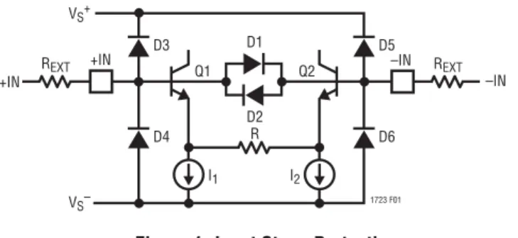
Each of the LT1722/LT1723/LT1724 inputs is protected with
back-to-back diodes across the bases of the NPN input
devices. If greater than 0.7V differential input voltages are
anticipated, the input current must be limited to less than
10mA with an external series resistor. Each input also has
two ESD clamp diodes—one to each supply. If an input is
driven beyond the supply, limit the current with an external
resistor to less than 10mA. The input stage protection
circuit is shown in Figure 1.
The input currents of the LT1722/LT1723/LT1724 are
typically in the tens of nA range due to the bias current
cancellation technique used at the input. As the input
offset current can be greater than either input current,
APPLICATIONS INFORMATION
Figure 1. Input Stage Protection
adding resistance to balance source resistance is not
recommended. The value of the source resistor should
be below 12k as it actually degrades DC accuracy and
also increases noise.
Total Input Noise
The total input noise of the LT1722/LT1723/LT1724 is
optimized for a source resistance between 0.8k and 12k.
Within this range, the total input noise is dominated by
the noise of the source resistance itself. When the source
resistance is below 0.8k, voltage noise of the amplifi er
dominates. When the source resistance is above 12k, the
input noise current is the dominant contributor.
Capacitive Loading
The LT1722/LT1723/LT1724 drive capacitive loads up to
100pF with unity gain. As the capacitive load increases,
both the bandwidth and the phase margin decrease causing
peaking in the frequency response and overshoot in the
transient response. When there is a need to drive a larger
capacitive load, a 25Ω series resistance assures stability
with any value of load capacitor. A feedback capacitor also
helps to reduce any peaking.
Power Dissipation
The LT1722/LT1723/LT1724 combine high speed and
large output drive in a small package. Maximum junction
temperature (T
J
) is calculated from the ambient temperature
(T
A
), power dissipation per amplifi er (P
D
) and number of
amplifi ers (n) as follows:
T
J
= T
A
+ (n • P
D
•
θ
JA
)
D1 D3 +IN +IN D4 D5 D6 1723 F01 D2 I1 I2 R Q1 REXT Q2 VS+ VS– –IN –IN REXT14
172234fb
SIMPLIFIED SCHEMATIC
APPLICATIONS INFORMATION
Power dissipation is composed of two parts. The fi rst is
due to the quiescent supply current and the second is due
to on-chip dissipation caused by the load current.
Worst-case instantaneous power dissipation for a given
resistive load in one amplifi er occurs at the maximum
supply current and when the output voltage is at half of
either supply voltage (or the maximum swing if less than
half supply voltage).
Therefore P
D(MAX)
in one amplifi er is:
P
D(MAX)
= (V
+
– V
–
)(I
S(MAX)
) + (V
+
/2)
2
/R
L
or
P
D(MAX)
= (V
+
– V
–
)(I
S(MAX)
) +
(V
+
– V
O(MAX)
)(V
O(MAX)
/R
L
)
Example. Worst-case conditions are: both op amps in
the LT1723IS8 are at T
A
= 85°C, V
S
= ±5V, R
L
= 150Ω,
V
OUT
= 2.5V.
P
D(MAX)
= 2 •[(10V)(5.95mA) + (2.5V)
2
/150Ω] = 203mW
T
J(MAX)
= 85°C + (203mW)(190°C/W) = 124°C
which is less than the absolute maximum rating at 150°C.
Circuit Operation
The LT1722/LT1723/LT1724 circuit topology is a voltage
feedback amplifi er. The operation of the circuit can be
understood by referring to the Simplifi ed Schematic. The
fi rst stage is a folded cascode formed by the transistors
Q1 through Q4. A degeneration resistor, R, is used in the
input stage. The current mirror Q5, Q6 is bootstrapped
by Q7. The capacitor, C, assures the bandwidth and the
slew rate performance. The output stage is formed by
complementary emitter followers, Q8 through Q11. The
diodes D1 and D2 protect against input reversed biasing.
The remaining part of the circuit assures optimum voltage
and current biases for all stages.
Low noise, reduced current supply, high speed and
DC accurate parameters are distinctive features of the
LT1722/LT1723/LT1724.
Q2 +IN Q1 D1 D2 R ?–IN R2 Q6 Q7 Q9 Q10 VS+ VS– OUT 1723 SS Q11 Q8 Q4 C VBIAS I3 I4 I5 I2 I1 R1 Q5 Q315
172234fbPACKAGE DESCRIPTION
1.50 – 1.75 (NOTE 4) 2.80 BSC 0.30 – 0.45 TYP 5 PLCS (NOTE 3) DATUM ‘A’ 0.09 – 0.20(NOTE 3) S5 TSOT-23 0302 REV B
PIN ONE 2.90 BSC (NOTE 4) 0.95 BSC 1.90 BSC 0.80 – 0.90 1.00 MAX 0.01 – 0.10 0.20 BSC 0.30 – 0.50 REF NOTE:
1. DIMENSIONS ARE IN MILLIMETERS 2. DRAWING NOT TO SCALE
3. DIMENSIONS ARE INCLUSIVE OF PLATING
4. DIMENSIONS ARE EXCLUSIVE OF MOLD FLASH AND METAL BURR 5. MOLD FLASH SHALL NOT EXCEED 0.254mm
6. JEDEC PACKAGE REFERENCE IS MO-193 3.85 MAX
0.62 MAX
0.95 REF
RECOMMENDED SOLDER PAD LAYOUT PER IPC CALCULATOR
1.4 MIN 2.62 REF
1.22 REF
S5 Package
5-Lead Plastic TSOT-23
16
172234fb
MS8 Package
8-Lead Plastic MSOP
(Reference LTC DWG # 05-08-1660 Rev F)
MSOP (MS8) 0307 REV F 0.53 ± 0.152 (.021 ± .006) SEATING PLANE NOTE: 1. DIMENSIONS IN MILLIMETER/(INCH) 2. DRAWING NOT TO SCALE3. DIMENSION DOES NOT INCLUDE MOLD FLASH, PROTRUSIONS OR GATE BURRS.
MOLD FLASH, PROTRUSIONS OR GATE BURRS SHALL NOT EXCEED 0.152mm (.006") PER SIDE 4. DIMENSION DOES NOT INCLUDE INTERLEAD FLASH OR PROTRUSIONS.
INTERLEAD FLASH OR PROTRUSIONS SHALL NOT EXCEED 0.152mm (.006") PER SIDE 5. LEAD COPLANARITY (BOTTOM OF LEADS AFTER FORMING) SHALL BE 0.102mm (.004") MAX
0.18 (.007) 0.254 (.010) 1.10 (.043) MAX 0.22 – 0.38 (.009 – .015) TYP 0.1016 ± 0.0508 (.004 ± .002) 0.86 (.034) REF 0.65 (.0256) BSC 0° – 6° TYP DETAIL “A” DETAIL “A” GAUGE PLANE 1 2 3 4 4.90 ± 0.152 (.193 ± .006) 8 7 6 5 3.00 ± 0.102 (.118 ± .004) (NOTE 3) 3.00 ± 0.102 (.118 ± .004) (NOTE 4) 0.52 (.0205) REF 5.23 (.206) MIN 3.20 – 3.45 (.126 – .136) 0.889 ± 0.127 (.035 ± .005)
RECOMMENDED SOLDER PAD LAYOUT 0.42 ± 0.038 (.0165 ± .0015) TYP 0.65 (.0256) BSC
S8 Package
8-Lead Plastic Small Outline (Narrow .150 Inch)
(Reference LTC DWG # 05-08-1610)
.016 – .050 (0.406 – 1.270) .010 – .020 (0.254 – 0.508)s 45° 0°– 8° TYP .008 – .010 (0.203 – 0.254) SO8 0303 .053 – .069 (1.346 – 1.752) .014 – .019 (0.355 – 0.483) TYP .004 – .010 (0.101 – 0.254) .050 (1.270) BSC 1 2 3 4 .150 – .157 (3.810 – 3.988) NOTE 3 8 7 6 5 .189 – .197 (4.801 – 5.004) NOTE 3 .228 – .244 (5.791 – 6.197) .245 MIN .160 ±.005RECOMMENDED SOLDER PAD LAYOUT .045 ±.005 .050 BSC .030 ±.005 TYP INCHES (MILLIMETERS) NOTE: 1. DIMENSIONS IN 2. DRAWING NOT TO SCALE
3. THESE DIMENSIONS DO NOT INCLUDE MOLD FLASH OR PROTRUSIONS. MOLD FLASH OR PROTRUSIONS SHALL NOT EXCEED .006" (0.15mm)
17
172234fb
Information furnished by Linear Technology Corporation is believed to be accurate and reliable. However, no responsibility is assumed for its use. Linear Technology Corporation makes no representa-tion that the interconnecrepresenta-tion of its circuits as described herein will not infringe on existing patent rights.
PACKAGE DESCRIPTION
S Package
14-Lead Plastic Small Outline (Narrow .150 Inch)
(Reference LTC DWG # 05-08-1610)
1 N 2 3 4 .150 – .157 (3.810 – 3.988) NOTE 3 14 13 .337 – .344 (8.560 – 8.738) NOTE 3 .228 – .244 (5.791 – 6.197) 12 11 10 9 5 6 7 N/2 8 .016 – .050 (0.406 – 1.270) .010 – .020 (0.254 – 0.508)s 45° 0° – 8° TYP .008 – .010 (0.203 – 0.254) S14 0502 .053 – .069 (1.346 – 1.752) .014 – .019 (0.355 – 0.483) TYP .004 – .010 (0.101 – 0.254) .050 (1.270) BSC .245 MIN N 1 2 3 N/2 .160 ±.005RECOMMENDED SOLDER PAD LAYOUT .045 ±.005 .050 BSC .030 ±.005 TYP INCHES (MILLIMETERS) NOTE: 1. DIMENSIONS IN 2. DRAWING NOT TO SCALE
3. THESE DIMENSIONS DO NOT INCLUDE MOLD FLASH OR PROTRUSIONS. MOLD FLASH OR PROTRUSIONS SHALL NOT EXCEED .006" (0.15mm)
18
172234fb
Linear Technology Corporation
1630 McCarthy Blvd., Milpitas, CA 95035-7417
(408) 432-1900
●FAX: (408) 434-0507
●www.linear.com
© LINEAR TECHNOLOGY CORPORATION 2002LT 0909 REV B • PRINTED IN USA
RELATED PARTS
TYPICAL APPLICATION
PART NUMBER
DESCRIPTION
COMMENTS
LT1677
Single, Low Noise Rail-to-Rail Amplifi er
3V Operation, 2.5mA Supply Current, 4.5nV/
√
Hz Max e
n,
60µV Max V
OSLT1800/LT1801/LT1802
Single/Dual/Quad, Low Power, 80MHz Rail-to-Rail
Precision Amplifi er
1.6mA Supply Current, 350µV V
OS, 2.3V Operation
LT1806/LT1807
Single/Dual, Low Noise 325MHz Rail-to-Rail Amplifi ers
2.5V Operation, 550µV
MAXV
OS, 3.5nV/
√
Hz
LT1809/LT1810
Single/Dual, Low Distortion 180MHz Rail-to-Rail Amplifi ers
2.5V Operation, –90dBc at 5MHz Distortion
LT1812/LT1813/LT1814
Single/Dual/Quad, 3mA, 750V/µs Amplifi ers
5V Operation, 3.6mA Supply Current, 40mA Min Output Current
LT6202/LT6203/LT6204
Single/Dual/Quad, 100MHz, Low Noise Rail-to-Rail Op Amps
2nV/
√
Hz, 2.5mA on Single 3V Supply
4- to 2-Wire Local Echo Cancellation Differential Receiver Amplifi er
n:1