ISSN(Online): 2319-8753 ISSN (Print) : 2347-6710
I
nternational
J
ournal of
I
nnovative
R
esearch in
S
cience,
E
ngineering and
T
echnology
(An ISO 3297: 2007 Certified Organization)
Vol. 5, Issue 6, June 2016
Study and Implementation of SPI (Serial
peripheral Interface) using VHDL and its
synthesis using Xilinx
Prakriti Porwal
Student, Department of Electronics and Communication, Indira Gandhi Delhi Technical University for Women Delhi,
India1
ABSTRACT: Serial Peripheral Protocol, it is simple protocol which allows data transfer between IC and peripheral devices at low or medium speed, communication is in full duplex mode. Thou there are many serial interfaces such as RS232, IC etc. as SPI offers more flexibility, low cost and stability it is preferred over other communication protocol. This paper includes great dealing in the study of Serial Peripheral Protocol, its simulation and synthesis using Xilinx ISE 14.1 version. The purpose is to generate the efficient coding for implementation of SPI Master Protocol.
The RTL code is implemented in VHDL and the design code is simulated in Modelsim Se Plus 5.5c while its synthesis is verified using Xilinx ISE 14.1 version for Virtex 4 and Spartan 3 FPGA devices. Synthesis provide timing analysis and substantial area overhead.
KEYWORDS: (SPI) Serial Peripheral Interface, Master, VHDL, Xilinx.
I. INTRODUCTION
SPI as a circuit technique is first proposed by Motorola Company in 1970 in its first 68000-based MCU and later it is adopted by other industry also. Simplicity of interfacing and the speed of SPI allows transferring or communication of data easily hence making it popular communication protocol.A serial peripheral interface (SPI) is an interface which allows the serial transfer of data that is one bit at a time between two devices, where one acts as master and the other acts as slave.
SPI works in two different modes:
Master Mode: In this mode the clock signal is generated by master which is known as SCK or Serial clock.
Slave Mode: The other mode is known as Slave which follows master clock
Four kind of signals is initiated by SPI Master Protocol such as:
SCK: It represents the clock signal which is controlled by Master.
MOSI (Master out Slave In): It represents the data line where, data is sent from master to the slave.
MISO (Master in Slave Out): This data line represents the response of slave back to the master after receiving or sending the data, where the master will generate the number of clock cycles, and the data will be put by slave onto data line. Since clock signal will always be generated by master, therefore whenever slave needs to return the data and how much data will be returned must be known in advance.
ISSN(Online): 2319-8753 ISSN (Print) : 2347-6710
I
nternational
J
ournal of
I
nnovative
R
esearch in
S
cience,
E
ngineering and
T
echnology
(An ISO 3297: 2007 Certified Organization)
Vol. 5, Issue 6, June 2016
Activating the slave when the data line is held low and initiate sending of data after this the line is made high. This logic is active low used to enable or reset the lines
.
FIGURE 1:SIGNALS IN SPIMASTER SLAVE PROTOCOL
SPI is so popular because of its simplicity, the hardware can be a simple shift register. This is a much simpler and cheaper than the full-up UART (Universal asynchronous Receiver / Transmitter) that asynchronous serial requires.
There are three types of data format to transfer data from master to slave device as represented in table below:
TABLE 1:FORMATS USED IN SPIPROTOCOL
Features of SPI that allows it to widely used are:
Mode of communication is full duplex and synchronous.
Throughput is higher i.e. transfer rate is defined as n*MHz to 10 n*MHz.
Bit transfer is not limited to 8 bits.
Hardware interfacing is simple.
Message size can be arbitrary, contents and purpose.
Low power requirements.
Slave is followed by master’s clock which does not require any precision oscillators. Slave can be vary from 1 to n numbers.
Less circuitry leads to lower power requirements.
II. RELATED WORK
In other work SPI is compared with other protocol for data transfer.In this paper we aim to study the Serial Peripheral Interface which is easy protocol for data transmission for low or medium communication system.
Implementing of Master SPI through efficient VHDL code.
Simulation using Modelsim SE 5c where we study the system clock and clock defined by master.
Control 0 1 2 3 4 5 6 7
SPIE SPE DORDE MSTR CPOL CPHA SPR1 SPR0
Status 8 9 10 11 12 13 14 15
SPIF WCOL - - - SPIX2
DATA 16 17 18 19 20 21 22 23
ISSN(Online): 2319-8753 ISSN (Print) : 2347-6710
I
nternational
J
ournal of
I
nnovative
R
esearch in
S
cience,
E
ngineering and
T
echnology
(An ISO 3297: 2007 Certified Organization)
Vol. 5, Issue 6, June 2016
Synthesis using Xilinx14.1, where we analyse the timing report and area of utilization for FPGA high speed devices.
III. EXPERIMENTAL RESULTS
The study of SPI Master its implementation and synthesis using VHDL is successfully done. The design code is technology independent and is stimulated at both RTL and gate level (post place and route netlist) and mapped onto Xilinx’s FPGA using Xilinx ISE 14.1 version. Both the SPI slave and master has undergone functional software verification.
FIGURE 2:TRANSACTION OF SPIMASTER USING MODELSIM
In the above figure SPI master shows the transaction of two bit data .It define four slave devices ,first slave is selected for data transfer at SS is low. At CPOL=0, SCK is low and at CPOL=1, SCK is high. When CPHA=0 it implements write operation that is data is written on second edge of the clock (SCK).When CPHA=1 it implements read operation that is data is read at first edge of clock (SCK).
ISSN(Online): 2319-8753 ISSN (Print) : 2347-6710
I
nternational
J
ournal of
I
nnovative
R
esearch in
S
cience,
E
ngineering and
T
echnology
(An ISO 3297: 2007 Certified Organization)
Vol. 5, Issue 6, June 2016
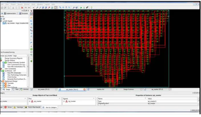
The figure 3 shows the port description for master configuration which is defined while coding and same is synthesis in Xilinx.
FIGURE 1:RTL VIEW OF MASTER DEVICE
Figure 4 shows the architectural or RTL view of master SPI.While analysing the architectural view we conclude that it consists of 119 D flip flop,6 adders and substractor,8 comparator,33 multiplexer, this defines the area utilization of high speed FPGA devices.
TABLE 2:UTILIZATION RATIO OF FPGADEVICES.
Device Utilization Summary
Device:3s50tq144-5 Device:4vfx12sf363-12
Number of slices 118 out of 786 125 out of 5427
Number of Slice Flip Flop 118 out of 1536 118 out of 10944
Number of 4 input LUTs 197 out of 1536 217 out of 10944
Number of IOs 82 82
Number of bonded IOBs 82 out of 97 82 out of 240
Number of GCLKs 1 out of 8 1 out of 32
ISSN(Online): 2319-8753 ISSN (Print) : 2347-6710
I
nternational
J
ournal of
I
nnovative
R
esearch in
S
cience,
E
ngineering and
T
echnology
(An ISO 3297: 2007 Certified Organization)
Vol. 5, Issue 6, June 2016
For instance if we consider the Clock to Setup delay of SPI master onto Vertix-4 device (3.702 ns), a transfer rate of more than 14ns can be achieved, which results to 72 Mbps.
IV. CONCLUSION
A practical study of SPI protocols has been presented. The thesis shows the result of an FPGA implementation for master side of SPI protocol.
SPI Data Rate: fclock /2*clk_div,
It defines the relative speed at which current transaction occurs, If clk_div=1 then SCLK=1/2 fclock. A maximum transfer rate 72 Mbps for master respectively. An area overhead of is 15% for Virtex 4 FPGA. An RTL code is technology independent much efficient therefore obtaining much faster transfer rate. In the work we are more focused on SPI features and its efficient implementation with maximum transfer rate and minimum area overhead. Here all the modules are designed and stimulated with VHDL .Then it is synthesize using Xilinx ISE .Hence we find that SPI protocol is more flexible, speedy, and low cost and stable.
V. FUTURESCOPE
Further improvements can be done, by doing much more efficient coding so as to achieve much more transfer rate and making the protocol speedy. Reducing the overhead by better utilizing the no. of slices and decreasing the time delay.
REFERENCES
[1] A.K. Oudjida, M.L. Berrandjia, R. Tiar, A. Liacha, K. Tahraoui ,”FPGA Implementation of I2C & SPI Protocols a Comparative Study”, Microelectronics and Nanotechnology, Division Centre de Développement des Technologies Avancées, CDTA Algiers, Algeria
[2] Manish Kundu, Abhijeet Kumar,”Implementation of Low Power SPI Protocol with Clock domain crossing”, International journal of Research and Innovative Technology (RIT), volume 1, issue 2, june 2014.
[3] Cool Runner Serial Peripheral Interface Master, Xilinx, Xapp348 (v.12) December13, 2002.
[4] A.K. Oudjida, M.L. Berrandjia, R. Tiar, A. Liacha, K. Tahraoui ,”Design and Test of General-Purpose SPI Master/Slave IPs on OPB Bus.”, Microelectronics and Nanotechnology, Division Centre de Développement des Technologies Avancées, CDTA Algiers, Algeria
[5] Michela Greco, Maria Pia Bussa, Livio Ferrero, Marco Maggiora, Andrea Vema” VHDL Implementation of a SPI Controller for PANDA Digital Signal Processing”, IEEE Nuclear Science Symposium Conference Record.
[6] Shumit Saha,Md. Ashikur Rahman,Amit Thakur,”Design and Implemenatation of SPI BUS Protocol with Built-In –Self Test Capability over FPGA”, Department of Electronics and Communication Engineering ,International Conference on Electrical Engineering and Information and Communication Technology 2014
[7] Jyothsna Kurapati ,”A design methodology for implementation of serial peripheral interface using VHDL”, University of South Florida. [8] Trupti D Shingare, R.T.Patil.,” SPI Implementation on FPGA”,International Journal of Innovative Technology and Exploring
Engineering(IJITEE) ISSN: 2278-3075, Volume-2, Issue-2, January 2013. [9] SPI Implementation in IQRF, Technical Guide.