Available online:
http://edupediapublications.org/journals/index.php/IJR/
P a g e | 373Sub threshold flip- Flops Design and Simulation for low
power VLSI Circuits
D.A NIL KUM A R1, K.SUNDEEP2 , N.PRA KA SH BA BU3
1PG Scholar, Dept of ECE, PACE Institute of Science and Technology, AP, India.
2Associate Professor, Dept of ECE, PACE Institute of Science and Technology, AP, India.
3Associate Professor, Dept of ECE, PACE Institute of Science and Technology, AP, Inda
Astract
-Power consumption min imisation is constantly required to meet increasing demand for Energy performance requirements. For this , designers of next -generation systems are trying hard to explore new approaches for least possible power consumption. Major factor to reduce the power consumption is Scaling of power supply voltage. To achieve higher d rive current and hence better speed, threshold voltage may be reduced but at the cost of increase in the stand-by power. Operating the circuit with a supply voltage lower than the threshold voltage i.e. sub threshold region is the technique to achieve ultra-low power. Sub threshold operation is being examined to stretch lo w-power circu it designs beyond the normal modes of operation, with the potential for large energy savings. Ultra low-power consumption can be achieved by operating digital circuits with scaled supply voltages. In this report proposed sub threshold circuit is based on GDI (Gate Diffusion Input) - a new technique of low power digital co mbinational circu it design. This technique allo ws reducing power consumption, delay and area of digital circu its, while maintain ing lo w co mplexity of logic design as compared to other CMOS circuits . Electric Tool is used to design the schematic and layout level diagrams of our project. The LT-SPICEtool will be used for simu lation of the Spice code which tests the functionality of our generated layout and schematic blocks.
Keywords-
subthreshold;, ultralow power.I.INTRODUCTION
Increasing demand for battery-operated mobile platforms like laptops, cellu lar phones, etc., has led to the requirement for circu it designs to be more power aware. Significant demand for utlra-low power applications has provided an advantage for
circuits capable of sub-threshold operations. Allowing both subthreshold and superthreshold operations of circuits offer an advantage of higher dynamic range of the power supply voltage, which is defined as the range of power supply voltages at which circu its can be operated properly. Circuits are scaled to enhance the performance and density of CMOS chip. As feature size of the CMOS technology continues to scale down, leakage power has become an ever-increasing important part of the total power consumption of a chip.
Scaling of power supply voltage is major factor to reduce the power consumption. Subthreshold operation has gained a lot of attention due to ultra low-power consumption applications requiring lo w to mediu m performance. It has also been shown that by optimizing the device structure, power consumption of dig ital subthreshold logic can be further minimized wh ile improving its performance. To acco mplish this task circu it with lower frequency should be operated in the weak inversion region or sub threshold region. Subthreshold circuits are very sensitive to process variations and temperature fluctuation. These, and other factors, have to be taken into consideration when designing circuits for subthreshold operation.
Available online:
http://edupediapublications.org/journals/index.php/IJR/
P a g e | 374 II.SUBTHRESHOLD OPERA TIONSub-threshold circu its operate with a supply voltage that is less than the threshold voltage of the transistor—far belo w traditional levels and consequently the transistor operates essentially based on leakage. While traditional dig ital CM OS transistors run either in the ON state (saturation) or OFF state (subthreshold), the subthreshold circuits are either in an OFF state or an almost-ON state (still in subthreshold region but with weak inversion). As power is related quadratically to the supply voltage, reducing the voltage to these ultra-lo w levels results in a dramatic reduction in both power and energy consumption in dig ital systems. Due to the exponential current-voltage (I-V) characteristics of the transistor, subthreshold logic gates provide near ideal voltage transfer characteristics. Furthermore, in the subthreshold region, the transistor input capacitance is less than that of strong inversion operation. The subthreshold region is particularly important for low voltage, low-power applications, such as when the MOSFET is used as switch in digital logic and memory applications, because the sub-threshold region describes how the switch turns on and off [5].
In contrast, the input capacitance in strong inversion operation is dominated by the o xide capacitance. Due to the smaller capacitance and lower supply voltage operation for digital CM OS transistors in the subthreshold region (where the Vdd used in operation is below the threshold voltage of the PMOS and NMOS transistors) has proven to be beneficial for energy constrained systems as it enables min imu m energy consumption. Since the subthreshold leakage current is used as the operating current in subthreshold operation, these are not suitable for very high frequencies [7], [9].
2.1 Gate Diffusion Input Technique:
The GDI approach allows implementation of a wide range of co mplex logic functions using only two transistors, this method is suitable for design of fast, low power circuits, reduced number of transistors while allowing simple top-down design. Gate-Diffusion-Input (GDI) design technique is an efficient alternative for the logic design in standard CMOS and SOI technologies [1],[3].
A basic GDI cell contains four terminals – G node (the common gate input of the NMOS and PM OS transistors), P node (the outer diffusion node of the
PMOS transistor), N node (the outer diffusion node of the NMOS transistor), and D node (the common diffusion of both transistors). P, N and D may be used as either input or output nodes , depending on the circuit structure shown in Fig.1 Bulks of both NMOS and PMOS are connected to N or P (respectively), so it can be arbitrarily biased in contrast with CM OS inverter. It must be remarked, that not all the functions are possible in standard p-well CMOS process, but can be successfully implemented in twin-well CMOS or SOI technologies. Multiple-input gates can be implemented by combining several GDI cells [4].
GDI enables simp ler gates, lower transistor count, and lower power consumption in many implementations. This technique allo ws reducing power consumption, propagation delay, and area of digital circu its while maintain ing low co mplexity of logic design.The overall area and comp lexity of the circuit is min imized using GDI technique .Also improvements are observed in static power dissipation and logic level swing. Most of the functions which are co mplex (6-12 transistors) in CMOS, are very simp le (only 2 transistors per function) in GDI design method [3],[2].
Figure1. Symbol of GDI cell
III DIFFERENT STAGES OF DESIGN
3.1 Previous Design Method:
Available online:
http://edupediapublications.org/journals/index.php/IJR/
P a g e | 375 The first multiplexer’s (Mu x1) selector isconnected to the system clock (Clk) and its inputs are connected to the FF input (D) and the feedback loop. The inverted signal is the input to the second latch, with the feedback loop connected to the opposite input of the second multiplexer (Mu x2). This topology creates a positive-edge triggered FF with a reduced Propagation delay due to the single inversion required before the output (Q) is ready. In addition, cell sizing can be used to optimize the timing properties of the cell, but shouldn’t affect the operation of the circuit due to incorrect rationing or process variations[8].
Figure2. Basic Flip Flop block Diagram with GDI Multiplexer
3.2 Imp roved Design Method:
The imp roved design shown in Fig.3 that can reduce the area even further and improve the setup time. This is achieved by removing the first stage feedback inverter and passing the feedback fro m the second stage instead. The improved design, shown in Fig.3, co mp rises 10 transistors, In order to function correctly; this FF requires a delay on the clock fed to the selector of Mux1. Without this delay, the selected input of the Mux1 would toggle on the positive-edge of the clock before the updated value had arrived at its feed back input. Resistor can be used here as a delay element. The resistor area, on the other hand, depends very strongly on the technology which is used to fabricate the resistor on the chip. For fabricating of resistor using standard PMOS resistor using the standard MOS process such as Diffused resistor and poly silicon resistor.
The d iffused resistor is fabricated, as name implies, as an isolated n type or P type diffusion
region with one contact on each end. The resistance is determining by the doping density of the diffusion region and the dimension. The placement of this resistor structure on chip, commonly in a serpentine shape for compactness, requires significantly large area than the driver MOSFET. An alternative approach to save silicon area is to fabricate the load resistor using undoped polysilicon. In conventional poly gate MOS technology, the polysilicon structures forming the gates of transistor and the interconnect lines are heavily doped in order to reduce resistivity. But one drawback of this approach is that the resistance value cannot be controlled very accurately[6],[8].
Figure3. Improved Flip Flop block diagram with a delay element.
3.3 M odified Flip Flop Design: The basic flip flop design is further modified to achieve lesser power consumption. The modified circuit is shown in Fig.4.
Available online:
http://edupediapublications.org/journals/index.php/IJR/
P a g e | 376 Figure5:.pmos as delay element layout diagramPM OS is used as a delay element. The modified circu it is shown in Fig.4. Here PM OS is used as a delay element. Th is FF co mp rises 11 transistors, a relatively s mall nu mber, substantially reducing area and capacitance. In addition, the clock load of this design is only 4 transistor gates. The cross-coupled inverters ensure that strong signals are passed from the multiplexers and block any reverse currents through the multiplexers. The PM OS transistor used in the modified circu it has high on resistance
3.4 Proposed D Flip Flop Design
NMOS Used as a delay element.The NM OS of the proposed circuit shown in Fig.6 is delay element. Without this delay, the selected input of the Mux1 wou ld toggle on the positive-edge of the clock before the updated value had arrived at its feedback input. NMOS is preferred over PM OS as NM OS has less on resistance and hence shows less power consumption. Fro m the simu lation results reveals that proposed circuit shows least power consumption as compared to all other circu its. This D flip flop require a delay on the clock fed to the selector of Mu x1. In this case, the Inv1 could switch and change the state of the entire FF.
Mu x1 shouldtoggle only after the Q (the feedback input of Mux1) reaches the sufficient level. Here NMOS provides sufficient delay so that until feedback has reached at the input of the M UX1.The presence of NMOS transistor would ensure that the MUX1 should toggle only when the output is generated at the positive edge of the clock. After this input is provided to MUX2 and the slave latch is enabled. This added delay is necessary for right operation of the flip-flop.
Figure 6. Proposed D Flip-Flop schematic diagram using NMOS as delay element
Figure7: Proposed D Flip-Flop layout diagram using nmos as delay element.
3.5 Extension Circuit
4 bit serial in serial out shift register is imp lemented as an extension circuit.
Available online:
http://edupediapublications.org/journals/index.php/IJR/
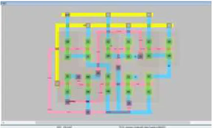
P a g e | 377 Figure9: SISO implementation by using four D flipflops layout diagram
IV SIMULATION RESULTS
Figure.10.existed gdi based D flip flop Simulation waveform.
Figure11: gdi based D flip flop using pmos as delay element Simulation waveform.
Figure12: proposed gdi based D flip flop using nmos as delay element Simulation waveform.
Extension circuit waveforms: SISO:
Figure.13.wavefo rms of
siso
with basic D flip flops multiplexer Simulation.Figure.14.Waveforms of
siso
with proposed nmos as a delay element D flip fops multiplexer Simulation.Table-I
Po wer comparisions Between Existed and Proposed GDI Bas ed D Flip Flop.
Parameters
Existed GDI based D- flip flop
PMOS used as Delay Element
NMOS used as Delay Element POW ER 2.0085µW 1.4827µW 909.17nW Table-II
Co mp arison of Transistor Count With Existed and Pro posed D flip flop.
Parameter Existing circuit
Pmos used as delay element
Nmos used as delay element Area
(transistor co unt)
12 11 11
Tab le-III
Co mp arison of Simulation siso with existed and Pro posed D flip flop
Parameter Existed gdi based D- flip flops
Proposed gdi based D- flip flops
Available online:
http://edupediapublications.org/journals/index.php/IJR/
P a g e | 378V CONCLUSION
Digital logic sub threshold operation is introduced briefly as a means to achieve very h igh energy savings, and ultra low power for systems which do not have high performance requirements. However, due to the high sensitivity of the sub threshold circu its to process variations, it is imperative to use innovative design techniques to improve circu it robustness. Further, in order to achieve optimal performance, device, and circuit architecture level optimizations, specific to the sub threshold circuits need to be applied. Sub threshold operation is suited for circuits which have low frequency requirements. Sub threshold region compared to the super threshold region such as exponential dependence of current on gate voltage, lower intrinsic gate capacitance, Because of these differences, conventional design techniques may yield suboptimal results. Comparisons show that proposed circuit is the best. The experimental results verify that GDI is superior to other styles.
REFERENCES
[1]Su meet Ku mar Gupta, A rijitRaychowdhury, and Kaushik Roy, Fellow IEEE , Dig ital Co mputation in Subthreshold Region for Ultralo w-Po wer Operation: A Device– Circuit–Architecture Codesign Perspective‖, Vo l. 98, No.2,February 2010 |Proceedings of the IEEE.
[2] Sagi Fisher, Adam Teman, Dmitry Vaysman, Alexander Gertsman,Orlyadid-Pecht, ―Ultra-Low Power Subthreshold Flip-Flop Design‖,ISCAS 2009,IEEE international symposium on Circuits and systems, pp. 1573-1576.
[3] Arkadiy Morgenshteid, Alexander Fish2 and Israel A. Wagner3 Gate- diffusion input (GDI) –a novel power efficient method for digital circu its: A design methodology 0-7803-6741-3~901/$10.000 2001 IEEE.
[4] J. Kwong, Y. Ramadass, N. Verma, M . Koesler, K. Huber, H. Moormann, and A. Chandrakasan, BA 65 n m Sub-Vt microcontroller with integrated SRAM and switched-capacitor DC-DC converter, in Proc. IEEE ISSCC, Feb. 2008, pp. 318–319.
[5] K. Roy, S. Mukhopadhyay, H. Mahmoodi - Meimand, ―Leakage Current Mechanisms and
Leakage Reduction Techniques in Deep-Submicro meter CMOS Circu its‖.Proceedings of the IEEE, vol. 91, no.2, Feb. 2003.
[6] S. Kang, "Elements of Low Po wer Design for Integrated System “ISLPED”03, August,2003.
[7] A. Morgenstein, A. Fish, I. Wagner, ―An Efficient Imp lementation of D-Flip-Flop Using the GDI Technique,‖ ISCAS ’04, pp. 673-676, May 2004.
[8 ]A. Morgenshtein, A. Fish, I.A. Wagner, ―Gate-Diffusion Input (GDI) – Power Efficient Method for Dig ital Co mbinatorial Circuits,‖ IEEE Trans. VLSI, vol. 10, no. 5, pp. 566-581, October 2002.
[9] Wang, B. H. Calhoun and A. Chandrakasan, ―Sub-threshold design forultra low-power systems‖.Springer publishers, 2005.
A UTHOR’S BIOGRAPHY
Author1:D.Anil Ku mar Persued B.Tech with stream electronics and communication engineering from Pace Institute of technology and sciences,ongole JNTUKuniversity.Persuing M.Tech with stream VLSI&ES from Pace Institute of technology and sciences,ongole JNTUKuniversity.
.
Author2:M r.K.Sundeep working as assosiate professor in Pace Institute of technology and sciences,Ongole. He is having eight years of experience in teaching.