Design and Implementation of Terahertz Near-Field Imaging Of
Dielectric Resonators
1.SAPAVAT DEEPA
ABSTRACT:
As an alternative to metallic resonators, dielectric resonators can increase radiation efficiencies of metasurfaces at terahertz frequencies. Such subwavelength resonators made from low-loss dielectric materials operate on the basis of oscillating displacement currents. For full control of electromagnetic waves, it is essential that dielectric resonators operate around their resonant modes. Thus, understanding the nature of these resonances is crucial towards design implementation. To this end, an array of silicon resonators on a quartz substrate is designed to operate in transmission at terahertz frequencies. The resonator dimensions are tailored to observe their low-order modes of resonance at 0.58 THz and 0.61 THz respectively. We employ a terahertz near-field imaging technique to measure the complex near-fields of this dielectric resonator array. This unique method allows direct experimental observation of the first two fundamental resonances.
1. INTRODUCTION
Metasurfaces or two-dimensional
metamaterials [1] consist of miniaturized
resonators with subwavelength periodicity,
and are capable of manipulating the
wavefront of incident waves. The principle
of metasurfaces to control the wavefront
reconciles with that of reflectarrays [2] and
transmitarrays [3], well established at
microwave frequencies. Conventionally,
metallic resonators are employed for
shaping wavefronts either through reflection
[2, 4] or transmission by using multilayer
configurations [5,6]. Typically, metallic
resonators exhibit decreasing radiation
efficiencies with increasing frequencies.
This is due to increasing Ohmic loss at
frequencies beyond the microwave regime
[7]. In contrast, metasurfaces made of
dielectric resonators have been shown to
intrinsically maintain high efficiencies from
the microwave to the visible frequency
range [8, 9]. As dielectric resonators operate
based on the oscillation of displacement
current at specific resonance frequencies,
Ohmic loss is alleviated, and dielectric
losses can be minimized through the use of
low-loss dielectric materials [10]. Apart
from the superior efficiency as discussed
above, dielectric resonators can support
dielectric layer, as opposed to two layers
required by their metal counterparts. With
proper magnetic and electric resonances,
dielectric resonator metasurfaces can exhibit
extraordinary phase, amplitude and
polarization control of output waves. As for
the phase control, individual resonators can
induce a phase discontinuity within the 2π
range for shaping the outgoing wavefront in
transmission [11–13] and reflection [8, 9,
14]. A number of components have
exploited electric and magnetic resonances
in dielectric resonators for different
functions, which include generation of
holograms [15] and optical vortices [16].
Other research works have demonstrated
ways to mechanically tune dielectric
resonator arrays as crucial steps towards
implementing high performance
reconfigurability [17, 18]. In the terahertz
frequency regime, high-efficiency
components are particularly important as
power is generally limited and there is
degradation in the signal-to-noise ratio due
to free-space path loss and atmospheric
absorption. Practical applications for
terahertz metasurfaces of subwavelength
metallic resonators have been proposed in
sensing [19–22], filtering [23] and
wavefront manipulation [24–28]. Dielectric
resonators have the potential to become
crucial building blocks in the terahertz
frequency region by increasing the
efficiency of basic components. Magnetic
mirrors and reflectarrays based on dielectric
resonators that exploit the properties of
magnetic resonances have been realized
with high performance [29, 30]. Terahertz
dielectric resonators that utilize overlapping
magnetic and electric resonances have been
designed and experimentally validated.
Some applications include extraordinary
wavefront manipulation in reflection [31]
and a highly efficient absorber [32].
Currently, most metasurfaces are
characterized by far-field measurements
using terahertz time-domain spectroscopy
systems (THz-TDS). However, terahertz
far-field measurements are lacking the
microscopic resolution needed to investigate
the properties of samples in the near- field.
Importantly, reactive near-fields cannot be
observed through far-field measurement. In
contrast, terahertz near-field microscopy has
been useful in mapping the two-dimensional
electromagnetic responses of various
samples with spatial resolutions below the
diffraction limit [33–35]. Some components
characterized by terahertz near-field
microscopy include metallic resonators [36–
38], metallic subwavelength holes [39] and
No. 4 | 20 Feb 2017 | OPTICS EXPRESS
3758 high-permittivity TiO2 (εr ≈ 100) [40].
Here, we conduct a near-field measurement
to examine the properties of the fundamental
electric and magnetic dipole resonances of a
dielectric resonator array, fabricated via a
top-down approach. Understanding these
fundamental resonances is essential towards
designing highly efficient metasurfaces.
2. DESIGN OF TERAHERTZ
DIELECTRIC RESONATORS A
terahertz dielectric resonator array is
constructed from periodically arranged
silicon cylinders on a quartz substrate. The
cylindrical shape of the resonator is chosen
mainly because of its isotropy. Furthermore,
periodically arranged cylindrically shaped
resonators are worth investigating due to
their practicality for planar integration and
robustness in design implementation,
particularly for wave manipulation with
metasurfaces. In addition, inter-resonator
coupling that exists within arrays cannot be
observed in an individual resonator. The
operation of dielectric resonators can be
described by their quality factors: This
includes Qrad, which is inversely
proportional to radiation loss, and Qd iss
which is inversely proportional to energy
loss to dissipation in the materials. It is not
advisable to have high Qrad as a sharp
resonance only allows for narrowband
operation of metasurfaces. For potential
applications in wave manipulation over a
relatively large bandwidth, it is ideal that the
dielectric resonator exhibits a high Qd iss
and moderate Qrad. Thus, high-resistivity
float-zone silicon is chosen as the dielectric
material as it has moderate relative
permittivity εr = 11.68 and negligible loss
[41]. The substrate is quartz with thickness
of 500 µm and relative permittivity εr = 3.8
with loss tangent tan δ = 0.01 [42]. The
structure has high Qd iss as low-loss
dielectrics have been utilized in the design
and moderate Qrad as the resonator has a
moderate effective permittivity. As our
quartz substrate is more than one
wavelength thick, it contributes to the
resonance properties of our dielectric
resonator array. The resonator height of 82
µm and the radius of 105 µm are selected to
exhibit electric and magnetic dipole
resonances centered around 0.60 THz. The
unit cell of the dielectric resonator array is
245 µm which is explicitly chosen to be less
than half the operating wavelength (λ = 500
µm) to avoid diffraction. Numerical
computations are performed by using the
frequencydomain solver in CST Microwave
Studio. The periodic boundary conditions
infinite uniform array of the resonators. The
fundamental modes of resonance excited in
this dielectric resonator array are the TM01δ
for the electric dipole resonance and the
HEM11δ for the magnetic dipole resonance
[10]. We can classify the electric and
magnetic dipole resonance modes by
examining their electric and magnetic fields,
as revealed by cross-sectional views in Fig.
1. The electric dipole resonance (Fig. 1a)
shows an electric field that is oscillating in
the direction of the incident wave’s
polarization (Ey ). Magnetic dipole
resonances (Fig. 1b) can be identified with a
circulating electric field around the center of
the resonator. The symmetry of the periodic
array in the xy-plane induces symmetric
mutual coupling, and thus the field
distribution shows the corresponding
symmetry, in the y-direction. Due to the
presence of a substrate in the dielectric
resonator array, free-space illumination from
the +z direction causes asymmetry of the
field distribution in the z-direction.
3. FABRICATION For this structure,
micro-fabrication approach involves a
combination of SU-8 assisted bonding,
photolithography, and deep reactive ion
etching (DRIE). To begin with, a thin
adhesion layer of SU-8 is spin-coated on a
3-inch quartz wafer. A 125 µm thick,
high-resistivity silicon wafer is then bonded to the
substrate by passing it through a laminator at
100 ◦C at slow speed. The bonded silicon is
thinned down as per the design requirements
by plasma-enhanced DRIE (Oxford
PlasmaPro 100 Estrelas). Finally, the silicon
layer is patterned with thick photoresist
(AZ4562) and subsequently etched down
with the Bosch silicon etching process to
realize an
Fig. 1. Cross-sectional view of a single
dielectric resonator. The instantaneous
electric fields are represented by blue
arrows. (a) Electric dipole resonance and (b)
incident from the substrate side, and it is
polarized in the y-direction.
array of cylinders. It should be noted that,
considering the low thermal conductivity of
quartz, the aforementioned etching steps are
performed at -5 ◦C. Fabricated structures are
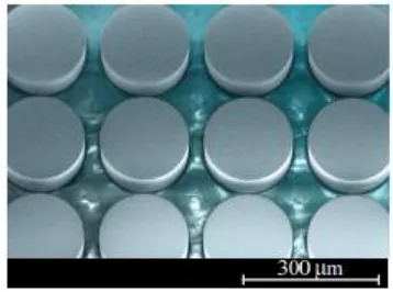
imaged using scanning electron microscopy
(FEI Verios SEM). False-color and optical
profiler images of the fabricated dielectric
resonator array are shown in Fig. 2 and in
Fig. 3 respectively. These images are
representative of the impeccable quality and
high detail accuracy of the fabricated
samples.
Fig. 2. Scanning electron micrograph of the fabricated silicon resonators.
Fig. 3. Optical profiler image of the
fabricated silicon resonators. The
dimensions are as follows: the unit cell size
a = 245 µm, the resonator height h = 82 µm,
and the resonator radius r = 105 µm.
4. MEASUREMENTS AND RESULTS
4.1. FAR-FIELD ANALYSIS AND
RESULTS A standard THz-TDS system is
used for far-field measurements. A focused
beam with a spot size of 5 mm illuminates
the sample from the substrate side to excite
approximately 300 dielectric resonators. A
measurements are conducted in a
nitrogen-purged atmosphere to mitigate the water
vapour absorption. Fourier transform is
applied to the time-resolved data to obtain
the complex frequency response of the
sample with a spectral resolution of 5 GHz.
The transmission amplitude is shown in Fig.
4. From the normalized spectrum, we can
observe the dips at 0.58 THz and 0.61 THz
which correspond to the electric dipole
resonance and magnetic dipole resonance
respectively. The strength and position of
these resonances differ slightly from the
results obtained from numerical simulation
with CST Microwave Studio. This could be
due to the realized focused beam as opposed
to numerical plane-wave approximation
[43]. A relatively large resonance width can
be observed in Fig. 4 which corresponds to a
moderate Qrad factor, as designed. Based on
theoretical calculations in [10], we would
expect a lower Qrad factor for a magnetic
dipole resonance (Qrad = 9.15) as compared
to an electric dipole resonance (Qrad =
9.43). This is because the field distribution
of the magnetic dipole resonance is less
confined within the dielectric resonator
resulting in a slightly lower radiative Q
factor as compared to the electric dipole
resonance. Apart from that, higher-order
modes can also be observed at higher
frequencies in both the simulation and
measurement.
4.2. NEAR-FIELD SETUP AND
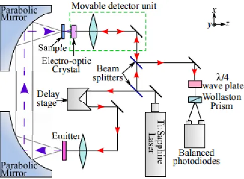
ANALYSIS As shown in Fig. 5, the
near-field experiment setup is based on a typical
THz-TDS system, with the major difference
being that the electro-optic crystal is placed
very close to the sample to collect reactive
fields emerging from the sample. In order to
measure the longitudinal electric fields, Ez ,
we used an electro-optic crystal in the (100)
orientation. The dielectric resonator array is
illuminated from the back of the substrate
with a y-polarized focused Gaussian beam
with a spot diameter of 500 µm. The Ez
field measurement is taken at approximately
100 µm (λ0/5) above the dielectric resonator
array to minimize electric field disturbance.
It is also possible to measure the transverse
components, Ex and Ey using electro-optic
crystals of the (110) orientation [44].
However, measurements of the transverse
components (Ex and Ey ) are not utilized in
this work, since local evanescent transverse
components outside the dielectric resonators
are relatively weak. This weak field is
obscured by the propagating terahertz waves
that co-propagate with the probe beam
throughout the crystal length. It is
apertures [45] and planar metamaterials [37], it is possible to
Fig. 4. Normalized transmission spectra of the dielectric resonator array
Fig. 5. Near-field THz-TDS experimental set up. The purple arrows represent the THz pulses and the red arrows indicate the infrared laser beam paths.
measure all three components of the electric
field, owing to their exposed strong
localized field. The employed near-field
system can measure the electric field in one
spot at a time with a spot diameter of 10 µm
which is defined by the probe laser. A 2D
raster scan is performed by moving the
electro-optic crystal together with the laser
beam with translation stages. The
longitudinal (z-directed) electric fields hence
is mapped over the xy plane with a spatial
resolution of 20 µm. A complete set of
measurements for each near-field spot
consists of a total electric field measurement
of the Ez component, Ez,t(t), in the presence
of the sample, and a reference or incident
electric field measurement Ez,r (t),
measured with a bare quartz substrate
replacing the sample. To obtain the scattered
field due to interaction with the resonator
solely, we subtract the reference electric
field from the total electric field in the
frequency domain. From data analysis a
slight temporal shift is observed between the
reference and sample measurements. To
mitigate the effect of this shift, a phase
offset (∆φ) can be added to the reference
measurement: A slight spatial misalignment
of the measured results is also observed in
the xy dimensions. This can be
straightforwardly compensated by shifting
the alignment between the sample and
reference data.
4.3. NEAR-FIELD RESULTS As a
comparison, we simulate the dielectric
resonator array with CST Microwave
Studio, with a 100 µm air gap space between
electro-optic crystal (εr = 2.25) and sample
to match experimental conditions. The
measured and simulated instantaneous
electric fields for both electric and magnetic
dipole resonances are shown in Fig. 6. The
fields are at the moment when the oscillation
reaches their maximum amplitude and are
also normalized to the maximum amplitude
of the electric fields for the simulated
magnetic dipole resonance. The measured
near-field images show horizontal variations
in amplitude which are due to the focused
beam used during measurement. From the
simulations, we can observe that the Ez field
for the magnetic resonance is stronger than
the electric resonance. As both simulated
and measured plots are normalized to the
same scale, the same observation is
confirmed in the measured results. This
relatively strong Ez field is due to the
out-of-the-plane circulation of the electric field
for the magnetic resonance.
CONCLUSION In conclusion, we have
designed and experimentally validated an
array of terahertz dielectric resonators
operating in transmission at terahertz
frequencies. As the resonant electric fields
are mostly confined within the dielectric
resonators themselves, these fields are not
readily accessible via near-field probe. This
is in contrast to metallic resonators where
resonant electric fields are not confined
within the structure facilitating access to
near-field transverse electric field
components. Nevertheless, we have
investigated dielectric resonator structures
with both far- field spectroscopy and
near-field spectroscopy. We achieved good
agreement between our measured and
simulated results for both the far-field and
near-field measurements. With near-field
THz-TDS techniques, we confirm the
presence of the predicted fundamental
magnetic resonance mode at 0.61 THz.
Electromagnetic interactions between the
resonators observed in the near-field
provides information that cannot be obtained
in the far-field which is useful for potential
future applications of metasurfaces.
REFERENCES AND LINKS
1. N. I. Zheludev and Y. S. Kivshar,
“From metamaterials to metadevices,”
Nat. Mater. 11, 917–924 (2012).
2. J. Huang and J. A. Encinar,
Reflectarray Antennas, vol. 30 (John
Wiley & Sons, 2007).
3. C. G. Ryan, M. R. Chaharmir, J.
Shaker, J. R. Bray, Y. M. Antar, and
A.
Ittipiboon,
“A
wideband
transmitarray
using
dual-resonant
double square rings,” IEEE Trans.
Antennas Propag. 58, 1486–1493
(2010).
4. N. Yu, P. Genevet, M. A. Kats, F.
Aieta, J.-P. Tetienne, F. Capasso, and
Z. Gaburro, “Light propagation with
phase
discontinuities:
generalized
laws of reflection and refraction,”
Science 334, 333–337 (2011).
5. C. Pfeiffer, N. K. Emani, A. M.
Shaltout, A. Boltasseva, V. M.
Shalaev, and A. Grbic, “Efficient light
bending with isotropic metamaterial
Huygens’ surfaces,” Nano Lett. 14,
2491–2497 (2014).
6.
C. Pfeiffer
and
A.
Grbic,
“Cascaded metasurfaces for complete
phase and polarization control,” Appl.
Phys. Lett. 102, 231116 (2013).
7. J. B. Khurgin, “How to deal with
the
loss
in
plasmonics
and
metamaterials,” Nature 10, 2–6
(2015).
8. L. Zou, W. Withayachumnankul, C.
M. Shah, A. Mitchell, M. Klemm, M.
Bhaskaran,
S.
Sriram,
and
C.
Fumeaux, “Efficiency and scalability
of dielectric resonator antennas at
optical frequencies,” IEEE Photon. J
6, 1–10 (2014).
9. L. Zou, W. Withayachumnankul,
Bhaskaran,
S.
Sriram,
and
C.
Fumeaux,
“Dielectric
resonator
nanoantennas at visible frequencies,”
Opt. Express 21, 1344–1352 (2013).
10. A. Petosa, Dielectric Resonator
Antenna Handbook (Artech House
Publishers, 2007).
11. I. Staude, A. E. Miroshnichenko,
M. Decker, N. T. Fofang, S. Liu, E.
Gonzales, J. Dominguez, T. S. Luk,
D. N. Neshev, I. Brener, and Y.
Kivshar,
“Tailoring
directional
scattering through magnetic and
electric resonances in subwavelength
silicon nanodisks,” ACS Nano 7,
7824–7832 (2013).
12. F. Wang, Q.-H. Wei, and H.
Htoon, “Generation of steep phase
anisotropy with zero-backscattering
by arrays of coupled dielectric
nano-resonators,” Appl. Phys. Lett. 105,
121112 (2014).
13. Q.-T. Li, F. Dong, B. Wang, F.
Gan, J. Chen, Z. Song, L. Xu, W.
Chu, Y.-F. Xiao, Q. Gong, and Y. Li,
“Polarizationindependent and
high-efficiency dielectric metasurfaces for
visible light,” Opt. Express 24,
16309–16319 (2016)
AUTHOR’SPROFILE:
SAPAVAT DEEPA
Received the B.Tech degree in Electronics & Communication Engineering from Sree Dattha Institute of Engineering & Science 2013 from JNTU, Hyderabad, Telangana, India and She completed M.Tech in
Electronics & Communication Engineering as specialization in the Department of Electronics & Communication Engineering in 2017 from JNTU Hyderabad Teangana India. She is currently an Assistant Professor with the Department Electronics &
Communication Engineering. at SLC College Jntu University, Hyderabad, Telangana India. Her research interests include in the area of RF and Microwave
Engineering andOptical networks.