ISSN (Print) : 2320 – 3765 ISSN (Online): 2278 – 8875
I
nternational
J
ournal of
A
dvanced
R
esearch in
E
lectrical,
E
lectronics and
I
nstrumentation
E
ngineering
(An ISO 3297: 2007 Certified Organization)
Vol. 5, Issue 2, February 2016
Efficient Vedic Multiplication Oriented
Pipeline Architecture with Booth/Baugh
Wooley Comparisons
R.Dhivya, S. Maheshwari
PG Scholar, Department of Electronics and Communication, Mookambigai College of Engineering, Pudukottai, India
Assistant Professor, Department of Electronics and Communication, Mookambigai College of Engineering, Pudukottai,
India
ABSTRACT: The system contain a high speed low power digital multiplier by using advantage of Vedic multiplication algorithms with a very efficient leakage control technique called multiple channel CMOS (Mc CMOS) technology. We have designed 16 bit Vedic multiplier using McCMOS technology and used 65nm and 45nm node technology and comparative simulation results that indicates the performance of the circuit. Vedic mathematics is an ancient Indian mathematics is very useful for doing tedious and cumbersome mathematical calculation at a very fast rate. The Vedic Urdhva-Tiryakbhyam multiplier is approximately 10 times faster performance than the conventional multiplier architecture. Thorough simulations of 32 x 32 digital Vedic multiplier we are using McCMOS Technology which show the Power Delay Product (PDP) is reduced by approximately 75 % compared to the conventional multiplier design. The simulations have been carried out in cadence-spice simulator with 1V power supply. This technique will be very useful for designing low leakage high speed ALU unit. In the first phase of work we implemented the 32 bit Vedic multiplication operation and in the second phase we further extend our work into the comparisons of Booth and Baugh Wooley with Pipelined Architecture.
KEYWORDS: Vedic Multiplication Algorithm, Multi Channel CMOS Technology, Vedic Urdhva-Tiryakbhyam multiplier, Power Delay Product PDP).
I.INTRODUCTION
Reduction of area power dissipation and propagation delay is one of major area concern in modern VLSI Design. This system presents an efficient technique is used for multiplication of two binary numbers which reduce the average power, leakage power and delay. The proposed architecture is based on Urdhva-Tiryakbhyam Sutra of Vedic mathematics to increase the speed performance of binary multiplication which is based on 16 sutra (formula). This idea of designing the multiplier from Vedic mathematics is come because partial product and sum are generated in single step. An efficient Design technology for leakage control and McCMOS (Multiple- Channel CMOS) has been used for power and performance optimization of the Vedic Multiplier. The organization of this system is as follow: it contains MOSFET scaling and McCMOS technique, section 3 contains conventional binary multiplication algorithm and proposed algorithm of multiplication based on the Urdhva-Tiryakbhyam Sutra of Vedic mathematics has been described. Reduction of power dissipation and propagation delay is one of the main areas of concerns in modern VLSI designs. Keeping that in mind, an efficient technique for multiplication of two binary numbers with reduced average and leakage power and delay is presented in this system. The proposed architecture is based on the Urdhva-Tiryakbhyam Sutra of Vedic mathematics in order to enhance the speed of the binary multiplication [3, 8]. In the algorithmic and structural level a lot of other multiplication techniques have been developed for enhancing the efficiency of multiplier. But the idea of designing the multiplier from Vedic mathematics has emerged as in this technique the partial products and the sums are generated in only a single step. The use of Vedic Urdhva-Tiryakbhyam multiplier achieves approximately 10 times faster performance than the conventional multiplier architecture.
ISSN (Print) : 2320 – 3765 ISSN (Online): 2278 – 8875
I
nternational
J
ournal of
A
dvanced
R
esearch in
E
lectrical,
E
lectronics and
I
nstrumentation
E
ngineering
(An ISO 3297: 2007 Certified Organization)
Vol. 5, Issue 2, February 2016
MOSFET Scaling McCMOS Technique
In the MOS technology, the scaling parameters of the MOSFET’s are critical. Such as channel length (Lc), Junction depth (Xj), channel doping (N), gate oxide thickness (Tox).The generalized equation for channel length
Where Lmin is the minimum channel length for which long channel sub-threshold behaviour will be observed, A is proportionality constant, Xj is junction depth, Tox is oxide thickness, Ws is the source depletion depth Wd is the drain depletion depth in a one dimensional abrupt junction formulation. Vds is the drain to source voltage, Vbi built in voltage of the junctions and VBS body to source reverse bias. The key parameter of the MOSFET scaling is described by Taur, Buchanan.
Fig.1 Inverter Using the 45nm McCMOS Technique
ISSN (Print) : 2320 – 3765 ISSN (Online): 2278 – 8875
I
nternational
J
ournal of
A
dvanced
R
esearch in
E
lectrical,
E
lectronics and
I
nstrumentation
E
ngineering
(An ISO 3297: 2007 Certified Organization)
Vol. 5, Issue 2, February 2016
indicates that the leakage reduction by a factor of at least 150 with only small increase in circuit area and switched capacitance. Leakage current can be controlled by increasing the channel length. Reducing the channel length would decrease the threshold voltage which seems to be a great challenge in designing small devices. In non- critical path we will increase the channel length of at least one transistor (prefer one which have high probability of turn off) in each possible current path between Vdd and ground. In critical path apply the same technique but increase transistor width as necessary to maintain performance. The main advantage of McCMOS technique is its simplicity. One has to just increase the channel length very merely of the selected transistors which can be easily accomplished by existing CAD tools and single Vth Processor, another advantage of McCMOS technique is leakage control can be possible for both active and idle mode of circuit operation. A simple example of an inverter is shown in Fig. 1. Where 45 nm McCMOS technique has been used for the power optimization of the circuit.
The key parameters are power supply and threshold voltage, short-channel effect, gate oxide, current carrying capability and leakage current limit. In deep submicron CMOS design, non-minimum length transistors offer the possibility of achieving excellent leakage control without the disadvantages of other known leakage control techniques. Initial analysis of the circuits using McCMOS technique indicates that one can expect leakage reduction by a factor of at least 150 with only modest increase in circuit area and switched capacitance. Controlling the leakage current can be done by increasing the channel length that has been proposed in this paper. Doubling the channel length would give us a leakage saving ratio in the order of 250.Now reducing the effective channel length would decrease the threshold voltage which seems to be a great challenge in designing small devices.
In the noncritical path of a circuit we should increase the channel length of at least one transistor (preferably one with a high probability of being turned off) in each possible current path between Vdd and ground. In critical paths, apply the same technique but increase transistor width as necessary to maintain performance.
The main advantage of McCMOS technique than other leakage control circuits is its simplicity. One has to just increase the channel length very merely of the selected transistors which can be easily accomplished by existing CAD tools and single VTH processes. In other techniques other processing steps may be required. Another very significant advantage of McCMOS technique is that leakage control can be possible for both active and idle mode of circuit operation. A simple example of an inverter is shown in Fig. 1. Where 45 nm McCMOS technique has been used for the power optimization of the circuit. As seen from the circuit we have used non minimum length of selected transistor for controlling the leakage power.
Conventional Multiplier Algorithm
The multiplication algorithm for an 8×8 multiplication process is shown in Fig. 2. Multiplicands are denoted by ai and multipliers are denoted by bi, where i=0 to 7 for an eight bit multiplier. Pi are the partial products, where i=0, 1, . . .63. These partial products are added by using half adders and full adders. The ovals containing three bits are the full adders and those containing two bits are the half adders. After the addition, the sums are denoted by Si and carries are denoted by Ci, where ‘i’ denotes the column number of the added bits. There are sixteen columns that started with 0 from the right side. The bits that are not in the oval are forwarded to the next stage without any Boolean operation; these bits are shown in bold letters.
ISSN (Print) : 2320 – 3765 ISSN (Online): 2278 – 8875
I
nternational
J
ournal of
A
dvanced
R
esearch in
E
lectrical,
E
lectronics and
I
nstrumentation
E
ngineering
(An ISO 3297: 2007 Certified Organization)
Vol. 5, Issue 2, February 2016
Fig.2 Conventional Multiplier Algorithm
ISSN (Print) : 2320 – 3765 ISSN (Online): 2278 – 8875
I
nternational
J
ournal of
A
dvanced
R
esearch in
E
lectrical,
E
lectronics and
I
nstrumentation
E
ngineering
(An ISO 3297: 2007 Certified Organization)
Vol. 5, Issue 2, February 2016
Figure 3 Urdhva-Tiryakbhyam 4×4 multiplication procedures.
II.PROBLEM STATEMENT
In sub-micron CMOS design, non-minimum length transistors offer the possibility of achieving excellent leakage control without the disadvantages of other known leakage control techniques. Preliminary analyses indicate that one can expect leakage reduction by a factor of at least 100 (and possibly orders of magnitude higher) with only modest increases in circuit area and switched capacitance. This paper briefly reviews related leakage control techniques, describes the McCMOS technique, and presents: simulation results that are indicative of the performance of the technique.
A scalable architecture for pipelined and iterative Wallace tree multipliers is presented. For netlist-only multipliers, minimal latency and number of pipeline stages are achieved through a decay-driven design scheme. The architecture can be modified to a tree-of-Wallace-trees structure for regular layout, at the expense of latency. The achievable minimal cycle time equals the delay through two full adder cells, plus the setup time and delay through a register. The elemental Wallace trees in this architecture can also be used in iterative structures that provide a variety of delay/gate-count tradeoffs.
ISSN (Print) : 2320 – 3765 ISSN (Online): 2278 – 8875
I
nternational
J
ournal of
A
dvanced
R
esearch in
E
lectrical,
E
lectronics and
I
nstrumentation
E
ngineering
(An ISO 3297: 2007 Certified Organization)
Vol. 5, Issue 2, February 2016
A complementary all-N-transistor (CANT) comprising the ANT logic and a novel inverted ANT logic are proposed in this paper. The threshold voltage of the transistors in the ANT logicpsilas N-block is variable depending upon the operation of the entire logic block. In the evaluation phase, the bulk voltage of the transistors in the N-block is raised to VDD - Vthn such that the drain current therein is increased to enhance operation speed. In the pre-charge phase, the bulk voltage of those transistors in the N-block is reduced to its normal voltage level such that the sub threshold leakage current is dropped to reduce power consumption. By utilizing such a variable bulk voltage scheme in the CANT, a 32-bit CLA is designed to justify the low power and high speed performance. The power dissipation is 143 mW at 5.4 GHz clock rate given the worst PVT (SS, 1.08 V, 75degC) condition.
Starting with a brief review on 0.1-μm (100 nm) CMOS status, this paper addresses the key challenges in further
scaling of CMOS technology into the nanometer (sub-100 nm) regime in light of fundamental physical effects and practical considerations. Among the issues discussed are: lithography, power supply and threshold voltage, short-channel effect, gate oxide, high-field effects, dopant number fluctuations and interconnect delays. The last part of the paper discusses several alternative or unconventional device structures, including silicon-on-insulator (SOI), SiGe MOSFET's, low-temperature CMOS, and double-gate MOSFET's, which may lead to the outermost limits of silicon scaling.
III.APPROACH
Proposed Algorithm using Ancient Mathematical Approaches Urdhva-Tiryakbhyam
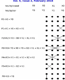
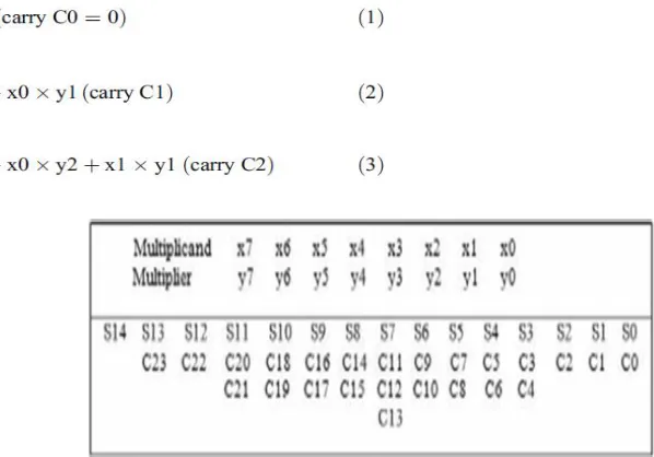
The contribution of ancient Indian mathematics in the world history of mathematics has been immense. Vedic mathematics is one such a system of ancient Indian mathematics, which enables different mathematical operations to be carried out at a very brisk rate. It uses various formulas used for fast calculations. “Urdhva-Tiryakbhyam” Sutra is such a general formula applicable to all cases of multiplication. The meaning of this sutra is “vertically and crosswise”. Figure 4 represents the general multiplication procedure of 4×4 multiplier using the above sutra. This figure depicts the generation of different partial products and addition of them to get the final multiplier output.X0*Y0 is a partial product which is the 1st bit of the multiplier output, P0. In the next step X1*Y0 & X0*Y1 are two partial products and by adding them we get P1. In this way we get P2, P3... P6 and consequently the final 7bit output of the 4×4 multiplier. The multiplication algorithm for an 8×8 multiplier is shown below. Multiplicands are denoted by xi and multipliers are denoted by yi where i=0,1,…7 for a 8 bit multiplier. The bits of multiplicand and multiplier are multiplied vertically and crosswise stated in the Urdhva-Tiryakbhyam sutra to generate the partial products. These partial products are added using half and full adders. Thus the partial products and sums are generated in only a single step. The output of the adders are Sm where m=0, 1,……14 & Cn n=0, 1,….23. Generation of sums of partial products and carrys has been shown in the above Fig. 5. and subsequent equations below.
ISSN (Print) : 2320 – 3765 ISSN (Online): 2278 – 8875
I
nternational
J
ournal of
A
dvanced
R
esearch in
E
lectrical,
E
lectronics and
I
nstrumentation
E
ngineering
(An ISO 3297: 2007 Certified Organization)
Vol. 5, Issue 2, February 2016
Fig.5 Generation of final multiplier output.
Fig.6 Comparative Study of Average Power
IV.BLOCK DIAGRAM
ISSN (Print) : 2320 – 3765 ISSN (Online): 2278 – 8875
I
nternational
J
ournal of
A
dvanced
R
esearch in
E
lectrical,
E
lectronics and
I
nstrumentation
E
ngineering
(An ISO 3297: 2007 Certified Organization)
Vol. 5, Issue 2, February 2016
In the first phase of work we implemented the 32 bit Vedic multiplication operation and in the second phase we further extend our work into the comparisons of Booth and Baugh Wooley with Pipelined Architecture.
There are a wide range of multiplication techniques; the one perhaps most familiar to the majority of people is the classic long multiplication algorithm, e.g.
23958233 5830 × ---
00000000 (= 23,958,233 × 0) 71874699 (= 23,958,233 × 30) 191665864 (= 23,958,233 × 800) 119791165 (= 23,958,233 × 5,000) ---
139676498390 (= 139,676,498,390)
While this algorithm works for any pair of numbers, it is long winded, requires many intermediate stages, and requires you to record the results of each of the intermediate stages so you can sum them at the end to produce the final answer. However, when the numbers to be multiplied fall into certain categories, short-cuts can be used to avoid much of the work involved in long multiplication. There are many of these 'special cases' some of them allow seemingly difficult multiplications to be completed mentally, literally allowing you to just write down the answer. To multiply two-digit numbers the normal way, you would have to multiply the ones place by the other number then multiply again by the tens place, but there is another way. Vedic math can help you solve what would be a hard problem, easily. There are sixteen different "sayings" in Vedic math, but here is just one: "Vertically and horizontally."
The proposed architecture is based on Urdhva-Tiryakbhyam Sutra of Vedic mathematics to increase the speed performance of binary multiplication which is based on 16 sutra (formula). This idea of designing the multiplier from Vedic mathematics is come because partial product and sum are generated in single step. An efficient Design technology for leakage control and McCMOS (Multiple- Channel CMOS) has been used for power and performance optimization of the Vedic Multiplier. The organization of this system is as follow: it contains MOSFET scaling and McCMOS technique, section 3 contains conventional binary multiplication algorithm and proposed algorithm of multiplication based on the Urdhva-Tiryakbhyam Sutra of Vedic mathematics has been described.
Reduction of power dissipation and propagation delay is one of the main area of concerns in modern VLSI designs. Keeping that in mind, an efficient technique for multiplication of two binary numbers with reduced average and leakage power and delay is presented in this paper. The proposed architecture is based on the Urdhva-Tiryakbhyam Sutra of Vedic mathematics in order to enhance the speed of the binary multiplication [3, 8]. In the algorithmic and structural level a lot of other multiplication techniques have been developed for enhancing the efficiency of multiplier. But the idea of designing the multiplier from Vedic mathematics has emerged as in this technique the partial products and the sums are generated in only a single step. The use of Vedic Urdhva-Tiryakbhyam multiplier achieves approximately 10 times faster performance than the conventional multiplier architecture.
Furthermore, an efficient design technology for leakage control, McCMOS (multiple channel CMOS), has been used for the power and performance optimization of the Vedic multiplier. It is shown that by using this technique a much better performance is achieved than the conventional multiplier using CMOS architecture which will be quite helpful for high performance computing.
V.SIMULATION RESULTS
ISSN (Print) : 2320 – 3765 ISSN (Online): 2278 – 8875
I
nternational
J
ournal of
A
dvanced
R
esearch in
E
lectrical,
E
lectronics and
I
nstrumentation
E
ngineering
(An ISO 3297: 2007 Certified Organization)
Vol. 5, Issue 2, February 2016
multiplier. Table 2 encompasses the experimental results of McCMOS conventional and McCMOS Urdhva-Tiryakbhyam multiplier. It can be clearly seen from the tables that with the use of Urdhva-Urdhva-Tiryakbhyam rule and McCMOS technique the performance of the multiplier can be considerably improved.
Urdhva-Tiryambakam
Multiplication has some limits and to overcome these limitations a new approach has been describe and designed a Vedic multiplier with proposed unique addition structure, which is used to perform addition of partially generated products. To meet main concern „area‟ and „speed‟ we have came up with a need particular high speed ALU, the speed of ALU
greatly depends upon the speed of multiplication unit used in it. There are numerous multiplication techniques exist now a days at algorithmic and structural level. It is been shown that Vedic multiplication is the fastest multiplication method but there are some other multiplication techniques which are batter then vedic multiplication in terms of chip area. This Proposed work is a unique architecture of 16 bit vedic with combination of 4 bit vedic multiplications and that 4 bit multiplication is been have developed with a unique addition structure. The observed results are been very good and optimized. Later on ALU module is been developed. The tool used for the designing is Xilinx XST and the target platform for validation is Vertex family vertex-4 FPGA, the preferred language is VHDL.
Urdhva-Tiryambakam Sutra
The proposed Vedic multiplier is based on the “Urdhva Tiryambakam” sutra. These formulas are mainly used for multiplication of two decimal numbers [6]. In present paper we apply this algorithm on binary numbers. This multiplication formula can be apply to all cases of multiplication .The term “Urdhva Tiryambakam” originated from two Sanskrit words Urdhva and Tiryambakam which means “Vertically” and “Crosswise” respectively[5]. This method is based on the concept in which all partial products are generated concurrently. This algorithm can be applicable for n x n bit number. All the partial products and their sums are parallely calculated; the multiplier does not dependents on the processors clock frequency. It can be easily layout in microprocessors due to its regular structure, and designers can easily identify these problems to avoid device failures. Processing power of multiplier can be easily enhanced by increasing width of the input and output data bus. It can be easily layout in silicon chip due to its regular structure. The multiplier based on ”Urdhva Tiryambakam” sutra has the advantage that in comparison to other multipliers gate delay and area increases very slowly as the number of bits increases. So this multipier is space, time and power efficient.
ISSN (Print) : 2320 – 3765 ISSN (Online): 2278 – 8875
I
nternational
J
ournal of
A
dvanced
R
esearch in
E
lectrical,
E
lectronics and
I
nstrumentation
E
ngineering
(An ISO 3297: 2007 Certified Organization)
Vol. 5, Issue 2, February 2016
Fig.9: Arithmetic Logic Unit Module
Here the A and B are the two 16 bit inputs of proposed Arithmetic Unit. And other portion of the design includes Adder, Subtractor, Multiplier, and ALU. Product and Accumulated product are 32 bit output while differences, S are 16 bit output. Proposed work did not focus on the designing of the adder and subtractor circuits as these are not consider modules which consumes large amount of area and power in ALU. But after detailed study it is been found that normally, carry ripple adders can be used when it required to meet timing constraints because they are easy to build and compact.
Fig.13 simulation results of ALU
ISSN (Print) : 2320 – 3765 ISSN (Online): 2278 – 8875
I
nternational
J
ournal of
A
dvanced
R
esearch in
E
lectrical,
E
lectronics and
I
nstrumentation
E
ngineering
(An ISO 3297: 2007 Certified Organization)
Vol. 5, Issue 2, February 2016
ISSN (Print) : 2320 – 3765 ISSN (Online): 2278 – 8875
I
nternational
J
ournal of
A
dvanced
R
esearch in
E
lectrical,
E
lectronics and
I
nstrumentation
E
ngineering
(An ISO 3297: 2007 Certified Organization)
Vol. 5, Issue 2, February 2016
VII.CONCLUSION
ISSN (Print) : 2320 – 3765 ISSN (Online): 2278 – 8875
I
nternational
J
ournal of
A
dvanced
R
esearch in
E
lectrical,
E
lectronics and
I
nstrumentation
E
ngineering
(An ISO 3297: 2007 Certified Organization)
Vol. 5, Issue 2, February 2016
REFERENCES
[1] Johnson, M., & Roy, K. (1997). “Subthreshold Leakage Control by Multiple Channel Length CMOS (McCMOS)” Electrical and Computer
Engineering ECE Technical Reports Purdue Libraries. http://docs.lib.purdue.edu/cgi/viewcontent.cgi?article=1079&context=ecetr. Accessed 18 Apr 2010.
[2] Jagadguru, S. S., Bharati, K., & Tirthaji, M. (2001). Vedic Mathematics. Delhi: Motilal Banarasidass Publishers Pvt Ltd.
[3] Mehta, P., & Gwalior, D. (2009). Conventional versus Vedic mathematical method for hardware implementation of a multiplier. IEEE
International Conference on advances in Computing, Control and Telecommunication Technologies. doi:10.1109/ACT.2009.162.
[4] Pang, K. F. (1990). Computer Design: “Architectures for pipelined Wallace tree multiplier-accumulators” VLSI in Computers and Processors,
ICCD. Proceedings, IEEE International Conference. doi:10.1109/ICCD.1990.130217.
[5] Saha Prabir, K., Banerjee, A., & Dandapat, A. (2009). High speed low power complex multiplier design using parallal adders and subtractors.
International Journal on Electronic and Electrical Engineering (ITJEE), 07(11), 38–46.
[6] Sung, G-N, Juan, C-Y., &Wang, C-C. “A 32-Bit Carry Lookahead Adder Design Using Complementary All-N-Transistor Logic”Electronics,
Circuits and Systems, 2008. ICECS2008. 15th IEEE International Conference. doi: 10.1109/ICECS.2008.4674951.