Volume 2006, Article ID 56061, Pages1–15 DOI 10.1155/ASP/2006/56061
SABA: A Testbed for a Real-Time MIMO System
Daniel Borkowski,1Lars Br ¨uhl,2Christoph Degen,1Wilhem Keusgen,3Gholamreza Alirezaei,1
Frank Geschewski,1Christos Oikonomopoulos,1and Bernhard Rembold1
1Institute of High Frequency Technology, RWTH Aachen University, Melatener Straße 25, 52056 Aachen, Germany
2Telefunken Radio Communication Systems GmbH & Co. KG, 89075 Ulm, Germany
3Fraunhofer Institute for Telecommunications, Heinrich-Hertz Institute, Einsteinufer 37, 10587 Berlin, Germany
Received 6 December 2004; Revised 4 August 2005; Accepted 22 August 2005
The growing demand for high data rates for wireless communication systems leads to the development of new technologies to increase the channel capacity thus increasing the data rate. MIMO (multiple-input multiple-output) systems are best qualified for these applications. In this paper, we present a MIMO test environment for high data rate transmissions in frequency-selective environments. An overview of the testbed is given, including the analyzed algorithms, the digital signal processing with a new highly parallel processor to perform the algorithms in real time, as well as the analog front-ends. A brief overview of the influence of polarization on the channel capacity is given as well.
Copyright © 2006 Hindawi Publishing Corporation. All rights reserved.
1. INTRODUCTION AND MOTIVATION
The increasing demand for high data rates for wireless com-munication requires efficient use of the available bandwidth. Multiple-input multiple-output (MIMO) systems provide exploitation of spatial diversity and/or spatial multiplexing and enables SDMA (space division multiple access). These systems comprise on the one hand point-to-point MIMO systems where both at the transmitter and the receiver site antenna arrays are used; on the other hand, also multiuser MIMO systems with a multiantenna base station (or access point) and several users equipped with one or several an-tennas can be considered. However, for evaluating such sys-tems, it is essential to also analyze their efficiency with respect to implementation issues. That is, besides spectral efficiency, one needs to consider complexity of digital signal processing as well as requirements concerning analog components.
At the Institute of High Frequency Technology at RWTH Aachen University, a testbed for a real-time MIMO system with a broadband air interface has been developed. It has been designed for evaluation of concepts and for proposing new realizations. The testbed consists of one base station and several user terminals. The base station is equipped with an antenna array and the user terminals are equipped with sin-gle antennas. However, several users can be grouped together to one multiantenna user station. Our research is focused on future wideband WLAN systems.
This paper is organized as follows. First, a general over-view of the real-time MIMO testbed is given. Second, the
in-fluence of polarization on channel capacity is described. Third, some of the algorithms and the theoretical back-ground for signal processing are described. Fourth, the real-time implementation of those algorithms is presented and discussed. Fifth, analog components are described and their requirements arising from system configuration and used al-gorithms are analyzed. Finally, a summary is given and an outlook on future projects is presented.
2. OVERVIEW OF THE SABA REAL-TIME MIMO TESTBED
The SABA (smart antennas for broadband access) real-time MIMO testbed is designed for one base station with an ar-ray of four antennas and up to four user terminals. Depend-ing on the configuration, four terminals can use one an-tenna each or several terminals can be grouped to one multi-antenna terminal.
The system concept of the analog hardware includes re-ceive and transmit branches with two calibration schemes, off-line and on-line calibration, switchable attenuators to in-crease the power dynamic range, and antennas with switch-able polarization. The digital signal processing is based on a modular FPGA system and enables real-time processing of the algorithms used.
BS/TS switch DAC
ADC
TXBS TXTS RXTS RXTS
Processor
module radio channel10.5 GHz Terminal stations (TS)
Analog/digital interface
IF cables IF signals Reference clock Control bus Power supply
Base station (BS)
Antenna Transmit/receive
switch Transceiver module
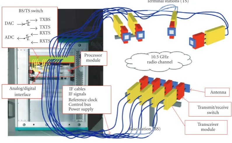
Figure1: System overview.
space division (SD) multiple access is implemented to en-able an efficient medium access in time, code, and space do-main. Equalization of frequency-selective MIMO channels is realized by joint detection in the uplink. Furthermore, we use joint-predistortion at the base station, which means that the data streams for the user terminals are pre-equalized at the base station. The required channel information for the equalization is obtained by channel estimation from uplink transmission. Regarding joint-predistortion, no additional signal processing for equalization at the user terminals is needed. But on the other side, the reciprocity of channel and transceiver and a constant channel between up- and down-link are required. The underlying system model of the digital hardware allows single- and multicarrier (OFDM) transmis-sion with the same digital hardware architecture [1]. For both transmission schemes, equalization is performed in the fre-quency domain. A cyclic burst transmission with a duration of 10.24 microseconds, as used in OFDM systems, simplifies signal processing in the frequency domain.
The choice of a radio frequency at 10.525 GHz is ad-dressed to future standards according to standard IEEE 802.16 covering a frequency range between 2 and 11 GHz. It seems likely that these higher frequency bands will become important for commercial use in future WLAN systems. In
Figure 1, the configuration of the SABA MIMO testbed is shown. The testbed supports up to eight transceiver modules. Each module includes a receive and transmit branch and an antenna switch with a calibration path. In the receiver part, the 10.525 GHz RF signal is down-converted to an intermedi-ate frequency of 175 MHz and in the transmit part the IF sig-nal is up-converted to the RF frequency. Each transceiver is equipped with a local oscillator being synchronized by a PLL using a 10 MHz reference signal. The transceiver modules are
connected to one central digital hardware platform by cables. The transmitter and the receiver are controlled by the central digital hardware. A short duration after a transmission be-gins, the receiver is started. The guard period and the dura-tion between transmission and recepdura-tion is dimensioned for typical WLAN indoor applications. Due to cyclic burst trans-mission and channel estimation, no further time synchro-nization techniques are required. Transmitter and receiver share one common clock, so no further frequency synchro-nization is needed. The TDD operation enables an alternat-ing use of receive and transmit branches in the base station and in the user terminals. This results in less effort and main-tenance of the testbed. Power supply for the transceivers, control bus, the intermediate IF signals, and the 10 MHz ref-erence signal are transmitted via cables. The maximal exten-sion of several 10 m is enough for investigation of indoor ap-plications. In future steps, the cables can be replaced by a car-rier and clock synchronization module.
The industrial PC rack in the left part ofFigure 1includes the digital signal processing, embedding a host PC which is connected to two carrier boards with FPGAs modules via cPCI interface. Together the two carrier boards provide eight slots for FPGA modules. Figure 2 shows one partition for a 4×4 system. The two BenADDA1 modules are equipped with 2 DA converter channels and 2 AD converter channels. The AD converters operate at a sample rate of 100 Msps with a resolution of 14 bits, which enables an undersampling of the 175 MHz IF signal. Furthermore, the module provides one FPGA and two memory blocks with a total storage ca-pacity of 8 MBytes. The digital transceivers include pulse
AD C AD C CLK DA C DA C AD C AD C CLK DA C DA
C 80-bit digital IO 80-bit digital IO
Transmit memory ZBT SRAM 32×512 kbit
100 MHz
Receive memory ZBT SRAM 32×512 kbit
100 MHz
Transmit memory ZBT SRAM 32×512 kbit
100 MHz
Receive memory ZBT SRAM 32×512 kbit
100 MHz
Receive memory ZBT SRAM 64×256 kbit 100 MHz
Program memory ZBT SRAM 64×256 kbit
100 MHz
ZBT SRAM 64×256 kbit 100 MHz Digital transceiver XC2V3000-5 FPGA Digital transceiver XC2V3000-5 FPGA Source/sink XC2V4000-4 FPGA Decoding/ encoding XC2V4000-4 FPGA SIMD/FFT processor XC2V6000-6 FPGA SIMD/FFT processor XC2V6000-6 FPGA Transmit memory ZBT SRAM 64×256 kbit 100 MHz BenADD A (ADD A 0) Dime II module Be nADD A (ADD A 1) Dime II module B en B lue II (Smal lBlue) Dime II module B en B lue II (Bi gBlue) Dime II module 8 serial status buses 10 serial control buses
2 RX + 2 TX channels (64 bits at 100MHz)
8 RX + 8 TX channels (128 bits at 100MHz)
8 RX + 8 TX channels (128 bits at 100MHz) 4 RX + 4 TX channels
(64 bits at 100MHz) Benera Dime II cPCI carrier board
User FPGA cPCI back plane cPCI host int erfac e
Figure2: Partition of BenERA carrier board.
shaping filters, cyclic extension, and digital up- and down-conversions. They are implemented on the FPGAs. The sym-bol rate in the baseband is 25 MHz. The BenBLUE II (Big-Blue) module is equipped with two Virtex II FPGAs from XILINX2and additional memory blocks (8 Mbytes), includ-ing the FFT and IFFT, as well as a highly parallel processor architecture to perform the algorithms in real time. With speedgrade −6, these modules provide a clock frequency up to 200 MHz. The architecture is described in detail in
Section 5.
The second BenBLUE module is used to realize channel coding, data generation, and evaluation. In this configura-tion, the second carrier board is not required but the mod-ular system enables flexibility and extensibility for future in-vestigations. The data rate between the modules on one car-rier board is 12.8 Gbits/s. The carcar-rier boards are connected via a back plane allowing a data rate of 6.4 Gbits/s.
The modulation for each data stream can be selected to BPSK, QPSK, 8-PSK, or 16- QAM. Spreading is realized by OVSF codes (orthogonal variable spreading factors) with spreading factors 1, 2, 4, 8, or 16. Training sequences enable necessary channel estimation.
3. INFLUENCE OF POLARIZATION ON CAPACITY
The channel capacity for different antenna configurations has also been examined [2]. For these investigations, based
2XILINX Inc., San Jose, Calif.
on indoor simulations using a ray-trace program developed in our institute, simple electric and magnetic dipoles have been used as shown on the right side ofFigure 3.
For every simulation, the antenna configurations shown on the right side of Figure 3 are the same for the trans-mit and the receive side. Main purpose of these investiga-tions was to compare the dual-polarized with the single-polarized antennas by analyzing the average channel capac-ity. InFigure 4, the advantage of dual-polarized antenna ar-rays is demonstrated. For single-polarized arar-rays, a distance of zero between the array elements does not exist, but for il-lustration this case is also depicted. In this simulated 2×2 MIMO channel, the ergodic capacity using dual-polarized elements at high-SNR range is higher than the capacity of the single-polarized antennas. Furthermore, for small aper-ture lengths, the gain in average channel capacity of the dual-polarized compared to the single-polarized configura-tion is higher than for greater aperture lengths. As depicted inFigure 4as well as in the left side ofFigure 3, the capacity of the dual-polarized antennas is independent of the overall aperture of the array. Increasing the number of antennas of both the base and the mobile station(s), as shown inFigure 3
6 5.5 5 4.5 4 3.5 3 2.5 2 1.5 1
M
ean
capacit
y
per
ant
enna
0 0.5 1 1.5 2 2.5 3 3.5 4 Antenna apertureL(wavelength)
2×2 dual-pol. 2×2 single-pol. 4×4 dual-pol., orthog. 4×4 dual-pol., parallel
4×4 single-pol. 6×6 dual-pol., orthog. 6×6 dual-pol., parallel 6×6 single-pol. (a)
Single-polarized array
· · ·
L
Dual-polarized array Electric dipole Magnetic dipole
L
L
L
(b)
Figure3: (a) Mean MIMO channel capacity per antenna element versus the overall aperture length of the array for an SNR=21 dB and (b) the different MIMO antenna arrays used in the simulations for the channels capacity.
the SABA testbed is designed with the option of using dual-polarized antennas.
4. ALGORITHMS
Signal processing for our testbed is based on block process-ing in the frequency domain. As already discussed, this al-lows for coexistence of OFDM and single-carrier transmis-sion with frequency-domain equalization (SC-FDE). Both schemes show strong similarities regarding performance and signal processing complexity. However, differences that exist between both transmission schemes can be analyzed and dis-cussed using our testbed. In the following, algorithms that are used for joint detection [3] of transmitted data in the uplink and joint-predistortion in the downlink [4] are pre-sented, starting with the fundamental system model.
In the following, lower-case letters are used for complex-valued scalars, lower-case boldface letters for complex-complex-valued vectors, and upper-case boldface letters for complex-valued matrices. We use (·)∗, (·)T, (·)H, E{·}, and tr{·}for
conju-gation, transposition, conjugate transposition, expectation, and trace of a matrix, respectively. The Kronecker matrix product is denoted by⊗. Then×nunit matrix is defined by the symbolIn. The notation [X]i,jrefers to the element in
theith row andjth column of a matrixX.
4.1. The system model
Since block processing for a multiuser MIMO system withK
single-antenna mobile stations and a base station deploying
Mantenna elements are assumed, for each of theK mobile
stations, a PSK or QAM symbol streamd(k) of lengthN is assigned, where the stacked overall symbol vector follows as
d=d(1)T,. . .,d(K)TT, d(k)=d(k) 1 ,. . .,d(Nk)
T . (1)
In the following, the covariance matrix of the data symbols is assumed asRd=E{ddH} =σd2IKN. That is, the data
sym-bols of each user are assumed to be temporally and spatially uncorrelated. For uplink and downlink transmission, the data symbols of all users are preprocessed before transmis-sion. For the uplink, this preprocessing depends on whether single-carrier transmission or OFDM is used. On the other hand, the transmit symbols also depend on the choice of a spreading scheme that might be used, but this scheme is not described in this section. During downlink transmission, the symbols that are to be transmitted additionally depend on the transmission channel which is used to design filter coef-ficients for downlink predistortion.
Next, a MIMO channel matrix betweenKuser antennas andMbase station antennas is defined in order to describe the relations between all transmit and all receive antennas. For the uplink, the channel matrix follows as
H= ⎡ ⎢ ⎢ ⎣
H(1,1) · · · H(1,K) ..
. . .. ...
H(M,1) · · · H(M,K) ⎤ ⎥ ⎥
⎦. (2)
11 10 9 8 7 6 5 4 3 2 1 0 Ergodic capacit y (bit/s/Hz) SNR
0 0.5 1 1.5 2 2.5 3 3.5 4 21 dB 18 dB 15 dB 12 dB 9 dB 6 dB 3 dB 0 dB
Distance between the elements (d/λ) Mean capacity of the dual-polarized elements Single-polarized antenna configuration
Figure4: Simulated ergodic capacity in bits per second per Hz of a 2×2 MIMO channel versus the overall aperture length of the array and the SNR at the receiver side.
functions. First, it prevents contamination of a block by in-tersymbol interference from the previous block. Second, it makes the received block appear to be periodic with period
N. Thus, the convolution of a data stream with a complex-valued channel impulse response (CIR)h(m,k)∈CWappears
to be circular, which is essential for the proper functioning of the FFT operation. Each of theN×Ndimensional subblocks
H(m,k)in (2) contains, therefore, the corresponding channel vectorh(m,k) in a circulant shape. For the downlink, trans-mission of a cyclic prefix of lengthW −1 before each data stream is also assumed. At the receiver side, the cyclic prefix is discarded.
The total system model and the receive vectorxthen fol-low for the uplink, for example, as
x=Hs+n. (3)
The transmit symbol vectorsis determined in the following sections. Equation (3) also contains a stacked noise vectorn. Noise is assumed temporally and spatially white through-out this paper, with zero mean and covariance matrixRn =
E{nnH} = σ2
ULIMN for the uplink and Rn = E{nnH} = σ2
DLIKNfor the downlink.
All transmission schemes that are examined in this paper require channel knowledge in the frequency domain. Using the Fourier matrixFN of dimensionN, with
FN
u,v=
1 √
Ne
−j(2π/N)(u−1)(v−1), (4)
the uplink channel matrix in the frequency domain follows as
ΔH=
IM⊗FN
HIK⊗F−N1
= ⎡ ⎢ ⎢ ⎣ FN . .. FN ⎤ ⎥ ⎥ ⎦ ⎡ ⎢ ⎢ ⎣
H(1,1) · · · H(1,K) ..
. . .. ...
H(M,1) · · · H(M,K) ⎤ ⎥ ⎥ ⎦ × ⎡ ⎢ ⎢ ⎣
F−1
N
. ..
F−1
N ⎤ ⎥ ⎥ ⎦= ⎡ ⎢ ⎢ ⎢ ⎣ Δ(1,1)
H · · · Δ(1,HK)
..
. . .. ...
Δ(M,1)
H · · · Δ(HM,K)
⎤ ⎥ ⎥ ⎥ ⎦. (5)
The resulting matrixΔH is of a blocked diagonal form,
that is, composed of diagonal submatrices. These diagonal submatricesΔ(Hm,k)in (5) contain the eigenvalues of the cir-culant channel submatricesH(m,k). For implementation, the Fourier matrix and its inverse are replaced by efficient FFT and IFFT algorithms, respectively.
For the downlink, the frequency-domain channel matrix follows asΔTH. That is, reciprocity between uplink and down-link channels is assumed. However, the transmission chan-nels also contain influence of transceivers in the base stations and the mobile stations, which, in general, results in nonre-ciprocal overall channels.
4.2. Joint detection in the uplink
4.2.1. Single-carrier transmission
For the single-carrier transmission scheme using frequency-domain equalization (SC-FDE), the uplink stacked transmit data vectorsjust follows as
s=d. (6)
Linear joint detection of theK symbol streamsd(k) in the frequency domain yields symbol estimates
d=IK⊗F−N1
WIM⊗FN
x, (7)
where the matrixWcontains receive filter coefficients. De-pending on whether zero forcing (ZF) or minimum mean square error (MMSE) optimization is applied,Wfollows as (see [5,6])
ZF :W=ΔH HΔH
−1
ΔH H,
MMSE :W=
ΔH HΔH+σ
2 UL σ2 d IKN −1 ΔH H. (8)
For efficient matrix inversion to be the fundamental part of the joint detection operation, there exist permutation matri-ces in order to transform the matrixΔHinto a block-diagonal
form withNblocks of dimensionM×K. For notational con-venience, the description of the permutation matrices is ne-glected at this point. Furthermore, note that joint detection in (7) and (8) only holds if the previously assumed covari-ance matrices Rd andRn are temporally white. The whole
H W d(1)=s(1)
d(K)=s(K)
n x(1)
x(M) FFT
FFT
IFFT
IFFT d(1)
d(K) . . . .
. . .
. .
Figure5: Single-carrier transmission system in the uplink.
As described in [5,6] for time-domain equalization, the zero-forcing-based equalizer yields unbiased symbol esti-mates, completely eliminating intersymbol interference (ISI) and multiple-access interference (MAI), and thus, contain-ing only the desired symbols and noise. The MMSE detector, however, leads to biased symbol estimates still containing ISI and MAI. These observations also hold for the frequency-domain equalizer described in this section.
4.2.2. OFDM transmission
Using OFDM transmission, all data symbols of each user are transmitted in parallel over N subcarriers. Compared to the previously described single-carrier transmission, only the IFFTs are shifted from the receiving base station to the transmitting mobile stations. The resulting data streams to be transmitted can be expressed as
s=IK⊗F−N1
d. (9)
Joint detection for OFDM follows as
d=WIM⊗FN
x. (10)
Here, the same ZF- or MMSE-based joint detection opera-tion as described for single-carrier transmission is applied, withWin (10) being defined in (8).
4.3. Joint predistortion in the downlink
4.3.1. Single-carrier transmission
To compensate for channel influence and to allow for spa-tial multiplexing while combating ISI and MAI already at the transmitter, joint-predistortion is applied at the transmitter. The stacked transmit data vectorsis then obtained as
s=IM⊗F−N1
βWIK⊗FN
d, (11)
where the matrixWcontains frequency-domain transmit fil-ter coefficients. The normalization factorβis used in order
to constrain the overall transmit energy Etr = E{sHs} to
Etr=NKσd2, where
β= Etr
σ2
dtr
WWH. (12)
Similar to time-domain predistortion in [7], either ZF- or Wiener-based optimization can be applied, whereWfollows as
ZF :W=Δ∗
H
ΔT HΔ∗H
−1 ,
Wiener :W=Δ∗
H
ΔT HΔ∗H+σ
2
DL σd2
IKN
−1
. (13)
Both approaches minimize the mean square error (MSE) under the constraint of constant transmit energy by using
β. The ZF solution additionally follows a zero forcing con-straint. Note that the Wiener approach requires knowledge at the base station of noise power at the terminals.
At the receiver, the symbol estimates directly follow as
d=β−1x (14)
with just compensating the received signals for power nor-malization at the transmitter usingβ.
Throughout this paper, uncorrelated data symbols and equal symbol powerσd2for all users is assumed. On the other
hand, uncorrelated noise is assumed at the receiving base station antenna elements in the uplink, as well as at the re-ceiving mobile stations during downlink transmission. Us-ing these two assumptions and, additionally, assumUs-ing equal noise power for up- and downlink withσUL2 =σDL2 , the
pre-distortion matrixW in (13) can be directly obtained from the uplink filter matrixWin (8) via transposition. Thus, no additional matrix inversion is necessary.
4.3.2. OFDM transmission
Linear predistortion in OFDM systems can be derived eas-ily from the preceding single-carrier concept by moving the FFTs from the transmitter to the receiver with
s=IM⊗F−N1
βWd. (15)
The same filter matrixWas in (13) and the same normaliza-tion factorβas in (12) can be used.
At the receiving mobile stations, the symbol estimates follow as
d=β−1I
K⊗FN
x. (16)
ADC receiverDigital
Source Channelcoding
FFT
Space-time signal processing
IFFT
Decoding
Digital transmitter
Sink
DAC Receive mode
Transmit mode
Receive mode Transmit mode Multicarrier
predistortion
Multicarrier equalization
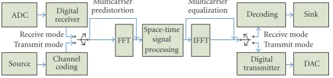
Figure6: Data flow of the digital signal processing at the base station.
Wiener approach is worse in high-SNR range than for the zero forcing approach. This is contrary to the MMSE filter in the uplink which always improves the system performance compared to zero forcing. However, when considering coded BER, the Wiener approach becomes always better than zero forcing because the few symbols that might exhibit low SNR due the Wiener filter can be corrected by using proper chan-nel coding. In an uncoded system, those symbols might be lost and cause the degradation of the Wiener filter compared to zero forcing.
In contrast to joint-predistortion for single-carrier trans-mission, in the OFDM-based system one can also normal-ize not only the mean transmit power of the whole block by usingβ, but also has access to each subcarrier to normal-ize the transmit power of each corresponding symbol sepa-rately. However, for this approach, theNnormalization fac-tors for all subcarriers need to be known at the receiving mo-bile stations in order to compensate for transmit normaliza-tion. This approach is not further considered for implemen-tation since erroneous estimation ofNnormalization factors additionally degrades system performance.
4.4. Extensions towards successive algorithms
For the uplink, detection ofK symbol streams can also be achieved successively. That is, symbols of one user are es-timated, quantized, fed back, and subtracted from the re-ceived signals. If quantization has been done correctly, the interference of this user is thus removed from the received signals so that the reliability of the succeedingly detected symbol streams increases. This concept is termed spatial decision-feedback equalization and is part of the well-known BLAST systems. The drawback consists in error propagation when symbols to be fed back are estimated wrongly. Suc-cessive joint detection is better suited to be implemented within OFDM systems rather than within SC-FDE, because for OFDM, quantization of already detected symbols, as well as feedback and feed forward filtering, take place in the fre-quency domain. Thus, there is no need for additional trans-formation between frequency and time domain as there is for SC-FDE.
For the downlink, successive predistortion is very similar to the uplink case. The downlink filter matrices can also, un-der some conditions that are discussed inSection 4.3.1, be di-rectly obtained from uplink filter matrices via transposition. However, the quantization operation is replaced in the down-link by a modulo operation, which periodically extends the
complex symbol plane in order to minimize transmit power. The drawback of this approach is symbol ambiguity due to the modulo operation.
In general, the main advantage concerning BER perfor-mance of both successive detection and successive predistor-tion is obtained in near-far scenarios where mobile terminals have different distances towards the base station. For exami-nation of coded BER, a straightforward approach consists in sequential processing of symbol estimation and channel cod-ing. That is, even for successive detection, symbols of all users are estimated before feeding this information to the chan-nel coding block. For more advanced signal processing, but which is also more complex, one can integrate channel cod-ing into each feedback loop of successive detection. This leads to an approach that is usually termed as turbo equalization.
4.5. Channel estimation
Channel estimation is achieved in the frequency domain by transmission of a preceding training block, followed by sev-eral data blocks. That is, each user transmits a cyclically ex-tended training block containing complex-valued random symbols that are known to both the transmitter and the re-ceiver. In the current real-time version of our testbed, train-ing blocks of different users/transmit antennas are transmit-ted sequentially. For a more efficient way of channel estima-tion, all training sequences can be transmitted at the same time, but over different subcarriers so that there is no inter-ference between the different training sequences. For this ap-proach one can exploit the finite length W of the channel impulse response. Due to this assumption, each transmitter needs to transmit training symbols only over each (N/W)th subcarrier and the channel transfer function of all subcarri-ers in between can be estimated via interpolation.
5. DIGITAL SIGNAL PROCESSING
5.1. Data flow
The system flow of the digital signal processing at the base station for the receive and transmit mode is shown in
Processor elements
Memory unit local data memory
Arithmetical unit MAC pipeline
Divider (1/x)
Common control unit Scaling factors
Addresses Control signals
Program memory External memory interface
In
te
rc
onnection
netw
or
k
TT T
Figure7: Schematic of the SIMD processor architecture.
the frequency domain. Afterwards a parallel signal proces-sor, which is described in detail inSection 5.2, performs the equalization algorithms. Regarding single-carrier (SC-FDE) transmission, symbol decision is realized in the time domain; therefore, the data has to be transformed back to the time do-main. In OFDM systems, symbol decision is made in the fre-quency domain; therefore, the data is routed directly to the sink.
Concerning OFDM transmission in the transmit mode, the symbols are available in the frequency domain and mitted directly to the processor. In SC-FDE, a Fourier trans-form is required before applying joint-predistortion in the frequency domain. The pre-equalized data streams are trans-formed back to the time domain before being forwarded to the digital transceiver.
For each transmission mode, the equalization is per-formed on the same digital hardware processor. Only the use of the FFTs and IFFTs is different. The redirection of the data flow is realized by multiplexer.
5.2. Parallel hardware architecture
The requirements for the signal processing can be derived from the used algorithms as described inSection 4. All algo-rithms are based on matrix operations: matrix inversion and multiplication. According to the used frequency-domain sys-tem model, groups of subcarriers can be calculated indepen-dently of each other in parallel. An efficient hardware archi-tecture should therefore be optimized for matrix and vector operations and should provide parallel processing.
In the SABA MIMO testbed, a software approach for the digital signal processing is implemented. The benefits are
(i) use of different algorithms, for example, MMSE, ZF, adaptive filters,
(ii) flexibility in matrix dimension, (iii) reduction of hardware complexity.
Furthermore, a novel highly parallel hardware architecture was developed to cope with the high computational burden.
The architecture is based on the SIMD (single instruction-multiple data) principle. As shown inFigure 7, up to thirty-two processor elements work in parallel and execute the same program. A daisy chain serves each processor element with data from the FFT/IFFT. Each processor element is equipped with a local memory unit to store the data streams as well as intermediate results during calculation. To serve the arith-metical unit, three read and one write accesses per cycle are required. Inside the arithmetical unit, a word length of 18 bits for real and imaginary parts of the complex values is used.
The arithmetical unit is optimized for vector operations and includes a MAC (multiply and accumulate) unit as well as a divider unit. The divider unit enables to calculate the reciprocal of a real value. This operation is required, for ex-ample, to normalize intermediate results. The number of di-visions in the considered algorithms is very small compared to the number of MAC operations. In this approach, eight processor elements share one divider unit. This leads to a re-duction of the amount of logic resources with a very small impact of run time in the used algorithms.
Some algorithms use information of adjacent frequency points, for example, frequency tracking or interpolation-based algorithms. This contradicts the SIMD principles. To also realize these algorithms on this hardware architecture, an interconnection network was implemented. This network is realized as a daisy chain, which means that each element is connected to the adjacent one.
One common control unit is used which operates on vec-tor commands. The unit executes the programs svec-tored in a separate program memory and generates the same control sequence for each processor element. A vector command has a size of 64 or 128 bits and includes the control sequence for the arithmetical unit and information to calculate address in-formation for vectors. The integrated address generator en-ables to calculate the addresses of a vector with up to 128 elements based on start address and a jumping width.
100
10−1
10−2
10−3
BER
(unc
o
ded)
6 7 8 9 10 11 12 13 14 15 16 17 18 Reserve parameter B
14–20 bit fixed-point arithmetic 64-bit floating-point arithmetic
Wmem=14
Wmem=16
Wmem=18
Wmem=20
Figure8: Comparison of floating-point versus fixed-point arith-metic using different word lengths.
complex multiplication per cycle. The accumulators for real and imaginary parts can optionally be preloaded with any value stored in the local memory.
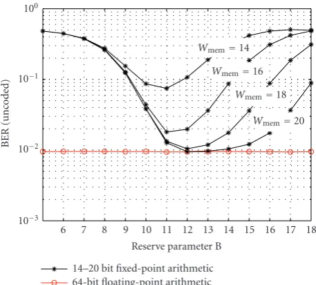
5.3. Fixed-point arithmetic
The whole architecture is based on fixed-point arithmetic. It is well known that fixed-point calculation causes under-and overflows during computation. Matrix inversion is also a problem in fixed-point arithmetic. To solve this problem, programmable scaling units are implemented on dedicated positions in the MAC and divider unit (e.g., between multi-plier and accumulator in the MAC unit). The units are de-signed as programmable shifters which cut offthe unused MSBs or LSBs. The shift length is defined in the program. Furthermore, simulations were made to investigate an opti-mum word length. InFigure 8, the estimated bit error ratio (BER) of a fixed point MMSE algorithm is compared with a floating point algorithm. The simulations are based on a worst case scenario using a system with eight receive anten-nas and seven transmit antenanten-nas. Moreover, correlation be-tween the antenna elements is assumed. The floating-point algorithm achieves a BER of 10−2assuming an SNR of 20 dB. The reserve parameter B indicates the parameter set for the scaling units. The parameter for each scaling unit in the com-puting chain can be derived from the reverse parameter B, which is not further discussed in this paper. As a result of
Figure 8, a word lengthWmemof 18 bits is required to achieve a BER comparable to the floating-point simulations.
6. ANALOG SIGNAL PROCESSING AND CONTROLLING
MIMO algorithms also affect the analog signal circuitry. Compared to SISO systems, there are higher requirements for linearity, dynamic range, LO phase noise, and return loss
suppression between antennas and transmitter outputs and receiver inputs, respectively. Some downlink predistortion schemes based on channel uplink matrix estimation require transceiver calibration in order to provide a reciprocal chan-nel matrix [8]. The large number of adjustable parameters, for example, uplink, downlink, calibration mode, attenua-tion, antenna polarizaattenua-tion, and the transceiver state moni-toring demands an efficient controlling procedure.
All RF circuits described below have been simulated and designed by common CAD tools and have been realized on soft substrates using SMD components.
Before the analog transceiver module is described in de-tail, the calibration concept is introduced.
6.1. Calibration concept
A very important issue that has to be considered in MIMO antenna systems is the calibration of the front-ends. It is known that for a bidirectional transmission, using downlink predistortion, the reciprocity of the channel has to be pro-vided. Front-end imperfections are the reasons for the non-reciprocity of the system.
The MIMO antenna system description uses an ideal transmission scattering matrix model in the frequency range such as that shown on the left side ofFigure 9with
bB bM
SBB SBM SMB SMM
aB aM
. (17)
In this case, the reciprocity of the channel is given if the fol-lowing conditions are fulfilled:
SBM=STMB, SBB=STBB, SMM=STMM. (18)
In (17), SBM andSMB represent the uplink and the
down-link channel matrix.SBB andSMM contain the matrices of
the reflection factors of the base and mobile station.aB,Mand bB,Mare the incoming and the outgoing waves at the base or
the mobile station. In a real channel, as depicted on the right side ofFigure 9, other effects like the mutual coupling of the
antennas and the transceiver mismatch influence the overall performance. Regarding these effects, the matricesSBMand SMBresult in [9]
SBM=ARBVSMBUTA TM,
SMB=ARMWSBMXTATB.
(19)
The diagonal matricesAXXcontain the amplifier coefficients
andV,UT,W,XT the antenna mismatching and coupling.
Using the following equations
V=I−SBBRRB
−1
, UT=I−RTMSMM
−1 ,
W=I−SMMRRM
−1
, XT=I−RTBSBB
−1 ,
(20)
where the diagonal matrices RXX comprehend the
Base station antennas
Mobile station antennas
aB,1
bB,1
aB,2
bB,2
bB,Mb
aB,Mb
aM,1
bM,1
aM,2
bM,2
aM,Mu
bM,Mu
MIMO-Kanal 1
2
Mb
1 2
Mu
SBM
SMB
Ideal channel
. . .
. . .
(a)
Mismatch: TX1 TX2
RX1 RX2
C
o
upling
Transmit Receive
Real channel
(b)
Figure9: (a) Scattering matrix representation of an ideal MIMO channel and (b) the additional influences such as transceiver mismatch and antenna coupling.
(1) Minimizing the matrices Sy y andRxx within V, U
T,
W, andXT. This requires a very good matching of the
transmit/receive (TR) modules and the antennas, de-pending on the antenna coupling.
(2) Equalizing the responses of the transmitters and re-ceivers to Dirac pulses.
The calibration consists of two parts. The first one is a wideband off-line calibration which is used to compensate the influence of the passive elements, the DA converter, the nonideal transformers, and the IF filter on the signal process-ing side. The other part is a narrowband on-line calibration of the active components which are causing changes in phase and amplitude of the signals during operation. To perform these two calibration schemes with sufficient accuracy, cer-tain hardware requirements have to be met.
A real MIMO system was modeled and simulated us-ing the scatterus-ing matrix form introduced above.Figure 10
shows the results of these simulations which are based on an indoor scenario at a frequency of 10.5 GHz. The number of the base and mobile station antennas is 8 and 4. The modu-lation used is QPSK. For a 1 dB degradation at a BER of 10−3 in comparison to an ideally calibrated and matched system, the unbalance of the magnitude must be lower than 1.4 dB and the unbalance of the phase lower than 10◦ between all transceivers. The transceiver return loss should be lower than −3 dB and the antenna matching and coupling should both be lower than−10 dB.
To perform 16 QAM modulation, the requirements for reciprocity increase.
6.2. Block diagram of the transceiver
The block diagram of Figure 11 gives an overview of the analog signal processing of a transceiver. Each transceiver of our demonstrator consists of filters, amplifiers, controlled attenuation circuits, mixers, LO frequency processing, volt-age/current supply, sensors, and control and surveillance circuits.
For calibration purposes, each transceiver is provided with a reciprocal third channel. This signal path has an
indi-vidually measured and recorded transmission behavior. Dur-ing calibration mode, it helps to supply the receiver input or to clean up the transmitter output via the combined an-tenna/calibration switch.
Only one analog frequency conversion is employed, re-sulting in less effort for LO generation and smaller number of components (e.g., filters and mixers). The corresponding larger filter losses (5–8 dB) can easily be compensated by low-cost amplifiers at low-power levels. In contrary to the com-monly implemented complex I-Q conversion using two A/D converters, the present concept utilizes subsampling conver-sion, so that problems with mixer and I-Q imbalance can be avoided. After the A/D conversion, a digital signal of about 30 MHz bandwidth with a resolution of nominal 14 bits is available, which is further shifted down to the complex base-band. The same principle in reverse direction is used for the transmitter.
All transceivers must be supplied with a common phase-locked oscillator signal. Base station transceivers at higher frequencies should have short connections to the anten-nas, otherwise these may have distances of several to many wavelengths from one to each other. Moreover terminal transceivers should have the same architecture as the base station transceivers. Therefore it is advisable to generate the local oscillator signal on the transceiver board. To lock the phase of the LOs, a 10 MHz reference signal is used, which is generated in a low-noise TCXO in the centralized hardware and is distributed via cables. The output of the 10 GHz VCO is amplified and distributed to the three fre-quency converters of the transmitter, receiver, and calibration path.
100
10−2
10−4
10−6
Un
co
d
ed
B
E
R
−20 −10 0 10 20
Eb/N0(dB)
r= −1 dB
r= −2 dB
r= −3 dB
r= −6 dB
r= −12 dB Ideal match (a)
100
10−2
10−4
10−6
Un
co
d
ed
B
E
R
−20 −10 0 10 20
Eb/N0(dB)
r= −1 dB
r= −2 dB
r= −3 dB
r= −6 dB
r= −12 dB Ideal match (b)
100
10−2
10−4
10−6
Un
co
d
ed
B
E
R
−15 −10 −5 0 5 10
Eb/N0(dB)
Δmag= −3 dB
Δmag= −6 dB
Δmag= −9 dB
Δmag= −12 dB
Δmag= −15 dB Ideal calibration (c)
100
10−2
10−4
10−6
Un
co
d
ed
B
E
R
−15 −10 −5 0 5 10
Eb/N0(dB)
Δph=40◦
Δph=30◦
Δph=20◦
Δph=10◦ Ideal calibration (d)
Figure10: Simulation of the impact of erroneous calibration and antenna mismatching on the BER for QPSK. Antenna matching is equal to (a)−3dB and (b)−10dB. Calibration errors are illustrated in (c) magnitude and (d) phase.
Due to the calibration requirements, all transceivers should behave in the same manner in case of fluctuation of the power supply, temperature, and the variation of the used elements. To guarantee a stable operating point of the am-plifiers, stabilizing circuits with mounted sensors are used. The adjustment of the operation point of these amplifiers can also be performed manually. Furthermore, these circuits are able to warn if any component is not working properly. The maximum transmitter output power is 20 dBm for linear op-erations, realized in five amplification stages. The minimum
receiver input sensitivity is−83 dBm and is amplified by six stages up to +6 dBm. The noise figure of the receivers is about 1 dB.
6.2.1. Attenuators
−20 dB
HPA 3 Attenuator 2 HPA 1 RF filter HPA 2 10 525 MHz
Mixer
Attenuator 1 IF amplifier 4
MUX TX multiplexer 2
REF multiplexer
−
VC
C
1
+V
CC
2
+V
CC
1
10
MHz
Attenuator 3
Attenuator 4
Mixer
1 : 3 10 350 MHz
f /8 PLL
HPA MRVCO
1 : 2 MUX
MUX Attenuator 1 IF amplifier 1 RX
multiplexer 2
Bu
s
LNA 1 Attenuator LNA 2 RF filter LNA 3 Mixer 10 525 MHz
a
a
a
a
175 MHz
a a TR module
Figure11: Block diagram of the transceiver module.
together covering an attenuation range of about 70 dB with a 1 dB resolution. These attenuators consist of analog and pas-sive components, which are digitally adjusted to a certain at-tenuation value. Another requirement of these components is a short switch time. The reaction of the digital controlling and analog attenuation circuit must be quite small, which means smaller than the guard period of the used chip.
The attenuators at RF have to realize attenuation steps of about 0, 20, and 40 dB. These values are allowed to have large tolerances of several dB. However, they should be constant within one calibration period. As no precise attenuation val-ues are required, the circuit of Figure 12has been chosen, which is distinguished by a very simple structure using only four PIN diodes for the required three stages. The PIN diodes are connected between the microstrip transmission lines and the stubs, marked with the numbers 1 to 4 in the layout. The achieved attenuations are about 1, 22, and 42 dB with return losses at both ports better than 20 dB at all stages.
6.2.2. Antenna and calibration switches
Because the transmission scheme is based on TDD, the an-tennas must be connected alternately to the receiver input and to the transmitter output. They are designed similarly to the attenuator circuits and are digitally controlled as well. For the calibration mode, the switch has to provide a fur-ther port, serving as an input or output for the calibration RF signal. The specifications of this four-port component re-sult from the following requirements: low insertion loss in
1 2
3 4 Attenuator circuit
10 525 MHz,0, -20, -40 dB, IHF September 2004
Figure12: Layout of an attenuator circuit for 10.5 GHz with diff er-ent attenuation stages (0 dB, 20 dB, and 40 dB).
Tr
an
sm
it
te
r
Re
ce
iv
er
Antenna Calibration port
Antenna switch IHF
Figure13: The calibration switch with attenuator circuits.
a short circuit in various places of the circuits, to realize the different operation states of the switch.
6.2.3. Control units, system monitoring, and power supply
A microcontroller is used to survey and control the trans-ceivers. The microcontrollers are nowadays not only low-cost and very small elements, but also easily programmable and very fast. The used microcontroller is able to both handle all mnemonic codes and perform an 8×8 multiplication during one cycle of 100 nanoseconds. The program memory is based on FLASH-ROM so that the code can be reprogrammed on demand without any need to change the circuit. In the microcontroller, a multichannel A/D-D/A converter and an EUSART (enhanced universal synchronous asynchronous re-ceiver transmitter) are integrated. Different states can be read and monitored through the analog interface and the sen-sor values, for example, the output power or the fluctua-tions of the operating voltage can be evaluated and processed. EUSART is a free programmable serial interface unit which enables data transfer to the FPGA. The microcontroller re-ceives the control information by this fast bidirectional se-rial interface from the FPGA and gives surveillance informa-tion through a feedback channel over the same interface as before to the FPGA. This makes the FPGA able to supply each transceiver independently with control data. Some of the control information are listed below:
(i) operating state (down- or uplink, calibration mode), (ii) current attenuation value of the transmitter or the
re-ceiver branch,
(iii) polarization state of the antenna,
(iv) data delays of the cables used for synchronization and equalization in all switch states.
The surveillance information of the transceivers includes, for example,
(i) the currently transmitted power of the antenna, (ii) malfunction of circuit components,
(iii) fluctuations of the operating voltage, (iv) the current state of the switching circuits,
(v) data failure in the system.
Figure14: A transceiver branch manufactured to work at 10.5 GHz.
The serial data channels are realized by using two coaxial ca-bles, each cable for one direction. The data rate is 10 Mbits/s for each direction and is quite the same as in the RS232 pro-tocol. In these coaxial connections the IF signals for both directions (up- and downlink) are also added. The IF sig-nal is a passband sigsig-nal of fIF =175 MHz and a bandwidth of fBW = 30 MHz. The serial control information on the other hand are lowpass signals with a cut-offfrequency of 100 MHz. They can be distinguished from the IF signals by filtering. In the microcontroller, additional functions have also been implemented to simplify the off-line or the on-line calibration. The microcontroller is able to check for every state which is needed to perform a calibration, thus making the electrical measurement of the transceivers more conve-nient.
The power supply of the transceivers is implemented by means of DC/DC converters. They work with only one in-put voltage value to create more than one high-power outin-put voltage state. Some of the advantages of such a circuit are that it does not need a negative input voltage and that even high fluctuations of the input voltage do not affect the power dis-sipation. In general the power dissipation of such circuits is much lower than in circuits with linear controllers and the surveillance of the output power can be performed in more convenient ways. Instead of using a common two-wire line, we use a coaxial cable both for supplying the input voltage and the fref=10 MHz reference frequency. A filter is used to separate the reference frequency from DC.
6.3. Realization of RF components
the previous circuits to the final amplifier stage, which is also balanced. At the end of the circuit, a coupler can monitor the transmission power.
7. SUMMARY AND OUTLOOK
In this paper, the real-time MIMO testbed SABA has been presented. A system concept has been described to perform equalization algorithms in the frequency domain. The digital signal processing is based on a novel highly parallel processor architecture using the SIMD principle to compute these al-gorithms in real time. Furthermore, the architecture enables single-carrier and OFDM transmission on the same hard-ware platform. A MIMO specific calibration concept is pre-sented and the concept and design of the analog hardware is described.
The 25 MHz RF bandwidth is divided into 256 sub-carriers. Regarding 16- QAM modulation, each data stream achieves a raw data rate of 100 Mbits/s. The carrier frequency of 10.525 GHz and the exploitation of multipath fading tar-gets typical WLAN applications.
Using this testbed, future transmission schemes for spa-tial multiplexing and multiuser systems can be tested and evaluated. Due to bidirectional transmission, uplink channel knowledge can be reused for downlink predistortion. Thus, among different transmission schemes, the promising ap-proach of predistortion can be tested under realistic condi-tions.
The testbed is still under development. Currently, the sys-tem consists of two transmitters and two receivers enabling joint detection of two spatially multiplexed data streams. Joint-predistortion can be currently used only for the same transmission direction because the switch and the control-ling part for bidirectional transmission are still in progress. However, first performance measurements result in an aver-age uncoded BER of 10−2for 16- QAM transmission at 25 dB SNR.
In the next step, the system will be extended to 2×2 bidi-rectional transmission and after that to a 4×4 MIMO sys-tem. Furthermore, channel coding algorithms will be imple-mented.
Since the transmission quality varies with channel, adap-tively choosing between spatial multiplexing and conven-tional orthogonal transmission schemes as, for example, TDMA is desirable. Therefore, the physical layer provided by our MIMO testbed will be combined with an adaptive MAC layer. The MAC layer functionality will be implemented in the existing FPGA system and will provide real-time capabil-ity. The hardware platform for the MAC layer will be a FPGA module with two embedded PowerPCs on board. This exten-sion is granted by the German Research Foundation (DFG).
REFERENCES
[1] L. Br¨uhl and B. Rembold, “Comparison of signal processing for spatio-temporal multi-user equalization in multi- and single-carrier CDMA systems,” inProceedings of 2nd Karlsruhe
Work-shop on Software Radios (WSR ’02), Karlsruhe, Germany, March
2002.
[2] C. Oikonomopoulos-Zachos and W. Keusgen, “Increasing the capacity of MIMO antenna systems when using Orthogonal Po-larized antennas,” inProceedings of European Microwave Week
2003 (EuMW ’03), Munich, Germany, October 2003.
[3] C. Degen and L. Br¨uhl, “Multi-user detection in OFDM systems using CDMA and multiple antennas,”European Transactions on
Telecommunications, vol. 14, no. 6, pp. 481–490, 2003.
[4] C. Degen and L. Br¨uhl, “On linear predistortion techniques for single-carrier and OFDM SD/CDMA systems,” inProceedings of 15th IEEE International Symposium on Personal, Indoor and
Mobile Radio Communications (PIMRC ’04), vol. 2, pp. 1501–
1505, Barcelona, Spain, September 2004.
[5] A. D. Wahlen, Detection of Signals in Noise, Academic Press, New York, NY, USA, 1971.
[6] A. Klein, G. K. Kaleh, and P. W. Baier, “Zero forcing and min-imum mean-square-error equalization for multiuser detection in code-division multiple-access channels,”IEEE Transactions
on Vehicular Technology, vol. 45, no. 2, pp. 276–287, 1996.
[7] M. Joham, K. Kusume, M. H. Gzara, W. Utschick, and J. A. Nossek, “Transmit Wiener filter for the downlink of TDD DS-CDMA systems,” inProceedings of 7th IEEE International Symposium on Spread Spectrum Techniques and Applications
(ISSSTA ’02), vol. 1, pp. 9–13, Prague, Czech Republic,
Septem-ber 2002.
[8] C. Degen, O. Koch, W. Keusgen, and B. Rembold, “Evaluation of MIMO systems with respect to front-end imperfections,”
inProceedings of 11th European Wireless Conference (EW ’05),
Nicosia, Cyprus, April 2005.
[9] L. Br¨uhl, C. Degen, W. Keusgen, B. Rembold, and C. M. Walke, “Investigation of front-end requirements for MIMO systems using downlink pre-distortion,” inProceedings of 5th European
Personal Mobile Communications Conference (EPMCC ’03),
Glasgow, Scotland, UK, April 2003.
Daniel Borkowskiwas born in Germany in 1975. In 2003, he received the Dipl.-Ing. degree in electrical engineering from the RWTH Aachen University. Ever since, he has been a Research Assistant in the Insti-tute of High Frequency Technology, RWTH Aachen University. His work is focused on the digital signal processing for high data rate communication systems. He is inter-ested in MIMO and SDMA systems and their realization in real-time applications.
Lars Br¨uhl received the Dipl.-Ing. (M.S. E.E.) and Dr.-Ing. (Ph.D.E.E.) degrees from RWTH Aachen University, Germany, in 1997 and 2005. From 1998 to 2004, he was a Research Assistant with the Insti-tute of High Frequency Technology, RWTH Aachen University. His research activities mainly focus on digital signal processing and processor design for multiple-input multiple-output (MIMO) communication
Christoph Degen was born in Germany in 1976. He received the Dipl.-Ing. de-gree in electrical engineering from RWTH Aachen University, Germany, in 2000. Cur-rently, he is a Research Assistant in the Insti-tute of High Frequency Technology, RWTH Aachen University, where he is working to-wards the doctorate degree (Ph.D.). His research interests include space-time sig-nal processing with emphasis on OFDM
transmission and frequency-domain equalization for single-carrier transmission.
Wilhem Keusgenreceived the Dipl.-Ing. (M.S.E.E.) and Dr.-Ing. (Ph.D.E.E.) degrees from the RWTH Aachen University, Aachen, Germany, in 1999 and 2005, respectively. From 1999 to 2004, he was with the Institute of High Frequency Technology, RWTH Aachen University, as a Research Assistant. His research activities mainly focus on multiple antenna systems, microwave front-end technolo-gies and microwave antennas. In 2004, he joined the Fraunhofer Institut f¨ur Nachrichtentechnik, Heinrich Hertz Institut, Berlin, where he is working on the implementation of broadband mobile communication systems.
Gholamreza Alirezaei was born in Esfa-han, Iran, in 1976. In 2001 he received the Dipl.-Ing. degree in electrical engineering from the RWTH Aachen University, Ger-many. Currently, he is a Research Assistant in the Institute of High Frequency Technol-ogy, RWTH Aachen University. His research interests are front-end circuits for MIMO systems as well as digital modulation clas-sification and blind estimation.
Frank Geschewski received his Dipl.-Ing. degree in electrical engineering from RWTH Aachen University, in 2001. Since Septem-ber 2001, he has been working as a Research Assistant in the Institute of High Frequency Technology, RWTH Aachen University. His research is focused on planar microwave an-tennas as well as simulation and design of microwave components and devices.
Christos Oikonomopoulos was born in Greece in 1976. He studied electrical en-gineering at the RWTH Aachen University and received the Dipl.-Ing. degree in 2003. Since January 2003, he has been a Research Assistant in the Institute of High Frequency Technology, RWTH Aachen University. He is working towards his Ph.D. degree He is interested in the investigation of antennas for MIMO applications, capacity of MIMO channels, and microwave circuits.
Bernhard Remboldreceived the Dipl.-Ing. and Dr.-Ing. degrees in electrical engineer-ing from the Technische Hochschule Darm-stadt in 1969 and 1974. In 1975, he joined the AEG-Telefunken, Ulm, were he was in-volved in the development of mm-wave components and subsystems. He became Leader of the group in the same year. In May 1984, he went to Telefunken-Sendertechnik, Berlin, a former division of the same