Antenna-Coupled mm- Wave Electro-Opt ic Modulators and
Linearized Electro-Optic Modulators Thesis by
Finbar T. Sheehy
In Partial Fulfillment of the Requirements
for the Degree of
Doctor of Philosophy
California Institute of Technology
Pasadena, California
1993
To the Memory of
John Alphonsus Sheehy (1934 - 1990)
my father,
who believed in me
though I did not, supported me when I did,
and laughed with me
at our "failures."
I thank Professor William B. Bridges, my thesis advisor. During my time at Caltech he has provided me with much useful advice and many fascinating insights, in areas by no means limited to the work presented here. I have come to realize how fortunate I am to have had an advisor with a genuine interest in my personal as well as professional development, a man available to me as teacher, mentor and friend. I very much appreciate his guidance and support.
I would also like to thank James H. Schaffner, at Hughes Research Laboratories, who collaborated with us on this project, building devices, providing technical information, and taking part in many invaluable technical discussions. I thank Professor David B. Rutledge for his technical advice, which has been often sought and freely given.
I have enjoyed working with everyone involved in Professor Bridges' group. Reynold Johnson provided friendly and practical technical help, always with a sense of humor and fun. Laura Rodriguez and Connie Rodriguez, Dr. Bridges' secretaries, have cheerfully navigated the clerical complexities of Caltech for me. Professor Bridges' other research students, Yongfang Zhang, Lee Burrows, and Arthur Sheiman, provided much support, encouragement and ideas. Arthur deserves special mention for his expertise in keeping my car on the road for so long.
v
which provided me with most of my financial support during this project, and to Schlumberger, whose fellowship program supported me for my first year at Caltech. Financial support of the project was provided primarily by Rome Laboratories, who also provided my summer support. In addition, the project received support from the Caltech President's Fund.
I have enjoyed the support of many friends, inside and outside Caltech, who have encouraged me during my time here. That my experience of graduate school has been so much fun is largely due to them, and I thank them all, especially Barry Ryan.
vi Abstract
We have demonstrated antenna-coupled electro-optic modulators a t frequencies up to 98 GHz. The antenna-coupled design allows the modulator to overcome the velocity-mismatch problem which limits the maximum operating frequency of more conventional designs. Several modulators have been demonstrated, including a prototype narrowband phase modulator (optical wavelength 0.633 pm) at 10 GHz, a narrowband phase modulator (0.633 pm) at 60 GHz, a broadband Mach-Zehnder modulator operated as a phase modulator at 60 GHz, and a broadband Mach-Zehnder amplitude modulator at 94 GHz (optical wavelength 1.3 pm). The performance of the prototype modulator at 10 GHz is not quite as good as that of conventional modulators at this frequency, but is comparable. The performance of the mm-wave modulators cannot be directly compared to conventional modulators, as none exist at these frequencies. However, we have established that the relative performance of the mm-wave modulators is consistent wit,h a simple scaling law.
vii Contents
Page
1. Introduction 1.1 The Field
1.2 The Thesis
1.3 Brief Review of the Technology
1.4 The Antenna-Coupled Modulator Project
1.5 The Highly-Linear Modulator Study
2. The Physics of Electro-Optic Modulators 2.1 The Electro-Optic Effect
2.2 Electro-Optic Phase Modulation
2.3 Lumped-Element elect so-Optic Phase Modulators 2.4 The Traveling-Wave Phase Modulator
2.5 Frequency Response of the Traveling-Wave Phase Modulator
2.6 The Mach-Zehnder Amplitude Modulator
2.7 The A/? Coupler-Modulator 2.8 Theory of Coupled Modes
2.9 Directional Coupling
2.10 The A/? Coupler-Modulator Analysis in Practice
2.11 The Frequency Response of a Traveling-Wave
.
.
.
V l l l3. The Antenna-Coupled Modulator Concept
4. Antenna-Coupled Modulators - Theoretical Considerations 4.1 Antennas on a Dielectric Half-Space
4.2 Modulation Efficiency as a Function of the Number of Antennas 4.3 Modulator Beamwidth and Phasefront Curvature
4.4 Feed Design
5. Antenna-Coupled Phase Modulator at 10 GHz
5.1 Design of the Prototype Modulator 5.2 Theoretical Model of the Modulator 5.3 Fabry-Perot Measurement Technique 5.4 Experimental Setup
5.5 Experimental Results
5.6 Comparison of Experimental and Theoretical Frequency Response
5.7 Comparison of Peak Performance with that of Conventional Modulators
5.8 Conclusion
6. Ant enna-Coupled Millimeter- Wave Modulators
6.1 Design of the Narrowband 60 GHz Phase Modulator
6.2 Design of the Broadband 60 & 94 GHz Amplitude Modulators 6.3 Study of Phasefront Curvature in Scale Model of Feed
6.4 Experimental Setup
ix
6.6 Narrowband Phase Modulator Results at 60 GHz
6.7 Broadband Modulator Results a t 60 GHz
6.8 Broadband Modulator Results at 94 GHz
6.9 Design of the 94 GHz Ap Coupler-Modulator 6.10 Conclusions
7. Design and Implementation of Linearized A/? Electro-Optic Modulators - A Theoretical Study
7.1 Introduction
7.2 Cascade Linearization of Ap Modulators 7.3 The Splitter/Combiner Networks
7.4 Design of a Linearized A p Modulator
7.5 Practical Implementation of the Spli tter/Combiner Networks
7.6 Design Examples
7.7 Conclusion
8. Comparison of mm- Wave Electro-Optic Transmission Systems 8.1 Introduction
8.2 Performance of System Components
8.2.1 Modulator Performance
8.2.2 Detector Performance
8.2.3 Diode Mixer Performance
8.2.4 Electro-Optic Mixer Performance
8.3 Analysis of System Performance
8.3.1 Performance of Conventional
X
8.3.2 Modulate-Mix-Detect System
8.3.3 Modulate-Mix-Detect with Mode-Locked Laser
8.3.4 Mix-Amplify-Modulate-Detect System
8.3.5 System Performance Summary
8.4 Practical Considerations
9. Broadband Substrate-Wave-Coupled Electro-Optic Modulator 9.1 Introduction
9.2 The Proposed New Structure
Appendix A
Radiation Pat tern of the Interfacial Antenna
A l . Introduction 159
A2. The Interfacial Antenna 159
A3. Computation of Ei0(0,4) and Ei4(B,$) for a V-Antenna 164
A4. Special Case: Dipole in Free Space 168
A5. Special Case: V-Antenna in Free Space 169
A6. Special Case: Infinitesimal Dipole on a Dielectric Half-Space 172
A7. V- Antenna on a Dielectric Half-Space 173
xi
Appendix I3
Optimum Power Distribution in Traveling- Wave Electro-Optic Modulators
B1. Abstract
B2. Introduction
B3. How to Split a Traveling-Wave Modulator
B4. The Definitions
B5. Ideal Modulator Segments
B6. Lengt h-Limited Modulator Segments
B7. Loss-Limited Modulator Segments
B8. Optimum Lengths - Velocity Mismatch Case
B9. Frequency Response Effects - Velocity Mismatch Result
B10. Frequency Effects - Loss Lirnited Result
B11. Other Configurations
B12. Conclusion
Appendix C
Fabrication of the Electro-Opt ic Modulators C1. Introduction
C2. Optical Waveguide Fabrication
C3. Mask Design and Production
C4. Buffer Layer and Electrode Deposition
xii Appendix D
Frequency Content of Mixed Phase-Amplitude Modulation D l . Introduction
D2. Optical Transfer Function of the Modulator
D3. Frequency-Content Analysis for Mixed Modulation
D4. Analysis Performed for a Mach-Zehnder
Amplitude Modulator
D4.1 Balanced Mach-Zehnder Amplitude Modulator
D4.2 Single-Sided Mach-Zehnder Amplitude Modulator
D5. Analysis of a Ap Coupler-Modulator
Appendix E
Analysis of the Linearized Modulators E l . Introduction
E2. Two-Tone Dynamic Range
E3. Computation of Dynamic Range
1
1. Introduction
1.1 The Field
Optical technology is becoming increasingly important for communications and measurement. Researchers have developed a wide variety of devices which allow light to interact with electrical signals (or other optical signals). These include lasers, switches and switching networks, amplifiers, detectors, and various types of modulators. There are many applications, including analog links [I], digital links 12 - 51, and other more specialized applications such as optical wavefront measurements [6].
1.2 The Thesis
This thesis reports on two developments of optical rnodulators using the electro- optic effect in LiNb03. In elect so-optic materials the refractive index (or, equivalently, the dielectric constant) is a function of the electric field strength, and this effect can be used in a variety of ways to produce optical modulators. The developments reported are high-frequency modulators, with demonstrated operation at up to 98 GHz in the laboratory, and theoretical studies of highly linear modulators and a variety of possible electro-optic links.
1.3 Brief Review of the Technology
material relatively cheap. Titanium in-diffusion is the most common method of
producing the optical guides, and was demonstrated in 1974 (Schmidt and
Kaminow [9]). Other optical waveguide production techniques include proton exchange (Jackel et al. [lo]) and ion implantation (Destefanis et al. [Ill). The
major competitors to LiNb03 in modulators are semiconductors such as GaAs,
InP, and InGaAsP [l2], which have support from the huge existing efforts in
semiconductor development, and possible compatibility with solid-state laser
fabrication methods. To date, however, the optical losses are higher in these
modulators than in LiNb03 and it is not yet clear which material will be
favored in the future, or whether other preferred materials will emerge.
Electro-optic modulators, of course, involve interaction between electrical and
optical signals. In order to achieve efficient interaction, it is necessary to
confine both the optical and electrical signals. The optical signal is confined by
the optical waveguide just below the surface of the electro-optic material. In a
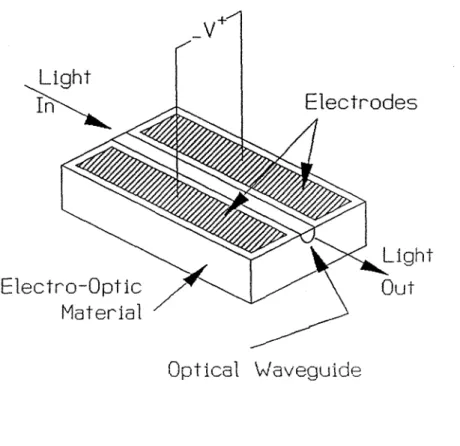
single-waveguide phase modulator (Figure 1.1) the electrical signal is impressed
upon the optical signal by positioning electrodes so as to produce the desired
electric field across the optical waveguide, modifying the propagation conditions
there. Alternatively, two coupled optical waveguides may be used in a directional-coupler configuration. By controlling the refractive index of the
waveguides, it is possible to change the coupling so that an arbitrary amount of
the input power is transfered to the coupled port [13]. This electrically-
controlled optical switch may be an amplitude modulator if only one of the
Opt
leal
Waveguide
Figure
1.1
Elec-tro-Optic
Phase
Modulator
Optical waveguide confines optical beam to high-electric-field region between the
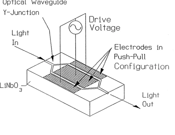
wavelength longer than the other. The light is phase-modulated in opposite
senses in the two paths, then recombined in a second 3 dB coupler (Figure 1.2). This produces an amplitude-modulated output by virtue of the controlled
constructive or destructive interference between the outputs of the two paths.
LiNbOQ does have some undesirable attributes. It is anisotropic, but more
important, it is dispersive. Its refractive index to microwaves is much higher
than to light. The result is that microwave and millimeter-wave signals travel
too slowly along the interaction electrode structure to interact properly with the
light in the optical waveguide below. This gives rise to a sensitivity-bandwidth
tradeoff of 6dB/octave for baseband modulators. In addition, attenuation of the
modulating signal in the electrode structure becomes a problem as the signal
frequency rises. Finally, it becomes very difficult to make connections to the
modulator in the electrical domain at high frequencies, because lead and
connector parasitics may be severe [15].
1.4 The Antenna-Coupled Modulator Project
In the antenna-coupled modulator project we examined a new approach to the
design of electro-optic modulators on LiNb03. This approach produces a
sensitive modulator which can operate at high (mm-wave) modulation
frequencies. The resulting modulator cannot have a baseband response, but
rather will show bandpass behavior. For this reason it is not suitable for digital
transmission, which requires baseband response, but is suitable for analog
applications where bandpass behavior is a,cceptable. Bandpass modulators for
high frequencies have been proposed and demonstrated by others [16,17], but in
Optical Waveguide
Y-Junction
Light
Electrodes in
Figure
1.2
Mach-Zehnder Amplitude Modulator
Optical beam i s s p l i t into two paths. The paths a r e phase-modulated with o p p o s i t e polarfties and
and is subject to large parasitic effects and high conductor losses as before. In
our design, the cable parasitics are removed, and conductor losses are less
significant.
1.5 The Highly-Linear Modulator Study
In the highly-linear modulator study we looked at ways of modifying a Ap
directional-coupler modulator to improve the linearity of its transfer function
(IOut/Vin). This type of modulator has a sinc2 transfer function in its
unmodified form, and is operated at the inflection-point of the transfer function,
where the second-harmonic distortion is zero. Third-order intermodulation is
appreciable, however. We have found that it should be possible to construct a
modulator which, when properly biased, has virtually no products of second-,
third- or fourth- (and possibly fifth- or sixth-) order in its output.
References
[I] C.H. Cox 111, G.E. Betts, and L.M. Johnson, "An Analytic and Experimental Comparison of Direct and External Modulation in Analog Fiber-
Optic Links," IEEE Trans. Microwave Theory & Tech., Vol. 38, No. 5 , May
1990
[2] S.K. Korotky, et al., "4-Gbit/s Transmission Experiment over 117 km of Optical Fiber Using a Ti:LiNb03 External Modulator," IEEE J . Lightwave
Tech., Vol. 3, No. 5, October 1985
Talrnan, and A.R. McCormick, "&Gbit/s Transmission Experiment over 68 km
of Optical Fiber using a Ti:LiNb03 External Modulator," IEEE J. Lightwave Tech., Vol. 5, No. 10, October 1987
[4] E.J. Murphy, J. Ocenasek, C.R. Sandahl, R.J. Lisco, and Y.C. Chen,
c L
Simultaneous Single-Fiber Transmission of Video and Bidirectional
Voice/Data Using LiNb03 Guided Wave Devices," IEEE J. Lightwave Tech., Vol. 6, No. 6, June 1988
[5] T. Okiyama, H. Nishimoto, I. Yokota, and T. Touge, "Evaluation of 4-Gb/s Optical Fiber Transmission Distance with Direct and External Modulation,"
IEEE J . Lightwave Tech.,Vol. 6, No. 11, November 1988
[6] R.H. Rediker, T.A. Lind, and B.E. Burke, "Optical Wavefront
Measurement and/or Modification using Integrated Optics," IEEE J.
Lightwave Tech.,Vol. 6, No. 6, June 1988
[7] I.P. Kaminow, "Optical Waveguide Modulators," IEEE Trans. Microwave Theory & Tech., Vol. 23, No. 1, January 1975
[S] L. Thylen, "Integrated Optics in LiNb03: Recent Developments in Devices
for Telecornrnunications," IEEE J. Lightwave Tech., Vol. 6, No. 6, June 1988
[lo] J.L. Jackel, C.E. Rice, and J.J. Veselka, "Proton Exchange for High-Index
Waveguides in LiNb03," Appl. Phys. Lett., Vol. 41, p. 607, 1982
[ I l l G.L. Destefanis, J.P. Gaillard, E.L. Ligeon, S. Valette, B.W. Farmery, P.D. Townsend, and A. Perez, "The Formation of Waveguides and Modulators
in LiNb03 by Ion Implantation," Jour. Appl. Phys., Vol. 50, p. 7898, 1978
[12] G. Mak, C. Rolland, K.E. Fox and C. Blaauw, "High-Speed Bulk InGaAs-
InP Electroabsorbtion Modulators with Bandwidth in Excess of 20 GHz," IEEE
Photonics Tech. Lett., Vol. 2, No. 10, October 1990
[13] T.Tamir, Ed., Integrated Optics, Berlin, W. Germany: Springer Verlag, 1985
[14] C.M. Gee, G.D. Thurmond and H.W. Yen, "17-GHz Bandwidth Electro- Optic Modulator," Appl. Phys. Lett., Vol. 43, No. 11, December 1983
[I51 - 1 "Traveling-Wave Electrooptic Modulator," Appl. Optics, Vol. 22,
No. 13, July 1983
1161 D. Erasme, D.A. Humphries, A.G. Roddie, and M.G.F. Wilson, "Design and Performance of a Phase-Reversal Traveling Wave Modulator," J .
Lightwave Tech., Vol. 6, No. 6, pp. 933-936, June 1988
9
2. The Physics of Electro-Optic Modulators
2.1 The Electro-Optic Effect
In general, dielectric materials may not be isotropic. In this case it is not possible to write
but instead one could write
This defines a permittivity tensor for the material, given an arbitrary choice of axes {x,y,z}. If the material is reciprocal, then eXy = eyX etc., so the tensor contains 6 elements, not 9. It is also possible to choose the axes so that the off- axis elements are zero, and this is the usual way to define the axes. Then
1
A T - - -
and
The elements of r are defined by
Notice that A depends only on the electric field component E,. If the optical signal propagating in the material is linearly polarized in the z-direction,
and if an externally-applied electric field is applied in the z-direction, then the
externally-applied field will influence the propagation velocity of the optical
signal, without any cross-coupling to another polarization. What this rneans is
that the only part of the above equations which remains relevant is:
For optical modulators the refractive index is more significant than the
dielectric constant, so by taking square roots and approximating with the first
term of the binomial expansion,
2.2 Electro-Optic Phase Modulation
Now consider how long it takes an optical signal to propagate a distance L
If the material refractive index changes due to the presence of an externally-
applied electric field, the propagation time changes. This change in propagation
time is
L
i l t = - r33 nOpt3 E~
This, of course, represents a phase-shift in the optical signal. The phase-shift is
related to the applied electric field by:
where w is the optical angular frequency (= 2 T fopt ).
2.3 Lumped-Element Electro-Optic Phase Modulators
If the electro-optic modulator is short compared to the wavelength at the
highest modulation frequency, then it may be considered as a lumped-element
component. In order to confine the optical signal, an optical waveguide is
fabricated in the LiNb03. This may be done by Ti-diffusion, proton exchange,
or ion implantation. Electrodes are then fabricated so that when a voltage is
applied to the electrodes the appropriate z-oriented modulating electric field
will be applied to the optical waveguide region (Figure 2.1). These electrodes
have capacitance, which is made greater by the large dielectric constant of
LiNb03. Since the signal source has non-zero output impedance, often 500, the
Optical Waveguide
Nevertheless, modulators of this sort can have very useful bandwidths [I].
Ultimately, however, the traveling-wave modulator has inherently greater
bandwidth.
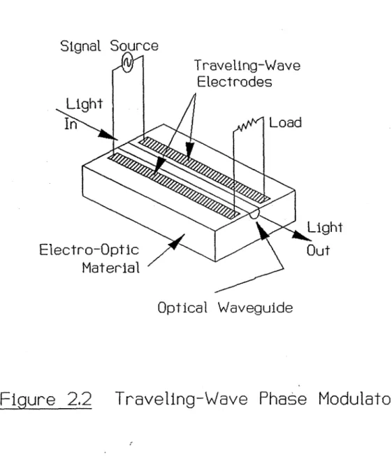
2.4 The Traveling-Wave Phase Modulator
If the electrodes are viewed as a transmission-line with distributed inductance as well as distributed capacitance, they can be designed to have the same
impedance as the signal source (assuming a real signal-source impedance -
usually 50R). The electrodes are driven at one end by the signal source, and
are terminated at the other end by a matched load (Figure 2.2). Now the
signal source is presented with a matched load at all frequencies, and there is no
R-C rolloff at high frequency. The penalty for this bandwidth increase is a loss of modulator sensitivity. The low-frequency response of the modulator is
halved because of the matched load, as compared to the capacitor-type
electrodes. In order to get the same phase-modulation as a capacitor-type
electrode at low frequency, the traveling-wave type must be driven by a signal-
generator capable of supplying 4 times as much power - i.e., the matched
termination costs 6 dB in responsivity.
Although the traveling-wave modulator does not suffer from the R-C bandwidth limitation, it does suffer from limitations of its own. These occur at a much
higher frequency, where the electrodes are no longer short compared to a
wavelength. As we have already noted, LiNbOQ has a much higher refractive
index for rnicrowave/millimeter waves than for optical signals, which means
that the microwave/millimeter wave modulating signal is propagating more
Optical Waveguide
and this imposes bandwidth limitations.
2.5 Frequency Response of the Traveling- Wave Phase Modulator
In expression (12) above, the phase deviation depends on the electric field strength E,. However, this expression was derived for a DC electric field, and the applied field is now an RF field. Solving the rather ugly nonlinear wave equation that results from having the two signals propagate in the lithium
niobate (which is dispersive between them) is not a practical idea. It is much
easier to find the "average electric field strength experienced by an optical
wavefront as it propagates through the modulator.'' To do this, assume that
the wave's velocity is not affected by the modulation (which is true to a very
good approximation).
Suppose that the effective refractive index experienced by the modulating signal
as it propagates along the electrode structure is n,. Then the modulation
signal propagates at c/n, while the optical signal propagates at c/nopt. The
time taken for each to travel a distance x is:
18
urn x
# =- c (am - "opt)
,
where w, is the modulating signal angular frequency (= 2 n f, ).
The largest mean value of the electric field "experienced7' by any optical wavefront is now given by the integral
urn
2 sin(? (n, L
- Em - "opt)
)
- L W In
7 (nrn - nopt)
Substituting this for E, in expression (12) gives the frequency response of a traveling-wave electro-optic phase modulator:
The response is a sinc-function in frequency (w,), but the interaction length L appears in front of the sinc-function as well, and so the response is sinusoidal in L. If the two signals propagate along the structure at the same velocity (n, =
LiNb03, the modulating signal experiences an effective refractive index intermediate between that of air (n=l) and that of LiNbOg (n=5.3). The refractive index experienced by the modulating signal is 3.8 (=
-
4
). The light propagates much faster than this in the optical waveguide, where nOpt2.6 The Mach- Zehnder Amplitude Modulator
Photodetectors are insensitive to phase modulation, but sensitive to amplitude modulation. In order to make use of the phase-modulators described above, one must convert the phase modulation to amplitude modulation. The most common way to do this is to use a Mach-Zehnder interferometer (MZI) - see Figure 2.3.
Optical
Waveguide
E l e c t r o d e s
i n
Ficrure
2,3
Mach-Zehnder Interferometer
Output
Intensity
o
Normalized Bias Voltage
single-mode. If it is multimode, then much of the light which should have
scattered into the substrate will be converted to other guided modes, and will
appear at the output of the modulator. This will reduce the amplitude
modulation of the output signal appreciably.
It is possible to drive the phase modulators with electrical signals of different
amplitudes. The extreme example of this is to drive only one of the phase
m~dula~tors, in an unbalanced MZI. This produces combined amplitude and
phase modulation, which may be viewed as an amplitude modulator with
frequency-chirp. This is not desirable in most cases; one of the potential
advantages of external modulators is that they can be chirp-free. However, if
the unbalance is small, the chirp is also small, and Korotky et al. [2] have claimed some advantages for communications if the chirp is tailored to the fiber
characteristics.
The modulator converts phase modulation to amplitude modulation most
linearly when driven with a small signal, with a "bias"-phase difference of 90".
Because of the symmetry about this operating point, there is no second-
harmonic generation due to the sinusoidal nonlinearity, but there is third-
harmonic generation. For good linearity, the phase-deviation about the bias-
point must always be kept small. On the other hand, for digital operation the
phase-difference must be zero or 180" to turn the modulator full on or full off.
While one might expect that a symmetrically-constructed modulator would
have zero phase-difference between the two paths, it is not usually possible to
strongly pyroelectric and piezoelectric, so that small temperature gradients or
strains in the crystal will produce electric fields which will alter the optical
phases in the two paths via the electro-optic effect. A LiNbOQ modulator must be biased to its operating point, and the bias will need to have active control to
maintain the desired 90° operating point, which will otherwise wander slowly.
One way to do this, for example, is to monitor a pilot-tone, and adjust the bias
until the second-harmonic of the tone is zero at the output. There is an
additional bias problem, as there is a tendency for LiNbOQ modulators to show
some bias-drift even when the temperature and physical conditions are carefully
controlled. This may be due to surface effects, and is being studied 131.
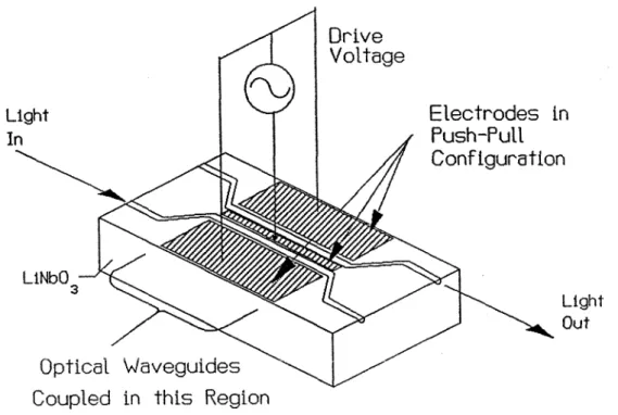
2.7 The Ap Coupler Modulator
The A,6' modulator (Figure 2.5) operates on an entirely different principle from
the phase-modulator-based Mach-Zehnder. It is an amplitude modulator which
depends on coupled-mode theory. Small variations in the propagation velocities
in two coupled optical waveguides can produce large variations in the amount of
power coupled from one waveguide to the other. In the next few sections I will
discuss the theory behind these modulators. Much of what I will present is discussed by Yariv [4], but I have collected and re-ordered the material found there and have changed the form of the results for the purpose of interpretation.
2.8 Theory of Coupled Modes
In this section I will present a formalism for describing coupling between modes.
Electrodes
in
Optical Waveguides
Coupled i n t h i s Region
The medium polarization P(r,t) can be written as
where Po(r,t) = [ ~ ( f ) - €0
1
E(r1t) (23)is the polarization of an unperturbed waveguide whose dielectric constant is ~ ( r )
.
The perturbation introduces coupling between modes. When we substitute (22) and (23) into (21) and write out only the y-component we obtainSince we are dealing with a system which supports only confined modes, we can write the y-component of the mth such mode as gy(m)l where
and we can write Ey as a superposition of such modes:
Ey(r,t) =
a
Am(z) kJrn)(x) e'(wt - U 1 n z )+
constant. (26) mNote that z is the direction of propagation and x is the transverse direction orthogonal to y.
"slow" variation so that
we obtain
d Am
C
-jam7
g i m ) e'(Yt-'mt)+
const. = p - d 2 [ Ppert(r,t)ly
.
rn at2
(28) Now note that the modes 6y(m) are orthogonal, which means that
Using this fact, we take the product of (28) with by(')(x) and integrate from
- co to oo, which gives the result
A,(-) is the coefficient of the wave traveling in the -z direction, and A,(+) is the coefficient of the wave traveling in the +z direction.
2.9 Directional Coupling
We now have the framework of coupled-mode theory available so that we can
refractive index distributions are given by n,(x) and nb(x). The transverse field distributions for each waveguide alone are gy('")(x) and gyO)(x), with propagation constants
Pa
andPb.
Let the complete coupled structure have index distribution n,(x), with propagation along the direction z. We can now approximate the field in the coupled structure as the weighted sum of the fields which would exist in either structure alone.If the two waveguides are not coupled then A(z)=A(O) and B(z)=B(O) for all z. If the waveguides are coupled, then A and B will vary with z. Substituting (31) into (22) and (23), we have
Now we can apply the result at the end of the section on coupled-mode theory, by substituting for Ppert in (30). This produces two coupled differential equations, which are:
The terms M a and M b represent a small correction to the propagation constants
pa
andPb
due t o the presence of the second guide. If we now rewrite the totalfield as
where
instead of the earlier approximation (31), and assume symmetry between the guides, we get a slightly different set of coupled differential equations (c.f.(33)):
dA - - j B e-.7.26t
--
dz
j2Sz * = - j K A e dz
where 2" &, 1 -
Pal
1Note that conservation of energy requires that
The solution of (38) subject to boundary conditions B (O)=B,, A(O)=O, is
B (z) = B, ej6"
{
c o s ( \ ] m z) - j s s i n ( \ i ' 2 " T 2 ~ ) } . ( 4 1 )\]k2+sZ
I now define Al(z) and Bl(z) according to:
Now, using (42) and (39) in (36) we find that:
- ( P a , l + @ b , l Coefficient of gy(")(x) ejwt = Al(z) e 2
1
Z ,- j ( P a , l + P b , l
Coefficient of gy(')(x) ejwt = B ~ ( z ) e 2 ) z . (43)
Pa, 1 Pb, 1
In fact, these are the output fields if the input fields are
In terms of optical power, Po = Bo Bo*, and so the powers at the two output ports are given by:
2.10 The A/3 Coupler Modulator Analysis in Practice
These results are the theory behind a A@ coupler modulator. In a practical
modulator the material used to fabricate the optical waveguides is an electro-
optic material such as LiNbOj. When an electric field is applied to the
so we can substitute this in (46) to obtain
We now note that the power at port a depends on two dimensionless quantities, i.e., K Z and S / K . In fact, K Z is an angle, so we can define
We also note that the electric field strength is related to the voltage applied to the electrodes of the device by an effective distance d, so that V = dE. Then
Define V, according to:
The significance of scaling V, in the way I have indicated is that the value of 6
is usually chosen to be 7r/2 (or sometimes an integer multiple of 7r/2). In the case where 6 = 7r/2, then P,=l when V=O, and P,=O when V=V,. In other words, V, is the switching voltage of a modulator where ~L=7r/2. Note that V, does not itself depend on the length of the modulator, only on its cross-section.
The transfer-function of this modulator, as given in (52) and Figure 2.6, is not linear, of course. The modulator is usually operated at the point of inflection of the transfer function so that there are no second-order products. However, third and higher-order products will be present, giving rise to significant distortion which may be unacceptable in some analog applications. The distortion performance of this modulator is very similar to that of the Mach- Zehnder modulator, as pointed out by Halemane and Korotky 151, and the same bias-point stabilization considerations apply.
Output
Intensity
o
Normalized Bias Voltage
2Figure
2.6
Transfer Function of
the entire length of the modulator. Unfortunately this is not possible in the
case of a directional coupler. This is because the coupler is a four-port device.
The coupler is characterized by a transfer matrix of the form
where al and bl are the field strengths at the two output ports, a, and b, are
the field strengths at the input ports, and A and B are similar to S-parameters. The analogous process would be to divide the modulator into an infinite
sequence of infinitesimally short lengths of coupler, each with the appropriate
value of 6, and take the product of their transfer matrices - where the number
of these matrices is infinite. This is not done. Korotky and Alferness 161
computed the time-domain impulse response of the rnodulator and took the
Fourier transform of this. However, as Chung and Chang
[?I
point out, the modulator is nonlinear, so this is not a true small-signal frequency response.They obtained a perturbation solution by expanding a matrix differential
equation - similar to (33) - as a power series and taking only the first term,
producing a linear matrix differential equation which could be solved. Their
where AI(w) is the small-signal change in intensity as a function of frequency for a given drive level, and
The normalized frequency response is then given by
According to this theory, for a LiNb03 modulator where there is no attenuation of the modulating signal ( a = 0), and where the effective microwave refractive index is 3.8, the bandwidth of a Mach-Zehnder interferometer modulator is given by
So, in fact, the directional coupler has some 28% greater bandwidth.
Remember, however, that this assumes no attenuation of the modulating signal
in the electrodes, which is an unrealistic assumption. For a complete model of
the frequency response, a model of the attenuation, including its frequency-
dependence, would be required.
References
[I] M. Izutsu, Y. Yamane, and T. Sueta, "Broad-Band Traveling-Wave
Modulator Using a LiNbOQ Optical Waveguide," IEEE J. Quantum Elec., Vol.
QE-13, No.4, pp. 287-290, April 1977
[2] S. Korotky, remarks made at Engineering Foundation Conference on High- Speed/High-Frequency Optoelectronics, held at Palm Coast, Florida, March 17-
22, 1991 (no proceedings published)
[3] R.L. Jungerman, et al., "High-Speed Optical Modulator for Application in Instrumentation," J. Lightwave Tech., Vol. 8, No. 9, pp. 1363-1370, September
1990
[5] T.R. Haleniane and S.K. Korotky, "Distortion Characteristics of Optical Directional Coupler Modulators," IEEE Trans. Microwave Theory &
Techniques, Vol. 38, No. 5, pp. 669 - 673, May 1990
[6] S.K. Korotky and R.C. Alferness, "Time- and Frequency-Domain Response
of Directional- Coupler Traveling- Wave Optical Modulators," IEEE J.
Lightwave Tech., Vol. 1, No. 1, pp. 244-251, March 1983
3. The Antenna-Coupled Modulator Concept
The analysis in Chapter 2 showed that the phase-velocity mismatch between
the light and the modulating signal resulted in a sinc-function frequency
response. The length of the modulator electrodes determined the cutoff
frequency and the DC sensitivity, resulting in a constant sensitivity-bandwidth
product. This means that if the modulator is to work a t a high frequency it
will have to be short and its sensitivity will be low, i.e., it will take a large
driving voltage t o produce a given phase-deviation.
It is possible to get a larger phase-deviation by positioning several sets of
electrodes along the optical waveguide. The phase-velocity mismatch in each
electrode segment produces some phase-error over its length, but with
appropriate design the phase-error can be corrected at the start of the next
electrode segment. This can be done in a number of ways [I-31. Perhaps the
best-known is the phase-reversal modulator (Figure 3.1). In this design the
electrode segment length is such that the phase-error at the end is 90". At this
point the electrode structure reverses the electric field polarity, giving a -180°
phase-change, so that the phase-error is now -90". This procedure can be
repeated any number of times, inserting a phase-reversal every time the phase
error reaches 90". There are also aperiodic phase-reversal designs [Z]. An alternative approach, taken by Schaffner [3], uses a filter-type structure with
delay stubs to produce the correct phase-veloci ty along the structure (Figure
3.2).
Signal
frequency, but are essentially fil ter-struct ures. As more electrode segments are
added the sensitivity of the modulator at the center frequency increases, but the
bandwidth decreases (Figure 3.3). Also, in practice it is not useful to keep adding more segments, because the modulating signal is attenuated at each
step, so that eventually any additional electrode segments have little effect.
Bridges and Schaffner have suggested another idea, again involving a number of
short modulator segments. They have proposed that the modulating signal be
split into several parallel paths - actually delay-lines - whose lengths are chosen
so that the signal arrives at the input to each modulator segment a t exactly the
right time to achieve proper phasing of the modulator segments. This method
would achieve the rephasing by true time-delay, which has the advantage of
working equally well at all frequencies - i.e., this is not a filter. A patent is
pending on this idea.
The antenna-coupled modulator concept, originally proposed by Bridges (U. S. Patent No. 5, 076, 655), also achieves rephasing by true time-delay, so that it
has no center-frequency and the bandwidth is independent of the number of
segments. Each electrode segment is connected to its own surface antenna
(Figure 3.4). The antennas are illuminated by the modulating signal at the
angle which delays the modulating signal by the correct amount from antenna
to antenna. This differs from the other approaches in a number of ways.
Since the phase is corrected by a true time-delay method, rather than a filter
structure, the bandwidth does not depend on the number of segments, but is
Figure
3.3
Frequency Response of
F i o z
3.q
w-J
---
The modulating signal drives the antennas in parallel, not in series, with the power divided equally between the antenna/electrode segments.
Consequently the nth segment is driven with the same power as the lSt or any other segment - attenuation in the electrodes does not limit the number of segments which can be used.
Millimeter-wave signals often originate in waveguide systems, which are compatible with the radiative feed required for this approach. Coax-to- electrode connections, with their associated parasitics, are not necessary
Although "manufacturing defects" are not usually considered, we note that a short-circuit in one antennalelectrode segment only degrades the performance by a small amount, while a similar defect in any other modulator renders the whole modulator entirely useless.
However, there are a few ways in which this approach is less attractive.
.
The bandwidth of the modula,tor is determined by the bandwidth of the antennalelectrode elements. Antennas never have a DC response, and simple antennas have small bandwidths. Nevertheless, the bandwidth will be greater than for phase-reversal or other filter-type modulators, and useful bandwidths are feasible.from electrode to electrode) increases as the number of electrode elements n, the sensitivity of the antenna-coupled modulator increases as m.
As the number of antenna/electrode elements becomes large, the incident
modulation signal must be kept very close to a plane wave. This amounts to
a tradeoff between sensitivity and spatial bandwidth (in the sense that the
incident signal may be represented as a spectrum of plane-waves, and this
spectrum must be very limited).
The dimensions of the modulation-signal feed can be quite large, especially
when the number of antennalelectrode elements becomes large, requiring the
feed to radiate the signal to the antennas with very small spatial bandwidth.
There remains the problem of finding the correct feed anglc for the modulating
signal. To understand how this works, consider Figure 3.5. If a signal is
incident on the antenna array from the end, then its phase-velocity along the
array is c/n, where n is the refractive index of the medium. If the signal is
incident on the array from the side ("broadside"), then all the antennas are
driven in the same phase, and the phase-velocity of the signal along the array is
infinite. Thus any phase-velocity greater than c/n is possible by choosing the
correct angle of incidence. In this case, the phase-velocity to match is the
phase-velocity of light in the optical waveguide, i.e.,
.
This is less than c, so the method will not work if the modulating signal is propagating in free space.However, the index of LiNb03 is about 5.5 for the modulating signal, so the
method will work if the modulating signal is incident on the antenna array from
Positions o f Antennas
Velocity
-I; k
Set 9 so that
c - C
nm sine - nopt
Flqure 3,s Angle-Matching o f Phase Veloclty The antennas are located at the interface
between LiNbO and air, The positions of the
3
antennas are shown In the diagram, , The modulating
signal is incident on the antenna array from
inside the LiNb03 at the angle which provides a
are much more responsive to signals incident from inside the dielectric than to
signals incident from the free-space side. The correct angle of incidence, 8, is at
about 23" to normal ("broadside") incidence.
References
[I] R.C. Alferness, S.K. Korotky, and E.A. Marcatili, "Velocity-matching techniques for integrated optic traveling-wave switch/modulators," IEEE J .
Quantum Electron., Vol. QE-20, pp. 301-309, 1984
[2] N. Zhu and Z. Wu, "Optimization of phase-reversal traveling-wave optical modulators," Microwave and Optical Tech. Lett., Vo1.2, No.?', pp. 240-244, July
1989
[3] J.H. Schaffner, "Analysis of a millimeter-wave integrated electro-optic
4. Antenna-Coupled Modulators - Theoretical Considerations
4.1 Antennas on a Dielectric Half-Space
Since the electrodes of the antenna-coupled modulator are on the surface of the ILiNbO3 electro-optic material, the antennas will be on the interface between LiNb03 and air. The behavior of antennas is changed fundamentally by the presence of a dielectric interface like this. The simplest way to look at this effect is to assume that the LiNbOj is infinitely thick and examine the behavior of antennas on a dielectric half-space. A number of papers have been written on various aspects of this [l - 51. I will not go into a detailed examination of the physics involved here, but in Appendix A I derive antenna patterns for wire antennas on a dielectric half-space based on physical insight into the mechanism by which the antenna pattern is determined.
the interface and the antenna response is large.
Examples of the antenna-patterns of interfacial antennas are illustrated in
Figures 4.1 - 4.3. Figure 4.1 shows the H-plane pattern of a dipole on a half-
space of dielectric constant ~ = 4 . (The antenna is normal to the plane of the
diagram.) Note that there is very little coupling to the air-side of the interface.
Almost all of the power is radiated into the dielectric. A notable feature of the
antenna pattern is the cusp in the pattern on the dielectric side. This cusp
occurs at the critical angle, i.e., at 30° in this case. Figure 4.2 is again a H-
plane pattern of a dipole, but this time on a high-dielectric material, ~ = 3 6 .
This time there is virtually no coupling at all to the air-side of the interface.
The cusp occurs at 9.6O now. If the length of the antenna is increased, and it is
bent to form a V-antenna, quite different antenna patterns are possible. Figure
4.3 shows the H-plane pattern of a V-antenna on a dielectric half-space of c=28.
In this case the length of each arm of the V is one wavelength from end-to-end
at the interface, where the effective refractive index is
-
4
= 3.8. The V angle is 100". This figure is taken from Appendix A, which goes into detailon the subject of wire antennas on dielectric half-spaces.
The fact that the antenna couples more efficiently into the dielectric is a
fortuitous one. As we saw in Chapter 3, the modulating signal must be incident
on the antenna array from inside the dielectric in order to achieve the necessary
phase-velocity-match condition. This fits in nicely with the antenna's
Figure
4.1
H-Plane Pattern of a Straight Dipole
Figure 4.3
Antenna pattern of a V antenna on the surface of adielectric, c-28, Each arm of the V i s one surface-wavelength long. The V angle i s 1 0 0 ~ . The pattern shown i s in the
4.2 Modulation Efficiency as a Function of the Number of Antennas
The idea behind the antenna-coupled modulator concept is to allow the
interaction length of the modulator to be made large so that the modulation
efficiency (the total phase-shift per arm for a given input modulation signal
power) can be increased. However, if there are two antennas then the power is
split between them, so although the interaction length increases, the drive-
power per unit length decreases. How does the net modulation efficiency
behave?
The phase-shift depends on the modulating signal field strength and on the
interaction length. The modulating signal power is proportional to the square
of the field strength, which is to say that the field strength is proportional to
the square root of the modulating signal power. When the number of
antenna/electrode segments is increased from 1 to N, the total interaction length increases from L to NL, while the signal power per element decreases from P to P/N. This causes the field strength to decrease from E to E/
4 T .
The net change in modulation efficiency is then from qLE to T ~ ( N L ) ( E / ~ ) =
. \ ~ N ~ L E (where q is the constant of proportionality which relates modulation efficiency to Length x Electric Field). So an N-element antenna-coupled modulator will be more efficient than a single-element modulator by
m.
It is instructive to compare this with a phase-reversal-type modulator. If there
is no attenuation of the modulating signal, the electric field strength is
independent of the number of phase-reversal sections because they are
signal, so beyond some value of N there is very little further benefit to increasing the number of sections. Second, as I've noted previously, phase- reversal modulators are filters, and the bandwidth of the modulator decreases rapidly as N increases. The bandwidth of an antenna-coupled modulator is independent of N. The tradeoffs involved in choosing to drive modulator elements in series or parallel, and other power-split optimization considerations, are addressed in Appendix B.
4.3 Modulator Beamwidth and Phasefront Curvature
increasing the interaction length (as there was in the case of the phase-reversal modulator) there is a spatial bandwidth penalty. The modulation signal must be radiated onto the antenna array with greater angular precision, and its phasefronts must be increasingly flat. Figure 4.4 shows an example of a rnodulator antenna pattern for a modulator with 18 antennalelectrode segments and an overall length of 3.6 A,, and Figure 4.5 shows how the modulation sensitivity of this rnodulator varies with phasefront curvature.
4.4 Feed Design
The importance of illuminating the antennas with the modulation signal in the correct way has been discussed above. The problem of doing this is the problem of feed design. Usually we would expect the mm-wave modulation signal to be corning from a rectangular metal waveguide. The feed should convert this guided wave so that it arrives at the antenna array with flat phasefronts at the correct angle of incidence. In addition, it should do so efficiently, losing as little power as possible to radiation, impedance mismatches, or overspill past the antenna array.
Main
L
F i ~ u r e
4,4
Antenna Pattern
o f
a Modulator
w i t h
18
Dipole
Antennas on
E
=36.
Normalized
Response
(
Deg/J(;S-
110
Radius
of
Curvature 10000F i g u r e
4.5
Modulator Response as
a
Function o f Phasefront Curvature,
This
i s
the Modulator whose
Antenna Pattern
is
shown i n
length of the antenna array. This is not quite sufficient, however. The
dielectric constant of the LiNbOQ is very high, and it is difficult to couple power
directly into a dielectric waveguide with high dielectric constant. It is easier to
couple the power into a lower dielectric constant material, then couple from this
low-dielectric-constant waveguide to a LiNbOQ waveguide. This requires a
matching network of some kind. The design of the feeds used in our
experiments will be shown in the chapter on the experimental results, but is
based on this concept.
References
[I] M. Kominami, D.M. Pozar, and D.H. Schaubert, "Dipole and Slot Elements
and Arrays on Semi-Infinite Substrates," IEEE Trans. Ant. & Prop., Vol. AP-
33, No. 6, pp. 600-607, June 1985
[2] N. Engheta and C.H. Papas, "Radiation Patterns of Interfacial Dipole Antennas," Radio Science, Vol. 17, pp. 1557-1566, November-December 1982
[3] G.S. Smith, "Directive Properties of Antennas for Transmission into a Material Half-Space," IEEE Trans. Ant. & Prop., Vol. AP-32, No. 3, pp. 232-
246, March 1984
[4] R.C. Compton, R.C. McPhedran, 2. Popovic, G.M. Rebeiz, P.P. Tong, and
D.B. Rutledge, "Bow-Tie Antennas on a Dielectric Half-Space: Theory and
Experiment," IEEE J. Ant. & Prop., Vol 35, No.6, pp. 622- 631, June 1987
Antennas," Chapter 1, Infrared and Millimeter Waves, Vol. 10, Academic Press
5. Antenna-Cou~led Phase Modulator a t 10 GHz
5.1 Design of the Prototype Modulator
In order to demonstrate the antenna-coupled modulator concept, we decided to build a prototype modulator at X-band. This prototype modulator should be as simple as possible, so that we would be able to understand its behavior. We chose to leave the modulator electrodes unterminated because of the practical difficulty of fabricating matched terminations for the electrodes at X-band, and because this problem would be even greater at mm-wave frequencies. We also decided to use simple dipole antennas, because we had a theoretical model for dipoles on a dielectric half-space. We chose to design a phase modulator rather than an intensity modulator. This is simpler to fabricate because it has no Y-
junction in the optical waveguide (it consists of a single optical waveguide going from one end of the LiNb03 substrate to the other) and because it requires no DC bias to operate correctly (intensity modulators must be operated at the proper bias-point). Finally, we designed the optical waveguide for light at the HeNe wavelength of 0.633 prn, because experiments are easier when the beam is visible, and because HeNe lasers produce a nice, narrow, single-mode output, and because we happened to have some HeNe lasers available.
Figure
5.1
The
18
GHz
Prototype Modulator
lengths were optimized using the theoretical model of the modulator. We had intended to optimize the modulator for 10 GHz, but it turned out that we were using a slightly wrong effective refractive index value in the model (4.6 instead of 3.8). When the correct index is used, the design turns out to be optimized nearer to 12 GHz.
5.2 Theoretical Model of the Modulator
The idea behind keeping the prototype modulator simple was to allow us to model it and show that its behavior could be accounted for. Thus, we needed to develop a theoretical model of the modulator. We were interested in the modulator's frequency response, its absolute sensitivity, and its spatial frequency-response (i.e., its sensitivity to being illuminated by the RF at the wrong angle of incidence).
We begin by looking at the transmission line electrode and the interaction between the modulating signal on the transmission line and the optical signal in the waveguide beneath. For a conventional traveling-wave modulator the modulation coefficient
6
is a function of the transmission line lengthL,
the optical refractive index n, the effective transmission line index n,, and the modulation frequency f,(=
*
)
.
The relationship between these can be27r written:
6
a L Sinc(9
(n -antenna. If the antenna is not well-matched to the transmission line there will
be multiple reflections. Nevertheless, the various waves on the line may be
summed to give one resultant wave propagating down the line to reflect (once)
at the end. Then
6
u L [ S i n c { E ( n - n,) L } + Sinc{%(n 2 c +n,)L}]
.
(2)Equation (2) allows us to compute the frequency-response of the electro-optic
interaction, as determined by the phase-velocity mismatch.
Next I want to consider the amplitude of the modulating signal propagating on
the transmission line. The bigger the modulating signal voltage, the more
modulation we can expect. If the transmission line is low-loss (which it is, over
the short length of the line) then the forward-propagating part of the
modulating signal and the backward-propagating part (reflected) have the same
amplitude and are in phase at the open-circuit end of the line. The amplitude
of the forward-propagating wave is therefore half the amplitude of the signal at
the open-circuit. Referring to Figure 5.2, the analysis is very simple.
Antenna Transmission Line Electrode
Figure
5.2
E q u i v a l e n t
C i r c u i t
Model
Hence
I
'fwdI
=I
Va 2I
z
o1
Za Sin 0 - j Zo Cos 0I
'
where Pa is the power the antenna could deliver to a matched load Z=Za*
Hence
1
V f ~ d1
= 20d-'TJ%-
\I
~ , 2
sin2@+
( Xa Sin 0 - Zo Cos B )2Equation (10) allows us to calculate the frequency response of the modulator if we know the center-frequency electrical length 0 of the transmission line, its impedance Z,, and the available power Pa and impedance Za of the antenna (which itself may be a function of frequency).
where
r = a + j p .
(12)Kominami et al. [I] have calculated antenna impedances for dipoles on a variety of substrates, although unfortunately they did not consider LiNbOj. However, extrapolation of their results would suggest that for a dipole on a substrate of e-36 the antenna impedance is close to
where 6 (= 0.5 /3 La) is the electrical half-length of the antenna.
The power the antenna can deliver to a matched load, Pa, is a function of frequency also. Over narrow frequency ranges it can be assumed to be constant, but over wide frequency ranges it cannot. I made a very rough approximation to Pa by plotting the H-plane pattern of the dipole antenna (see Appendix A) and estimating the change in gain (and thus Pa) with frequency from the change in beamwidth. This resulted in the equation:
The transmission line itself is coplanar strip line. Rutledge et al. [2] have given
the characteristic impedance (and also radiation loss) of this transmission line.
Suppose the total width of the electrodes is W, and the gap between them is s,
as in Figure 5.3. Then
K(k)
20 = rlm- K'(k) (15)
and "'ad = I q k ) 20.2 K(k) ( 1 dB/Xd,
'
d (16)where
and
and
and
For the prototype modulator we used W=100 pm, s=8 pm, giving 2, E 35 0.
We constructed a model of the modulator based on this information about the
components. This model was to provide frequency response information only,
not absolute response information. The predicted frequency response is shown
Electrodes
A X
C r y s t a l
I
Axes
I
4 5 6 7 8 9 10 1 l . u 1s
Frequency (GHz)
5.3 Fabry-Perot Measurement Technique
Since the prototype modulator was a phase modulator, it was not possible to measure its performance by monitoring the output of a photodiode illuminated by the modulated optical beam. Photodiodes are completely insensitive to phase modulation. Instead we used a scanning Fabry-Perot interferometer as an optical spectrum analyses to look for the modulation sidebands. The Fabry- Perot is a very narrowband optical filter (bandwidth=13 MHz in the case of our Spectra-Physics 470-03), and by scanning its passband it is possible to measure only the light in the carrier at the photodiode, stripping off the power in the modulation sidebands, or conversely to measure the power in either of the sidebands alone.
When a carrier at frequency f, is phase-modulated by a signal at modulation frequency f,, it produces an infinity of sidebands at f,
f
nf,, n=1,2,3....
For small-signal modulation, however, only the two sidebands at fc+ f, and f, - f, are significant. In this case each of these sidebands has sideband power5.4 Experiment a1 Setup
The modulator fabrication process is outlined in Appendix C, so I will not go into those details here. The experimental setup is shown in Figure 5.5. The
optical signal source is a HeNe laser (Aopt= 0.633 prn), mounted on a Z-axis translation stage for positioning. The optical beam (Gaussian, with diameter =
3 mm) is coupled into the modulator by a 40x microscope objective which
brings the beam down to a beamwaist (diameter = 2 pm) at the optical waveguide input. At the output of the optical waveguide (at the other end of
the modulator) there is another 40x objective which collimates the optical
output into an output beam. This beam enters a scanning Fabry-Perot
interferometer which is used as an optical spectrum analyser, as discussed
above. The modulator itself is mounted on the face of a dielectric wedge, through which the modulating signal propagates. The dielectric constant of the
wedge material (stycastR artificial dielectric from Emerson & Cuming) is 30 to
approximate that of LiNb03, and the wedge is cut so that the modulating
signal is incident on the antenna array at the required 23" angle. The
modulating signal is coupled into this wedge from a rectangular metal
waveguide via two quarter-wave matching layers of c=3 and c=10, again using
Emerson & Curning dielectric material (these values of t: do not provide precise
matching, but the resulting match is effective over a wider bandwidth). The
modulating signal source for the experiment was a Hewlett-Packard 0.01-20
GHz sweep oscillator. Because the experiment covers such a wide frequency
range (5 - 13 GHz) it was necessary to use two different sizes of metal waveguide in the modulating signal feed (WR-137 & WR-90). Interestingly,
there seems to be no change in the response of the modulator at the point where
Laser
on
2-Axis
Stage Microscope O 5 e ctives oo 3 - A x i s Stages
same.
As this experiment involved aligning the optical elements, I will describe, briefly, how this was done.
Once the laser, microscope objectives, modulator and Fabry-Perot had been positioned approximately, the first step was to set the focus of the input microscope objective lens at the end-face of the modulator substrate. When the light, entering through the lens, struck this endface, some of it reflected back through the lens toward the laser. I put a beamsplitter in the path between the laser and the lens so that I could direct this reflected light onto a white card (since the wavelength was 0.633 pm I could see the beam on the card). When the lens was focussed properly the reflected beam was re-collimated by the lens and this produced a sharp spot on the white card.
Next the output lens position was adjusted so that this lens was positioned as far from the output