883 | P a g e
VERIFICATION AND SIMULATION OF NEW
DESIGNED NAND FLASH MEMORY CONTROLLER
M. Santhi Kumar
Asst. prof in ECE, Newton’s Institute of Engineering, Macherla
ABSTRACT
In this paper a NAND flash memory controller was designed. For the best use of NAND type flash memory we design a new Arithmetical and Logical Unit (ALU) for calculating increment, addition, subtraction, decrement operations etc. In this memory controller we design single memory cell, memory module, a decoder etc. These all are encapsulated inside a controller and this is on top most in hierarchy. NAND flash memory is a non volatile storage media used in today daily life electronic equipments. NAND flash memory is programmed on page by page basis. Typically programming time is very less few micro second per page. This NAND flash memory controller architecture can be used with a real secure digital card, multimedia card (SD/MMC), digital cameras etc. The NAND Flash memory controller can be an internal device, built into the application processor or host, or designs can incorporate an external, stand-alone chip. Experimental results show that the designed controller give good performance and full fill all the system specifications. We have used FPGA chip for download our code.
Keywords-Flash memory; Non Volatile; Arithmetical and Logical Unit (ALU); Encapsulation;
Field Programmable Gate Array (FPGA); Secure Digital card/Multi Media Card (SD/MMC); Hard
Disk Drive (HDD)
I. INTRODUCTION
Flash memory is being widely used as a storage medium in mobile devices because of its low power
consumption, small form factor, and high resistance to shock and vibration. As the density of a flash memory
chip increases and the price continues to drop, the flash memory is being adopted in more diverse storage
applications. Flash memory is the combination of two technologies-EPROM and EEPROM. The term “Flash”
means - A large chunk of memory (memory cell) could be erased at one time”. On the other hand in EEPROM
each byte is erased one by one manner.
Flash memory has characteristics that are different from conventional storage devices such as HDD. Thus,
specialized hardware and software are required to use flash memory as a storage device. The role of flash
memory software is particularly important because it has to deal with the peculiarities of flash memory. It also
needs to be diverse because flash memory is used in a wide spectrum of applications ranging from
micro-embedded systems (e.g., a sensor-node) to large-scale servers [5]. Flash memory controller offers higher
capacity for fast data transfer and
884 | P a g e
hardware with NAND flash memory. NAND flash memory controller has also a bidirectional bus in betweenperipheral devices and controller, controller internal bus for various functional blocks and controller with
memory connections. For the improvement of product lifetime and system performance we always design an
excellent NAND flash memory controller. Single Level Cell (SLC) and Multi Level Cell (MLC) two techniques
are used for storing data in memory cells. SLC offers 100,000 erase program cycle while MLC offers about
10,000 erase programs cycle [2].
NAND flash memory controller has also a bidirectional bus (Data, Address, and Control). NAND flash cell are
placed together for saving 60% cell size over NOR flash cells. NAND flash memory controller provides a serial
access of data blocks in a very high speed [6]. Single Level Cell (SLC) and Multi Level Cell (MLC) two
techniques have been used for storing data in memory cells. Software called Flash Transaction layer (FTL) use
for wear leveling and bad block management technique. All vendors provide FTL software [9].
The pipelining and parallel processing concepts are applied for systematic design approach of a systolic array
processor. The systolic array architecture and iterative Very Large Scale Integration (VLSI) architecture is
applied for good performance. It makes the circuit design easy for implementation [8].
II. NAND FLASH MEMROY CONTROLLER ARCHITECHTURE
The capacity of NAND flash device is improved day by day, architecture are also improved day by day. Latest
overall structure of NAND flash device is looks very similar to its conventional structure. A NAND flash
controller implements memory mapped interface [10]. A multilane array packs contains its own set of
Cache/Data registers, more memory cells on a die and partitioned it into several plans. In multilane array packs
all operations performs parallels. Inside a single flash array operation time multiple pages of data can be
programmed, read, write, fetched etc. so average data access time is small. In multiplane commands some
addresses are restricted.
885 | P a g e
NAND flash controller has flash chips. In today life it is widely used in storage devices. One more recent application for flash memory is as a replacement for hard disks. Flash memory does not have the mechanical limitations and latencies of hard drives, so a Solid State Drive (SSD) is attractive when considering speed, noise, power consumption, and reliability. It always follows Open NAND Flash Interface (ONFI) standard [3]. In NAND flash device we have mainly I/O control block, control logic, NAND flash array. A NAND flash array includes two dimensional NAN D flash cells, Row/Column address decoder and cache / data registers [11]. It has a shared, multiplexed, bidirectional (command, address and data) I/O bus. Figure-1 shows the block diagram of a NAND Flash Memory Controller. A multilane array packs contains its own s of Cache/Data registers, more memory cells on a die partitioned into several plane. In multilane array packs, ll operations are performed in parallel. Thus, inside a single flash array, multiple pages of data can be programmed, read, write, fetched, so average data access time is reduced. In multilane commands some addresses are restricted. So new NAND flash chip with multitier and multilane support is always increase performance, reduce the data access average time, and increase parallel execution of commands [7]. NAND flash devices are programmed on a page by page basis. Typically programming time is a few hundred micro second per page. NAND flash cell can be programmed and erased only for limited time period (100, 00 0 times for SLC and 10,000 times for MLC) before it fails. To improve this limitation, flash memory performance has been increased by using wear leveling technique. The technique spreads the memory cell use evenly to different physical pages. So the entire flash device is used equally to improve the life of flash memory [2]. Bad block management technique and wear leveling technique use some remapping technique of logical to physical address of the memory device. They all provide an FPGA to facilitate the implementation of a wide range of NAND Flash Memory Controller [4].
III. SIMULATION AND RESULT
Single Micro cell Module
In the simulation result, the NAND flash memory cell is simulated using Xilinx ISE Software and modelsim simulator. As shows in Figure 2, the RTL view of NAND Flash memory cell has been gene rated after the synthesis. The modelsim waveform is displayed on Figure 3 indicating the write and read operation. Write operation takes place only when both word line and write enable are ‘1’. The q and qbar line are modified when this situation occurs as seen in the waveform and Read operation takes place when both word line and read enable should be high so that read out shows the data stored in q.
886 | P a g e
Figure 3. Simulation Waveform Single Micro Cell
IV. FULL ADDER
The simulation of full adder carried using Xilinx ISE Software and modelsim is shown in Figure 4. The RTL
view of full adder was generated after the synthesis and it displays the internal architecture of full adder. The
modelsim waveforms are displayed d in Figure 5 and depict the sum and carry output. Sum takes place only
when any one input is high and carry operation is done when at least two inputs are high.
Figure 4: RTL Schematic view of Full Adder
887 | P a g e
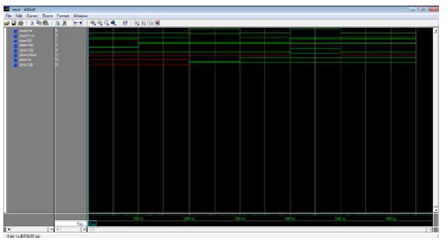
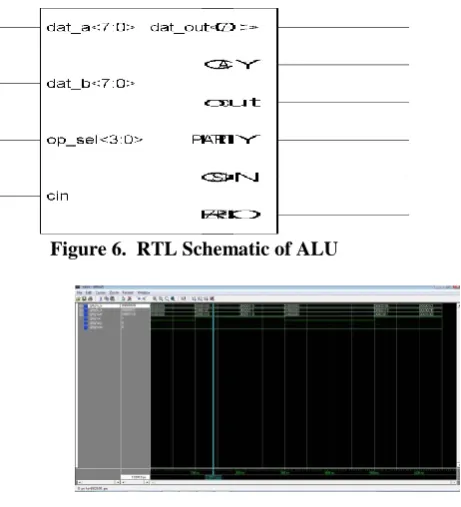
V. ARITHMETIC AND LOGICAL UNIT (ALU)
In the simulation, results of Arithmetic and Logical Unit (ALU) have been used in Xilinx ISE Software and
modelsim simulator as shown in Figure 6. The RTL view of ALU has been generated after the synthesis and it
displays the internal architecture of ALU. The mod else waveform is displayed in Figure 7 which indicates all
mathematical operations. The addition operation takes place only when Operation select lines are zero a nod
provide input value to the data and data band check the results on data out as well as all flag register like carry
flag, Sign flag, auxiliary carry flag, parity flag, etc. Thus all mathematical operation can be carried by changing
the value of sole.
Figure 6. RTL Schematic of ALU
Figure 7. Simulation Waveform of ALU
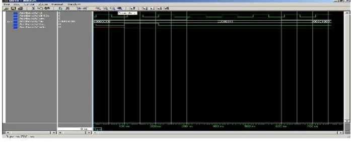
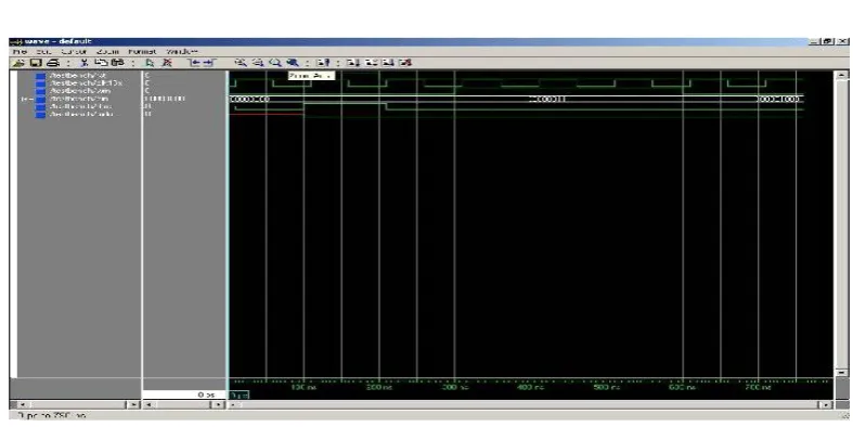
VI. MEMORY MODULE
In the simulation, result of Memory Unit using Xilinx ISE Software and modelsim simulator are shown in
Figure 8. The RTL view of memory unit is generated after the synthesis to display the internal architecture of
Memory Unit. The modelsim waveform is displayed in Figure 9. It indicates how the data can store in to the
memory with the help of read and write operation
888 | P a g e
Figure.9 Simulation Wave form of memory Module
VII. MEMORY READ CYCLE
In Figure 10, the RTL view of Memory Read Cycle has been generated after the synthesis to display the internal
architecture of Memory Read Cycle. The modelsim waveform is displayed in Figure 1 1. During Memory Read
Cycle when reset = „1‟ then both the mode operation are zero and when apply the clock pulse the data at ¼ and
¾points in data cell is generated and when increment the clock the data are in a position to g o from serial to
parallel conversion. After some time it will also shift to data register. In this way, data are shifted to the
particular data register and finally read the data at that location
Figure 10.RTL View of memory Read Cycle
889 | P a g e
VIII. MEMORY WRITE CYCLE
In Figure 12, the RTL view of Memory Write Cycle has been generated after the synthesis to display the
internal architecture of Memory Write Cycle. The modelsim waveform is displayed in Figure 13. During
Memory Write Cycle when reset = „1‟ then both the wrn1 and wrn2 operation is one and when enable the clock
detect the edge on write pulse. After some time, detect edge on write pulse to load transmit buffer. When
increment the clock the data are in a position to go from transmit shift register to transmit buffer. In this way,
data are shifted to the particular data register and finally write the data at that location.
Figure 12. RTL Schematic of Memory Write Cycle
Figure 13. Simulation waveform of Memory Write Cycle
IX. NAND FLASH MEMORY CONTROLLER
Figure 14 shows Xilinx RTL Schematic view of NAND Flash Memory Controller. Figure 15 are shows the
Simulation Waveform of NAND Flash Memory Controller. We bind all the above components inside this
module. This module is stand at the top of hierarchy. Various pins are described below-:
and_ale : This pin indicates NAND flash advanced latch enable when this pin is high, the NAND flash
memory controller work and when it is low, the NAND flash memory controller are in latch mode.
nand_ce: This pin indicates NAND flash chip enable. When this pin is high the NAND flash memory
controller are in working mode, it reflects that the data is storing in a memory in sequential order. When it
is low, the NAND Flash memory controller do not worked.
nand_cle: This pin indicates NAND flash clear mode. When this pin is high the data are cleared in the main
memory of NAND flash memory controller. When it is low it will not worked.
890 | P a g e
are in reset mode i.e. all operations of NAND flash memory controller stopped. When it is low, it willwork properly.
o nand_tri_en: This pin indicates NAND flash tri-state enable. When it is high, it will indicate the data are in tri-state i.e. high impedance state. When it is low it may work properly. between reset state (000), read ID
state (001), page state (010) and write page state (011). After that state 100,101,110,111 (4 states) reserve
for future extension
.
Figure 14. RTL Schematic of NAND Flash Memory Controller
Figure 15. Simulation Waveform of NAND Flash Memory Controller
X. CONCLUSION
In this paper NAND flash memory controller for SD/MMC memory card using FPGA was designed. The test
results show that NAND flash memory controller architecture will achieve a high performance. In the proposed
891 | P a g e
memory read cycle, memory write cycle have been developed. Proposed architecture can work with all theembedded computing system as a replacement of conventional Hard Disk Drive (HDD) with a very huge size of
NAND flash memory. In this controller we design only four states reset state, read ID State, read page state,
write page state. In future extension we have four reserve states.
XI. ACKNOWLEDGMENT
This work was supported by ShriRam Collage of Engineering and Management, Banmore
REFERENCES
[1] Shawn Kung, “Native PCIs SSD Controllers Next Generation Enterprise Architecture for Scalable I/O
Performance”, White Paper Marvell Jan-2012.
[2] Yang Ou, Nong Xiao, “A Scalable Multi-channel Parallel NAND Flash Memory Controller Architecture”,
6th Annual IEEE Chinagrid Conference, Page 48-53, 2011.
[3] Yu Cai, Haratsch, “FPGA Based Solid State Drive Prototyping Platform”, 19th IEEE Annual International
Symposium on Field-Programmable Custom Computing Machines (FCCM), Page 101-104, 2011.
[4] Yu Chi, Erich F. Haratsch, Mark McCatney and Ken Mai “FPGA-Based Solid State Drive Prototyping
Platform,” In IEEE International Symposium on Field Programmable Custom Computing Machines 2011.
[5] Yang Ou, Nong Xiao and Mingche Lai “A Scalable Multi-channel Parallel NAND Flash Memory
Controller Architecture,” Sixth Annual ChinaGrid Conference 2011.
[6]International Technology Roadmap for Semiconductor, 2007.
[7]Micron Technology, Boise, Idaho. Technical Note TN-29-17 “Design and Use Considerations for NAND
Flash Memory,” 2006.
[8]Altera Corporation, Stratix data isheet, May 2003.
[9] Intel Corp., Understanding the Flash Transfer Layer (FTL) Specification, 1998.
[10] Hoeseung Jung, Sanghyuk Jung, “Architecture Exploration of Flash Memory Storage Controller through
a Cycle Accurate Profiling”, IEEE Transactions on Customer Electronics, Volume: 57, Page 1756–1764,
2011.
[11] Teoh, J.N., Wong W.E., “FPGA Implementation of Nonlinear Control on Hard Disk Drive”, IEEE