c e-ISSN: 2348-6848, p- ISSN: 2348-795X Volume 3, Issue 01, January 2016
International Journal of Research (IJR)
Available at http://internationaljournalofresearch.orgDesign & Implementation of Area Delay Low Power
Adders in QCA Using VHDL Code
1
D. Mohammad
&
2K. Madan Mohan
1
M.Tech,VLSI, Dept of ECE, Intellectual Institute of Technology, Affiliated to JNTUA, AP, India
2Assistant Professor, Dept of ECE, Intellectual Institute of Technology, Affiliated to JNTUA, AP,
India.
Abstract
As transistors decrease in size more and more of them can be accommodated in a single die, thus increasing chip computational capabilities. However, transistors cannot get much smaller than their current size. The quantum-dot cellular automata (QCA) approach represents one of the possible solutions in overcoming this physical limit, even though the design of logic modules in QCA is not always straightforward. In this brief, we propose a new adder that outperforms all state-of-the art competitors and achieves the best area-delay tradeoff. The above advantages are obtained by using an overall area similar to the cheaper designs known in literature. The 64-bit version of the novel adder spans over 18.72 μm2 of active area and shows a delay of only nine clock cycles, that is just 36 clock phases. Parallel-prefix architectures, including Brent–Kung (BKA), Kogge–Stone, Ladner–Fischer, and Han–Carl-son adders, were analyzed and implemented in QCA in [13] and [14]. Recently, more efficient designs were proposed in [15] for the CLA and the BKA, and in [1] for the CLA and the CFA. In this brief, an innovative technique is presented to implement high-speed low-area adders in QCA.
Theoretical formulations demonstrated in [15] for CLA and parallel-prefix adders are here exploited for the realization of a novel 2-bit addition slice. The latter allows the carry to be propagated through two subsequent bit-positions with the delay of just one majority gate (MG). In addition, the clever top level architecture leads to very compact layouts, thus avoiding unnecessary clock phases due to long interconnections.
Keywords: Adders; noncompeting; quantum-dot cellular automata (QCA)
I. INTRODUCTION
Quantum-dot cellular automata (QCA) is an attractive emerging technology suitable for the development of ultradense low-power high-performance digital circuits [1].
For this reason, in the last few years, the design of efficient logic circuits in QCA has received a great deal of attention. Special efforts are directed to arithmetic circuits [2]–[16], with the main interest focused on the binary addition [11]– [16] that is the basic opera-tion of any digital system. Of course, the architectures commonly employed in traditional CMOS designs are considered a first reference for the new design environment. Ripple-carry (RCA), carry look-ahead (CLA), and conditional sum adders were presented in [11].
The carry-flow adder (CFA) shown in [12] was mainly an improved RCA in which detrimental wires effects were mitigated.
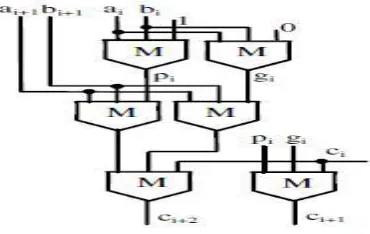
Fig. 1. Novel 2-bit basic module .
An adder designed as proposed runs in the RCA fashion, but it exhibits a computational delay lower than all state-of the- art competitors and achieves the lowest area-delay product (ADP).
The rest of this brief is organized as follows: a brief background of the QCA technology and existing adders designed in QCA is given in Section II, the novel adder design is then introduced in Section III, simulation and comparison results are presented in Section
c e-ISSN: 2348-6848, p- ISSN: 2348-795X Volume 3, Issue 01, January 2016
International Journal of Research (IJR)
Available at http://internationaljournalofresearch.orgII. BACKGROUND
A QCA is a nanostructure having as its basic cell a square four quantum dots structure charged with two free electrons able to tunnel through the dots within the cell [1].Because of Coulombic repulsion, the two electrons will always reside in opposite corners. The locations of the electrons in the cell (also named polarizations P) determine two possible stable states that can be associated to the binary states 1 and 0. Although adjacent cells interact through electrostatic forces and tend to align their polarizations, QCA cells do not have intrinsic data flow directionality.
To achieve controllable data directions, the cells within a QCA design are partitioned into the so-called clock zones that are progressively associated to four clock signals, each phase shifted by 90°. This clock scheme, named the zone clocking scheme, makes the QCA de-signs intrinsically pipelined, as each clock zone behaves like a D-latch [8]. QCA cells are used for both logic structures and interconnections that can exploit either the coplanar cross or the bridge technique [1], [2], [5], [17], [18].
The fundamental logic gates inherently available within the QCA technology are the inverter and the MG. Given three inputs a, b, and c, the MG performs the logic function reported in (1) provided that all input cells are associated to the same clock signal clkx (with x ranging from 0 to 3), whereas the remaining cells of the MG are associated to the clock signal clkx+1
M(abc) = a • b + a • c + b • c………. (1)
Several designs of adders in QCA exist in literature.The
RCA [11], [13] and the CFA [12] process n-bit
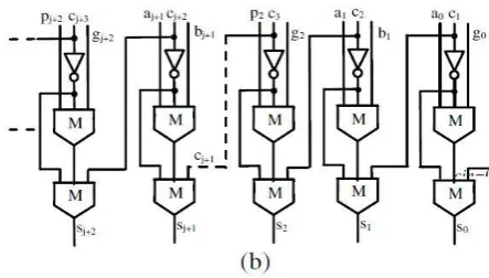
Fig. 2. Novel n-bit adder (a) carry chain and (b) sum block
Operands by cascading n full-adders (FAs). Even though these addition circuits use different topologies of the generic FA, they have a carry-in to carry-out path consisting of one MG, and a carry-in to sum bit path containing two MGs plus one inverter. As a consequence, the worst case computational paths of the n-bit RCA and the n-bit CFA consist of (n+2) MGs and one inverter. A CLA architecture formed by 4-bit slices was also presented in [11]. In particular, the auxiliary propagate and generate signals, namely pi = ai + bi and gi = ai • bi
,are computed for each bit of the operands and then they are grouped four by four. Such a designed n-bit
CLA has a computational path composed of 7+4×(log4 n) cascaded MGs and one inverter. This can be easily verified by observing that, given the propagate and generate signals (for which only one MG is required), to compute grouped propagate and grouped generate signals; four cascaded MGs are introduced in the com-putational path.
In addition, to compute the carry signals, one level of the CLA logic is required for each factor of four in the operands word-length. This means that, to process nbit addends, log4 n levels of CLA logic are required, each contributing to the computational path with four cas-caded MGs. Finally, the computation of sum bits intro-duces two further cascaded MGs and one inverter. The parallel-prefix BKA demonstrated in [13] exploits more efficient basic CLA logic structures. As its main advan-tage over the previously described adders, the BKAcan achieve lower computational delay. When n-bit oper-ands are processed, its worst case computational path consists of 4×log2 n−3 cascaded MGs and one inverter.
c e-ISSN: 2348-6848, p- ISSN: 2348-795X Volume 3, Issue 01, January 2016
International Journal of Research (IJR)
Available at http://internationaljournalofresearch.orgFrom the logic equations provided in [13], it can be eas-ily verified that the first stage of the tree introduces in the computational path just one MG; the last stage of the tree contributes with only one MG; whereas, the intermediate stages introduce in the critical path two cascaded MGs each. Finally, for the computation of the sum bits, further two cascaded MGs and one inverter are added.
III. NOVEL QCA ADDER To introduce the novel architec-ture proposed for implementing ripple adders in QCA, let consider two n-bit addends A = an−1, . . . , a0 and B = bn−1, . . . , b0 and suppose that for the i th bit posi-tion (with i = n − 1, . . . , 0) the auxiliary propagate and generate signals, namely pi = ai + bi andFPGA architec-ture logic block can be connected to the switch block. In the switch block there are four signals 1) data signal
(first bit) 2) data signal (second bit) 3) acknowledge-ment signal 4) data arrival signal. The above four signal acknowledgement signal and data arrival signal con-nected to pervious logic block.
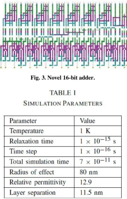
Fig. 3. Novel 16-bit adder. Fig. 4. Novel 32-bit adder.
With the main objective of trading off area and delay, the hybrid adder (HYBA) described in [14] combines a parallel prefix adder with the RCA. In the presence of n-bit operands, this architecture has a worst computa-tional path consisting of 2 × log2 n + 2 cascaded MGs and one inverter. When the methodology recently pro-posed in [15] was exploited, the worst case path of the CLA is reduced to 4 × _log4 n_ + 2 × _log4 n_ − 1 MGs and one inverter. The above-mentioned approach can be applied also to design the BKA. In this case the over-all area is reduced with respect to [13], but maintaining the same computational path. By applying the decom-position method demonstrated in [16], the computa-tional paths of the CLA and the CFA are reduced to 7 + 2 × log2(n/8) MGs and one inverter and to (n/2) + 3 MGs and one inverter, respectively.
Fig. 5. Novel 64-bit adder.
gi = ai • bi , are computed. ci being the carry produced at the generic (i−1)th bit position, the carry signal ci+2, furnished at the (i+1)th bit position, can be computed using the conventional CLA logic reported in (2). T
he latter can be rewritten as given in (3), by exploiting Theorems 1 and 2 demonstrated in [15]. In this way, the RCA action, needed to propagate the carry ci through the two subsequent bit positions, requires only one MG. Conversely, conventional circuits operating in the RCA fashion, namely the RCA and the CFA, require two cascaded MGs to perform the same operation.
In other words, an RCA adder designed as proposed has a worst case path almost halved with respect to the conventional RCA and CFA. Equation (3) is exploit-ed in the design of the novel 2-bit module shown in Fig. 1 that also shows the computation of the carry ci+1 = M(pi gici ). The proposed n-bit adder is then imple-mented by cascading n/2 2-bit modules as shown in Fig. 2(a).
Having assumed that the carry-in of the adder is cin = 0, the signal p0 is not required and the 2-bit module used at the least significant bit position is simplified. The sum bits are finally computed as shown in Fig. 2(b).
c e-ISSN: 2348-6848, p- ISSN: 2348-795X Volume 3, Issue 01, January 2016
International Journal of Research (IJR)
Available at http://internationaljournalofresearch.orgbit positions to the most significant one.
In this case, the first 2-bit module computes c2, contributing to the worst case computational path with two cascaded MGs. The subsequent 2-bit modules con-tribute with only one MG each, thus introducing a total number of cascaded MGs equal to (n − 2)/2. Consider-ing that further two MGs and one inverter are required to compute the sum bits, the worst case path of the novel adder consists of (n/2) + 3 MGs and one inverter
ci+2 = gi+1 + pi+1 • gi + pi+1 • pi • ci (2)
ci+2 = M(M (ai+1, bi+1, gi ) M (ai+1, bi+1, pi ) ci ). (3)
IV. RESULTS:
The proposed addition architecture is implemented for several operands word lengths using the QCA Designer tool [16] adopting the same rules and simulation set-tings used in [11]– [16]. The QCA cells are 18-nm wide and 18-nm high; the cells are placed on a grid with a cell center-to-center distance of 20 nm; there is at least one cell spacing between adjacent wires; the quantum-dot diameter is 5 nm; the multilayer wire crossing struc-ture is exploited; a maximum of 16 cascaded cells and a minimum of two cascaded cells per clock zone are assumed.
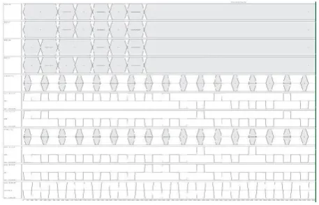
The coherence vector engine is used for simulations with the options shown in Table I. Layouts for the 16-, 32- and 64-bit versions of the novel adder are shown in Figs. 3–5, respectively. Simulation results for the 64-bit adder is shown in Fig. 6.There, the carry out bit is included in the output sum bus. Because of the limited
QCA Designer graphical capability, input and output busses are split into two separate more significant and less significant busses. Fig. 6 also shows the polarization values of few single output signals (i.e., sum64, sum32, sum31, and sum). Simulations performed on 32-and 64-bit adders have shown that the first valid result is outputted after five and nine latency clock cycles, respectively. As an example, the 20 clock phases (or five cycles delay) of the 32-bit adder are as follows: one clock phase is needed for inputs acquisition; the carry c2 related to the least significant bit positions is then
computed within the two subsequent clock phases; 15 phases are required for the carry propagation through the remaining bit positions; finally, two more phases are needed for the sum computation.
Critical path consistencies and post layout characteristics, such as cell count, overall size, delay, number of clock phases, and ADP, are shown in Table II for all the compared adders. The number of cascaded MGs with-in the worst case computational path directly impacts on the achieved speed performances as an MG always adds one more clock phase. However, it is worth not-ing that because of their different basic logics, designs with the same critical path can achieve different numbers of clock phases. As an example, the novel adder requires less clock phases than the CFA proposed in [16] to perform the generic addition operation. Table II shows that the layout strategy is also quite important.
In fact, designs using the same basic logic with the same worst case theoretical path can have different number of clock phases due to differently compact layouts.It should also be noted that the critical path of the HYBA
[14] contains the fewest MGs, while the novel adder, the RCA [13] and the CFA [12] require less additional clock phases exceeding the number of cascaded MGs.
This means that their layouts do not contain overlong wires, thus demonstrating that the novel architecture inherits logic advantages of CLA and parallel-prefix adders (i.e., the short computational path), but limiting, as happens in the RCA and CFA structures, detrimental layout effects. Comparison results shown in Table II for operands wordlengths ranging from 8- to 64-bit also show that the novel adder achieves the lowest delay and spans over an area similar to that occupied by the cheaper designs known in literature.
Therefore, our design approach allows the best area-delay tradeoff to be achieved. Table II also shows the numbers of wire crossovers for some competitors. As it is well known, wire crossovers are sensitive to fabrication imperfections and consequently they can represent a reliability issue [19]–[21]. It can be seen that the number of crossovers used in the novel 8- and 16- bit adder was 33.6% and 37% lower than the CLA and the BKA proposed in [15]. Unfortunately, for the adders
presented in [11]–[14], [16] similar information was not available. The robustness of the proposed circuit was evaluated as a function of temperature using a simulation set-up identical to that used in [13]. Obtained results demonstrated that at 22 K, all the out-put cells assume correct polarizations. In fact, the cells furnishing output signals equal to zero are polarized to
c e-ISSN: 2348-6848, p- ISSN: 2348-795X Volume 3, Issue 01, January 2016
International Journal of Research (IJR)
Available at http://internationaljournalofresearch.orgFig. 6. Simulation results obtained for the novel 64-bit adder.
V. CONCLUSION:
A new adder designed in QCA was presented. It achieved speed performances higher than all the exist-ing QCA adders, with an area requirement comparable with the cheap RCA and CFA demonstrated in [13] and [16]. The novel adder operated in the RCA fashion, but it could propagate a carry signal through a number of cascaded MGs significantly lower than conventional
RCA adders.
In addition, because of the adopted basic logic and lay-out strategy, the number of clock cycles required for completing the elaboration was limited. A 64-bit binary adder designed as described in this brief exhibited a delay of only nine clock cycles, occupied an active area of 18.72 μm2, and achieved an ADP of only 168.48.
REFERENCES:
[1] C. S. Lent, P. D. Tougaw, W. Porod, and G. H. Ber-nestein, “Quantum cellular automata,” Nanotechnol-ogy, vol. 4, no. 1, pp. 49–57, 1993.
[2] M. T. Niemer and P. M. Kogge, “Problems in design-ing with QCAs: Layout = Timdesign-ing,” Int. J. Circuit Theory Appl., vol. 29, no. 1,pp. 49–62, 2001.
[3] J. Huang and F. Lombardi, Design and Test of Digital Circuits by Quantum-Dot Cellular Automata. Norwood, MA, USA: Artech House, 2007.
[4] W. Liu, L. Lu, M. O’Neill, and E. E. Swartzlander, Jr., “Design rules for quantum-dot cellular automata,” in Proc. IEEE Int. Symp. Circuits Syst., May 2011, pp. 2361– 2364.
[5] K. Kim, K. Wu, and R. Karri, “Toward designing ro-bust QCA architectures in the presence of sneak noise paths,”
in Proc. IEEE Design, Autom. Test Eur. Conf. Ex-hibit., Mar. 2005, pp. 1214–1219.
[6] K. Kong, Y. Shang, and R. Lu, “An optimized major-ity logic synthesis methology for quantum-dot cellular automata,” IEEE Trans. Nanotechnol., vol. 9, no. 2, pp. 170– 183, Mar. 2010.
[7] K. Walus, G. A. Jullien, and V. S. Dimitrov, “Computer arithmetic structures for quantum cellular automata,” in Proc. Asilomar Conf.Sygnals, Syst. Comput., Nov. 2003, pp. 1435–1439.
[8] J. D. Wood and D. Tougaw, “Matrix multiplication using quantumdot cellular automata to implement conventional microelectronics,” IEEE Trans. Nanotech-nol., vol. 10, no. 5, pp. 1036–1042, Sep. 2011.
[9] K. Navi, M. H. Moaiyeri, R. F. Mirzaee, O. Hashemi-pour, and B. M. Nezhad, “Two new low-power full ad-ders based on majority-not gates,” Microelectron. J., vol. 40, pp. 126–130, Jan. 2009.
[10] [8] J. D. Wood and D. Tougaw, “Matrix multiplication using quantumdot cellular automata to implement conventional microelectronics,” IEEE Trans. Nanotech-nol., vol. 10, no. 5, pp. 1036–1042, Sep. 2011.
[11] [9] K. Navi, M. H. Moaiyeri, R. F. Mirzaee, O. Hashemi-pour, and B. M. Nezhad, “Two new low-power full ad-ders based on majority-not gates,” Microelectron.J., vol. 40, pp. 126–130, Jan. 2009.
[12] H. Cho and E. E. Swartzlander, “Adder design and analyses for quantum-dot cellular automata,” IEEE Trans. Nanotechnol., vol. 6, no. 3, pp. 374–383, May 2007.
[13] H. Cho and E. E. Swartzlander, “Adder and multi-plier design in quantum-dot cellular automata,” IEEE Trans. Comput., vol. 58, no. 6, pp. 721–727, Jun. 2009.
[14] V. Pudi and K. Sridharan, “Low complexity design of ripple carry and Brent–Kung adders in QCA,” IEEE
[15] Trans. Nanotechnol., vol. 11, no. 1, pp. 105–119, Jan. 2012.
[16] V. Pudi and K. Sridharan, “Efficient design of a hybrid adder in quantumdot cellular automata,” IEEE Trans. Very Large Scale Integr. (VLSI) Syst., vol. 19, no. 9, pp. 1535–1548, Sep. 2011.
c e-ISSN: 2348-6848, p- ISSN: 2348-795X Volume 3, Issue 01, January 2016
International Journal of Research (IJR)
Available at http://internationaljournalofresearch.orgthe design of efficient binary addition in QCA,” IEEE Trans. Nanotechnol., vol. 11, no. 6, pp. 1192–1200, Nov. 2012.
[18] V. Pudi and K. Sridharan, “New decomposition the-orems on majority logic for low-delay adder designs in quantum dot cellular automata,” IEEE Trans. Circuits
[19] Syst. II, Exp. Briefs, vol. 59, no. 10, pp. 678–682, Oct. 2012.
[20] K. Walus and G. A. Jullien, “Design tools for an emerging SoC technology: Quantum-dot cellular au-tomata,” Proc. IEEE, vol. 94, no. 6, pp. 1225–1244, Jun. 2006.
[21] S. Bhanja, M. Ottavi, S. Pontarelli, and F. Lombardi,
[22] “QCA circuits for robust coplanar crossing,” J.
Elec-tron. Testing, Theory Appl., vol. 23,no. 2, pp. 193–210, Jun. 2007.
[23] A. Gin, P. D. Tougaw, and S. Williams, “An alterna-tive geometry for quantum dot cellular automata,” J. Appl. Phys., vol. 85, no. 12,pp. 8281–8286, 1999.
[24] A. Chaudhary, D. Z. Chen, X. S. Hu, and M. T. Ni-emer, “Fabricatable interconnect and molecular QCA circuits,” IEEE Trans. Comput Aided Design Integr. Cir-cuits Syst., vol. 26, no. 11, pp. 1977–1991, Nov. 2007.
[25] M. Janez, P. Pecar, and M. Mraz, “Layout design of manufacturable quantum-dot cellular automata,” Mi-croelectron. J., vol. 43, no. 7, pp. 501–513, 2012