An Efficient FPGA-based Frequency Shifter for LTE/LTE-A Systems
Felipe A. P. de Figueiredo
Ghent University - imec, IDLab, Department of Information Technology, Ghent, Belgium.
Email: [email protected]
The Physical Random Access Channel (PRACH) plays an important role in LTE and LTE-A systems. It is through the PRACH channel that the user equipment (UE), based on eNodeB’s timing estimates, aligns its uplink transmissions to the eNodeB’s uplink and gain access to the network. One of the initial operations executed by the PRACH receiver at eNodeB side is the translation of the PRACH signal back to base band,i.e., center the PRACH signal around DC. This operation is a necessary step for pream-ble detection and can be carried out through a time-domain frequency shift operation. Therefore, in this paper we present the hardware architecture and implementation de-tails of a configurable and optimized FPGA-based time-domain frequency shifter. It is a hardware-efficient and accurate architecture for converting the relevant received PRACH signal into base band before further signal processing. The architecture is manly based on a customized Numerically Controlled Oscillator (NCO), which is used for generating complex exponentials employing only adders, a Look-Up Table (LUT) and plain logic re-sources. The main advantage of the proposed hardware architecture is that it completely eliminates the need for storing a large number of long complex exponential sequences by employing a single LUT and exploiting quarter wave symmetry of the basis waveform. Our simulation results show that the proposed customized NCO architecture provides high Spurious Free Dynamic Range (SFDR) signals using a minimal amount of FPGA resources. Moreover, the proposed architecture exhibits spur-suppression ranging from 62.13 to 153.58 dB without using Taylor Series correction.
Keywords: LTE, LTE-A, 4G, PRACH, NCO, time-domain frequency shift, FPGA
1. Introduction
Long Term Evolution (LTE) is the next step forward in cellular 3G services. LTE is a 3GPP standard that provides for an uplink speed of up to 50 megabits per second (Mbps) and a downlink speed of up to 100 Mbps. LTE brings many technical ben-efits to cellular networks. Bandwidth is scalable from 1.25 MHz to 20 MHz [1–4].
In order to make LTE a true 4th generation (4G) technology, it was enhanced to meet the IMT-Advanced requirements issued by the International Telecommu-nication Union (ITU). The necessary improvements are specified in 3GPP Re-lease 10 and also known as LTE-Advanced (LTE-A). LTE-A further increases peak data rates towards 1 Gbit/s in the downlink and 500 Mbit/s in the up-link. The technology components of LTE-A are Carrier aggregation, MIMO ex-tension (up to DL: 8x8; up to UL: 4x4), Uplink access enhancements (clus-tered SC-FDMA and simultaneous data and control information (PUSCH and PUCCH) transmission) and Improvement of cell edge performance by supporting
1
enhanced inter-cell interference coordination (eICIC) and Relay Nodes (RN) [3]. In LTE and LTE-A, uplink physical random access channel (PRACH) is used for initial access requests from the user equipment (UE) to the evolved base station (eNodeB) and to obtain time synchronization [3], [4]. In case of need to access the network, a UE requests access by transmitting a random access (RA) preamble through PRACH [5]. The RA preamble is then detected by the PRACH receiver at eNodeB side, which estimates both the ID of the transmitted preamble and the propagation delay between UE and eNodeB. Then, UE is time-synchronized according to a time alignment (TA) value (derived from the propagation de-lay estimate) transmitted from the eNodeB before the uplink transmission [6].
PRACH transmission opportunity is set by higher layers [7] and deter-mines the frequency-domain location of the random access preamble within the physical resource blocks. In this way, at eNodeB side, a fundamental op-eration before any attempt to detect random access preambles takes place is the extraction of relevant preamble signals through a time-domain fre-quency shift operation. This operation translates the PRACH signal from the frequency-domain location set by higher layers back to base band so that preamble detection can be totally carried out in base band [4].
This paper is an extension of a previous conference paper [8]. Differently from [8], where we provided only some very superficial aspects of the proposed algorithm and architecture, the current paper presents a meticulous analysis on its design and im-plementation aspects. Therefore, the main contributions of the current paper are (i) the design of a low computational complexity time-domain frequency shifter algorithm and hardware architecture to be employed in the PRACH receiver at eNodeB side; (ii) a thorough analysis of design and implementation details; (iii) discussion of the computational complexity of the proposed architecture in terms of FPGA resource utilization and speed; and (iv) careful analysis of the imple-mentation results considering spur-suppression, i.e., SFDR, SNR, probabilities of correct and error detection and average error between time-domain frequency shift operations carried out by a floating-point model, referred here as Golden Model (GM), and by the fixed-point FPGA implementation of the proposed architecture.
This paper contributes with a method and architecture optimized and tested for reduced complexity on a Xilinx Virtex 6 LX240T FPGA device. Results show that the architecture presents spur-suppression better than 62 dB and when it is employed in the PRACH receiver the probability of correct de-tection achieved by the receiver is greater than 99% at a SNR of -21 dB.
V. Finally, Section VI provides some concluding remarks.
2. Physical Random Access Channel
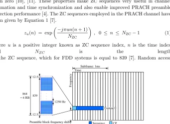
The PRACH is the physical channel that initiates communication with the eNodeB. It allows the eNodeB to calculate the time delay to the User Equipment (UE) and identify it prior to establishing a packet connection. To establish a connection with the eNodeB the UE initiates the random access procedure by sending a random access preamble using the PRACH. The physical layer random access preamble consists of a cyclic prefix and a sequence part as shown in [7] Table 5.7.1-1. This preamble is orthogonal to other uplink user data to allow the eNodeB do differen-tiate each UE. The subcarrier spacing for the PRACH is 1.25 KHz for formats 0 to 3, and 7.5 KHz for format 4. See example in Figure 1. Formats 0 to 3 are used for frame structure type 1,i.e., Frequency Division Duplexing (FDD) and Format 4 is used for the frame structure type 2, i.e., Time Division Duplexing (TDD) only [3]. As will be discussed later, the PRACH can be positioned at different fre-quency locations,i.e., RBs, depending on a parameter configured by higher layers. Figure 1 shows an example of a possible PRACH’s frequency-domain location.
Prime-length Zadoff-Chu (ZC) sequences are adopted as random access pream-bles in LTE and LTE-A systems due to its CAZAC properties,i.e., all points of the sequence lie on the unit circle and its auto-correlation is zero for all time lags other than zero [10], [11]. These properties make ZC sequences very useful in channel estimation and time synchronization and also enable improved PRACH preamble detection performance [4]. The ZC sequences employed in the PRACH channel have form given by Equation 1 [7].
zu(n) = exp
−jπun(n+ 1)
NZC
, 0 ≤ n ≤ NZC−1 (1)
where u is a positive integer known as ZC sequence index, n is the time index
and NZC is the length
of the ZC sequence, which for FDD systems is equal to 839 [7]. Random access
! " #$
%%&'
( (
preambles with zero correlation zones are defined from theu-th root ZC sequence. This sequence length, NZC, corresponds to approximately 69.92 Physical Up-link Shared Channel (PUSCH) subcarriers in each SC-FDMA symbol, and of-fers a band protection of 72−69.92 = 2.08 PUSCH subcarriers, which corre-sponds to approximately one PUSCH subcarrier protection on each side of the preamble [7]. PUSCH sub-carriers are spaced 15 KHz apart from each other.
The PRACH occupies a bandwidth of 1.08 MHz that is equivalent to 6 Resource Blocks (RB). Differently from other uplink channels, PRACH uses a subcarrier spacing of 1250 Hz for preamble formats 0 to 3 [7]. The ZC se-quence is specifically positioned at the center of the 1.08 MHz bandwidth, i.e., at the center of the block of 864 available PRACH subcarriers, so that there is a guard band of 15.625 KHz on each side of the preamble, which corre-sponds to 12.5 null PRACH subcarriers. These guard bands are added to PRACH preamble edges in order to minimize interference from PUSCH. Figure 1 de-picts the PRACH preamble mapping according to what was just exposed.
The PRACH sequence, which for formats 0 and 1 is 800 us long, is created by cyclically-shifting a root ZC sequence of prime-lengthNZC, defined as in Equa-tion 1. Random access preambles with zero correlaEqua-tion zones of length NCS−1 are generated by applying cyclic shifts to theu-th root ZC sequence, according to Equation 2.
xu,v(n) =xu((n+Cv)modNZC) (2) where v is the sequence index and Cv is the cyclic shift applied to the root ZC sequence and calculated asCv =vNCS for unrestricted sets [7]. Parameter NCS gives the fixed length of the cyclic shift. All the possible values for these parameters are defined in [7].
2.1. PRACH Receiver
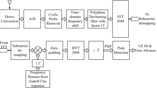
In the literature there are two approaches for PRACH receivers, the full frequency-domain one and the hybrid time/frequency domain one [4, 9]. Al-though the full frequency-domain approach provides the optimal detection per-formance, this approach uses considerably large size discrete Fourier transform (DFT), to be more precise a 24576-point DFT. On the other hand, the hy-brid time/frequency domain approach uses FFT/IFFT blocks of the same size, i.e., 2048-point FFT when the decimation factor adopted is 12. Thus, the hy-brid time/frequency domain substantially reduces the complexity of the hard-ware implementation. Therefore, in order to reduce the implementation com-plexity of the PRACH receiver we adopt the hybrid time/frequency domain ap-proach, which results in more practical implementations [4]. Figure 2 depicts the PRACH receiver architecture implemented and being used in our L1 solution.
block, multiplied by a Fourier transformed root Zadoff-Chu (ZC) sequence and then the resulting sequence is searched for peaks above a predefined threshold which is calculated to produce a given probability of false alarm. Figure 2 depicts the main components of the PRACH receiver at eNodeB side, for further details refer to [12].
The first block in Figure 2 is the Cyclic Prefix remover, which discards all sam-ples from the CP part of the preamble. Next, the PRACH pass-band signal is shifted to base-band by multiplying it with a complex exponential. In the sequence, the base-band signal is fed into a decimator block, which decimates the signal by a factor of 12, now instead of 24576 samples in the case of format-0 we have only 2048 samples. The FFT engine transforms the SC-FDMA symbols from time do-main into frequency dodo-main. The sub-carrier de-mapping block extracts the RACH preamble sequence from the correspondent FFT bins. The result of sub-carrier de-mapping is multiplied by the root ZC sequence and then fed into a zero-padding block. Finally, the IFFT engine is used to produce the cross-correlation between the root ZC sequence and the received preamble signal. All samples coming out of the IFFT block have their square modulus calculated producing what is known as Power Delay Profile (PDP) samples. Finally, the preamble detection block employs the PDP samples to estimate the noise power, set a detection threshold and then decides whether a preamble is present or not. As output of the detection process this block reports to the MAC layer all detected preambles and its respective Time Advance (TA) estimates. For further information on this receiver architecture and detection algorithm, refer to [4], [12].
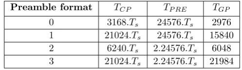
2.2. Preamble Format
The PRACH preamble, illustrated in Figure 3, consists of three parts: a Cyclic Prefix (CP) with length TCP, which is added to the preamble in order to ef-fectively eliminate Inter Symbol Interference (ISI), a signature or sequence part of length TP RE and of a guard period TGP which is an unused portion of time
! "#
$%
&
"
&
'()
*
+
,-*. /#
$%
# /0
!!
"#$%&'
()*+,*-(+*
Figure 3. Random Access Preamble Format 0.
at the end of the preamble used for absorbing the propagation delay. The stan-dard defines four different preamble formats for FDD operation [7]. Parame-ters TP RE, TCP and TGP are set according to the chosen preamble format.
Figure 3 shows the parameter values for format-0 and the values for all formats are listed in Table 1 whereTs is known as the standard time unit which is used throughout the LTE specification documents. It is defined asTs= 1/(15000x2048) seconds, which corresponds to a sampling rate of 30.72 MHz.
2.3. PRACH Preamble Signal
The PRACH preamble signals(t) can be defined as follows [7]:
s(t) =βP RACH NZC−1
X
k=0
NZC−1 X
n=0
xu,v(n).exp
−j2πnk
NZC
.exp [j2π[k+ϕ+K(k0+ 1/2)] ∆fRA(t−TCP)]
(3)
where 0 ≤ t < TP RE +TCP, βP RACH is an amplitude scaling factor and k0 =
nRA
P RBNSCRB−NRBU LNSCRB/2. The location in the frequency domain is controlled by the parameternRAP RB also known asnRAP RB
of f set, (it is the inputf requency of f set i of the Time Domain Frequency Shifter module) expressed as a resource block num-ber configure by higher layers and fulfilling 0≤nRAP RB ≤NRBU L−6, this inequality is only valid for formats 0, 1 2 and 3, i.e., FDD. The factor K = ∆f /∆fRA ac-counts for the ratio of subcarrier spacing between the PUSCH and PRACH and it is equal to 12 as ∆f = 15 KHz and ∆fRA = 1250 Hz. The variable ϕ (equal to 7 for LTE FDD) defines a fixed offset determining the frequency-domain location
Table 1. Random Access Preamble Formats
Preamble format TCP TP RE TGP
0 3168.Ts 24576.Ts 2976
1 21024.Ts 24576.Ts 15840
2 6240.Ts 2.24576.Ts 6048
of the random access preamble within the resource blocks. NU L
RB is the uplink sys-tem bandwidth (in RBs) and NRB
SC is the number of subcarriers per RB, i.e. 12. By noticing that the inner summation is the DFT ofxu,v(n) of lengthNZC we can rewrite equation 3 the following way:
s(t) =βP RACH NZC−1
X
k=0
Xu,v(k).exp [j2πk∆fRA(t−TCP)] .exp [j2π(ϕ+K(k0+ 1/2)) ∆fRA(t−TCP)]
(4)
Again, by noticing that the first part of the summation in 4 is a time shift applied to the DFT of xu,v(n) we can rewrite that first part of the equation as follows by replacing tby ∆t, which is referred in [7] as the standard time unitTs, i.e., the sampling rate.
s(t) =βP RACH NZC−1
X
k=0
Xu,v(k)
.exp [j2πk∆fRA∆t(n−NCP)]
(5)
where NCP is the number of samples corresponding to the CP interval as shown in Figure 3 and ∆fRA∆t = 1/NP RE (where for formats 0 ad 1,NP RE = 24576). Then rewriting equation 5 we have
s(t) =βP RACH NZC−1
X
k=0
Xu,v(k).exp
j2πk(n−N
CP) NP RE
=βP RACH.x,u,v(n−NCP)
(6)
Therefore as it can be easily seen the result of the above equation is nothing more than the application of the DFT’s time-shift theorem. It is also easy to see that this equation is the IDFT of Xu,v(k) with lengthNP RE. With that in mind equation 4 can be rewritten as
s(t) =βP RACH.x,u,v(n−NCP) .exp
j2π(ϕ+K(k
0+ 1/2)) (n−NCP)
NP RE
(7)
Equation 4 can be reorganized the following way s(t) =βP RACH.exp
−j2πNCP(ϕ+K(k0+ 1/2))
NP RE
.
x,u,v(n−NCP).exp
j2πn(ϕ+K(k
0+ 1/2))
NP RE
(8)
The part of equation 8 between curly braces represents a circular frequency shift applied tox,u,v(n−NCP),i.e.,
x,u,v(n−NCP).exp
j2πnm
NP RE
DF T
wheremis the frequency shift applied to the PRACH signal before it is transmitted and it is given by the following equation
m=ϕ+K(k0+ 1/2) (10)
Once we are only dealing with FDD, equation 10 can be further simplified as m= 13 + 144nRAP RB−72NRBU L (11) Therefore, at the PRACH receiver side, after removing CP and GP the preamble is still shifted in frequency-domain by an offset factor given by m. For further processing, it is necessary to convert the shifted preamble into base-band. This conversion is performed by the Time-domain frequency shift module (see figure 2), which multiplies the received preamble by the conjugate of the complex exponential term given in equation 9.
3. Efficient Algorithm of a Time-Domain Frequency Shifter
In this section, we present an efficient algorithm used to apply frequency-domain shifts to random access preamble signals in time-domain (i.e., without the need to convert them to the frequency-domain) through the use of a customized NCO and a complex multiplier. We also discuss the advantage presented by the proposed algorithm.
3.1. Numerically Controlled Oscillator
Numerically controlled oscillators (NCO), are important components in many digital communication systems. They are generally employed in quadrature synthesizers, which are used for constructing digital down and up convert-ers, demodulators and here for time-domain frequency shifters. A common method for digitally generating complex or real valued sinusoids employs a look-up table (LUT) scheme [14]. The LUT stores samples of a sinusoid.
A digital integrator is used to generate a suitable phase argument that is mapped by the LUT to the desired output waveform. The in-tegrator computes a phase slope that is mapped to a sinusoid (possi-bly complex) by the LUT. This value is presented to the address port of the LUT that performs the mapping from phase-space to time [15].
The LUT traditionally stores uniformly spaced samples of a cosine and a sine wave. These samples represent a single cycle of a length N = 2BΘ(n) prototype
complex sinusoid and correspond to specific values of the sinusoid’s argument Θ(n) as shown in Equation 12.
Θ(n) =n2π
N (12)
wherenis the time series sample index andBΘ(n) is the number of bits employed
in the phase accumulator which is calculated as shown in Equation 13. BΘ(n)= log2
f
clk ∆f
where d.edenotes the ceiling operator, fclk is the system clock frequency and ∆f is the frequency resolution of the NCO. The frequency resolution, ∆f, of the NCO is a function of fclk and BΘ(n). Then ∆f can be determined using the following
equation
∆f = fclk 2BΘ(n) =
fclk
N (14)
The output frequency,fout, of the NCO waveform is a function of fclk,BΘ(n)
and the phase increment value ∆θ. That is,fout =f(fclk, BΘ(n),∆θ) which is given
in Hertz and is defined in Equation 15. The phase increment, ∆θ is an unsigned value which defines the NCO output frequency.
fout= fclk∆θ 2BΘ(n) =
fclk∆θ
N (15)
The fidelity of a signal formed by recalling samples of a sinusoid from a LUT is affected by both the phase and amplitude quantization of the process. The length and width of the LUT affect the signal’s phase angle resolution and the signal’s amplitude resolution respectively. These resolution limits are equivalent to time base jitter and to amplitude quantization of the signal, and add spectral mod-ulation lines and a white broad-band noise floor to the signal’s spectrum [16].
Quarter wave symmetry in the basis waveform can be exploited to construct a NCO that uses shortened tables. We will discuss this approach next.
3.2. Iterative Time-Domain Frequency Shift Algorithm
The optimized algorithm representing the Time Domain Frequency Shift
opera-tion is presented in Algorithm
1. It depicts the data processing executed by each one the units in Figures 4. At first, during eNodeB’s initialization, the parametersof f set andbandwidth (bw) are sent by higher layers to the PHY which in turn feeds them into the Time Domain Frequency Shifter module so that the Discrete Frequency Shift Calculator unit is able to calculate the actual frequency shift to be applied to the received PRACH signal. Whenever a subframe in which random access preamble transmis-sions are allowed happens (it is set according to Table 5.7.1-2 in [7]) and after CP is removed the Customized NCO unit generates a complex exponential sig-nal with frequency set earlier by the Discrete Frequency Shift Calculator unit and multiplies it sample-by-sample with the incoming PRACH complex signal sam-ples, note that it is a complex multiplication once both are complex signals.
shown in Algorithm 1 once it mapsthetainto a value of a 1/4-length cosine table. In the light of what was presented in the previous section we now discuss the Algorithm 1. The first part of the algorithm is responsible for calculating the dis-crete frequency of the complex exponential signal that the NCO must generate in order to shift the received pass-band preamble signal to base-band. The discrete frequency shift, m, is calculated as shown in Equation 11. By remembering that ∆fRA∆t= 1/NP RE and then rewriting the exponential part of Equation 9 as
exp [j2π(m∆fRA)t] (16)
By analyzing the equation above it is noticeable that all frequency shifts are integer multiples of ∆fRA and this way we state that the output frequency of the NCO must be fout = m∆fRA. Before proceeding we must define the values for some parameters presented in the previous section. The frequency resolution ∆f = ∆fRA = 1250Hz, the system clock frequency fclk = 1/Ts = 30.72MHz, the length,N = 2BΘ(n) of the single cycle of the basis complex waveform is made
equal to 24576 samples. The cycle length can be expressed as N = fclk/∆fRA. Then, using the aforementioned definitions and rewriting Equation 15 letting ∆θ in evidence we have:
∆θ=foutN fclk =
m∆fRAN fclk =m
∆fRA fclk
fclk
∆fRA =m (17)
In case m is negative it is necessary to calculate its module in relation to NP RE before feeding it into the customized NCO. Note in Algorithm 1 that the module operation is simply done by adding NP RE to the negative value of m.
In a traditional NCO algorithm, i.e., one that adopts full-period wave-forms, there would be two main parts, namely, Phase Accumulator and LUT. In its simplest form, there would be 2 LUTs storing samples of a cosine and a sine wave. However, this approach generally results very large tables, which sometimes are impractical. Therefore, for a practical implementation with re-duced tables, the proposed algorithm employs only one LUT exploiting quarter-wave symmetry in the basis quarter-waveform and the constant phase offset (pi/2) between sine and cosine signals. In this approach we use one LUT with N/4 samples. However, when exploiting quarter-wave symmetry the mapping from phase-space to time is not direct as in the traditional NCO algorithm.
In order to exploit quarter-wave symmetry it is needed an algorithm to map the angle values (phase-space),θ, output by the phase accumulator into valid positions of a shortened LUT containing the samples of a cosine signal. This task is performed by the Angle Mapper part of Algorithm 1. The Angle Mapper maps angle values in the 2nd, 3rd and 4th quadrants into the 1st one and tracks the signals that must be applied to cosine and sine values. As can be seen in Algorithm 1 the indices for generating the cosine signal are calculated first and then aN/4-phase offset, which is equivalent to api/2 offset, is applied to it in order to generate the sine indexes.
Algorithm 1Time Domain Frequency Shifter Algorithm
1: procedureTDFreqShifter(re ad, im ad, of f set, bw, cos table)
2:
3: .********* Discrete Frequency Shift Calculator ********* 4: m= 13 + 144∗of f set−72∗bw;
5: . Frequency Control Word (FCW) —-6: delta theta=m;
7: ifm <0then
8: delta theta=N+m;
9: end if
10:
11: .************* Customized NCO Algorithm ************ 12: theta= 0;
13: fori←0to N−1do
14: . Angle Mapper —-15: cos signal= 1; 16: sin signal= 1;
17: iftheta >3∗N/4then
18: cos idx= (N−theta);
19: else
20: iftheta > N/2then
21: cos idx= (theta−(N/2)); 22: cos signal=−1;
23: else
24: iftheta > N/4then
25: cos idx= ((N/2)−theta); 26: cos signal=−1;
27: sin signal=−1;
28: else
29: cos idx=theta;
30: sin signal=−1;
31: end if
32: end if
33: end if
34:
35: sin idx= (N/4)−cos idx; 36:
37: ifcos idx==N/4then
38: cos idx= ((N/4)−1);
39: end if
40: ifsin idx==N/4then
41: sin idx= ((N/4)−1);
42: end if
43:
44: . Phase to Value Mapping (LUT) —-45: re nco(i) =cos signal∗cos table(cos idx); 46: im nco(i) =sin signal∗cos table(sin idx); 47:
48: . Phase Increment (Phase Accumulator) —-49: theta= (theta+delta theta);
50: iftheta >=N then
51: theta= (theta−N);
52: end if
53:
54: .*************** Complex Multiplier *************** 55: re bb(i) =re ad(i)∗re nco(i)−im ad(i)∗im nco(i); 56: im bb(i) =re ad(i)∗im nco(i) +im ad(i)∗re nco(i);
57: end for
58: returnre bb, im bb
zero. The zero value can be mapped to the value stored at the N/4-th po-sition with minimal degradation on SFDR performance. Therefore, as can be seen in the algorithm, when either sine or cosine indexes are equal to N/4 their values are changed to (N/4) −1, which is the closest value to zero.
As the LUT only stores samples from the 1st quadrant of a cosine signal,i.e., only positive values, the Phase to Value Mapper part of the algorithm must ap-ply the correct signals (provided by the Angle Mapper) to the LUT’s output.
The Phase Increment (also referred as Phase Accumulator) part of the algo-rithm acts as an integrator. It calculates at each iteration of the algoalgo-rithm a new phase value, θ, by using the phase increment ∆θ value provided by the Discrete Frequency Shift Calculator part. Once the Angle Mapper algorithm can only map values ranging from 0 toN−1 into the range 0 to (N/4)−1 it is necessary to apply a module operation in case the resulting phase value is equal or greater than N. The module operation is easily performed by subtractingN from the phase value.
The last part of the algorithm multiplies sample-by-sample the generated com-plex exponential signal by the ADC signal. That comcom-plex multiplication operation then translates the pass-band PRACH signal into base-band.
3.3. Advantage of the Proposed Algorithm
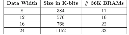
The main advantage of the proposed algorithm is the memory savings attained by the use of a 1/4-length cosine table instead of storing in RAM each one of the 2N possible samples of a complex exponential signal. Table 2 shows the memory utilization for some data widths if we were to store all the 2N samples (sine and cosine waves) corresponding to one complete period of the basis complex exponen-tial waveform necessary to translate the received PRACH signal into base band.
In Xilinx FPGAs, a Block RAM (BRAM) is a dedicated, i.e., they cannot be used for anything but RAM, two-port memory containing several kilobits of RAM. A FPGA contains a limited number of these blocks. The configuration logic blocks (CLB) in most of Xilinx FPGA’s contains a small RAM. They are called distributed (LUT) RAM because they are distributed throughout the FPGA once they are part of a CLB. This kind of RAM can normally store only a dozen bits.
A reasonable rule of thumb when designing with FPGAs is that if you need a lot of RAM, as is the case here, you should use BRAMs, otherwise the FPGA resources will be eaten up implementing the RAM in distributed RAM. It is
im-Table 2. Memory utilization when storing the full period of the complex exponential.
Data Width Size in K-bits # 36K BRAMs
8 384 11
12 576 16
16 768 22
Table 3. Memory utilization when employing quarter-wave symmetry.
Data Width Size in K-bits # 36K BRAMs Reduction in %
8 48 2 81.8
12 72 2 87.5
16 96 3 86.4
24 144 4 87.5
portant to say that a Virtex-6 FPGA device has only 416 36K-bits BRAMs which makes it a very precious resource when implementing a large project as a L1 PHY and in this way its usage must be taken into account during planning and develop-ment. One alternative to decrease the number of occupied BRAMs is the exploita-tion of quarter-wave symmetry in the basis waveform. This alternative results in a customized NCO that employs a shortened LUT. As can be seen in Table 3.
The fourth column in Table 3 shows the reduction of used BRAMs when ex-ploiting quarter-wave symmetry. As can be noticed, this approach results in a more area efficient implementation because the memory requirements are minimized,i.e., fewer FPGA BRAMs are required. Therefore this approach saves on valuable chip area and also reduces power consumption.
4. Implementation Details
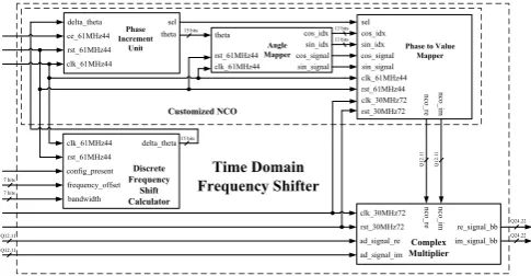
This section presents some discussions on implementation details of the pro-posed architecture. It is suitable for implementation on devices that em-ploy hardware description language (HDL) as part of its design process such as Field Programmable Gate Arrays (FPGA) and Application Spe-cific Integrated Circuits (ASIC). Figure 4 shows the hardware architecture of the Time-domain Frequency Shifter module. The architecture employs only one LUT and exploits quarter wave symmetry for shortened tables.
The architecture works with two different system clocks, the first one of 30.72 MHz, is the clock used by the ADC unit and therefore dictates the rate the
!" !#$ %!! &
!"
plex multiplication must be carried out. Only two units run at this rate, namely, Complex Multiplier and Phase to Value Mapper. The second system clock, 61.44 MHz, is employed so that 2 samples of the complex exponential can be retrieved from the same LUT within the period of one sample coming from the ADC. This double system clock mechanism further reduces the amount of RAM needed. All units run at this rate with only one exception, the Complex Multiplier unit.
The input parametersf requency of f setandbandwidthare fed into the module only when the eNobeB is being initialized. They can be considered static parameters of a eNodeB. The input signalconf ig presentis asserted by higher layers during the initialization process to inform when the input parameter values are valid.
The Time-domain Frequency Shifter module needs to be informed by means of the ce 61M Hz44 signal when the sequence part of the preamble starts so that it can be multiplied by the complex exponential the Customized NCO unit gen-erates. Signal ce 61M Hz44 is asserted by the PRACH receiver module after it discards the CP part of the preamble and must stay high for the whole duration of the sequence part, for example, for format-0 it must stay high for 24576 30.72 MHz-clock cycles, i.e., 2*24576 when the 61.44 MHz system clock is considered. Once all units have registered outputs some latency is expected and then must be accounted for by the PRACH receiver when asserting the chip enable signal.
Other characteristic of the architecture is that it uses a total of 4 multipliers which are employed in the Complex Multiplier unit. Besides that, the architecture only employs bit-shift and add operations to eval-uate trigonometric functions, i.e., complex exponentials, turning it into a very efficient hardware architecture in terms of logic resource usage.
The proposed architecture can have its outputs and inputs totally configured, i.e., input and output widths can be configured for one the following options: 8, 12, 16 and 24 bits. In our case we are using an ADC which outputs 12 bits for each one of the quadrature components I and Q and has fixed-point representation (Q Format) Q12.11,i.e., 1 integer bit and 11 fractional bits. The quadrature compo-nents of the complex exponential generated by the Customized NCO have the same fixed-point representation of the input. In this regard, after the complex multipli-cation between ADC and NCO quadrature samples which involves multiplimultipli-cation and subsequent addition, the fixed-point representation of the output is Q25.22. As the maximum possible value produced by the complex multiplication operation is 2 the integer part only needs 2 bits instead of 3. In this way, depending on the configuration the fixed-point representation of the output complex signal can be set to Q8.6, Q12.10, Q16.14 and Q24.22.
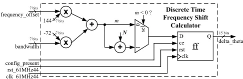
4.1. Discrete Frequency Shift Calculator Unit
!
" ! #
$ %
&
Figure 5. Architecture of the Discrete Frequency Shift Calculator unit.
Equation 11. All multiplications are performed through bit-shifting the input values nRA
P RB and N U L
RB by the constant values 144 and -72 respectively and then adding the result to the constant 13. Before feeding m into the Customized NCO unit it is necessary to check if the resulting value is negative, if so, the constant value N is summed to the resulting value then turning m into a positive value. It is done because the Phase Increment Unit composing the Customized NCO expects only positive values. As shown in Equation 17 the discrete frequency shift,mis equal to ∆θthat is the input value necessary for the Customized NCO to operate.
4.2. Customized Numerically Controlled Oscillator
As can be seen in Figure 4 the Customized Numerically Controlled unit is made up of three blocks, namely, Phase Increment, Angle Mapper and Phase to Value Mapper. The first two units operate at 61.44 MHz and the last one operates at 30.72 and 61.44 MHz as it is the unit responsible for retrieving both quadrature values I and Q from the LUT within one period of the 30.72 MHz system clock.
Figure 6 shows the architecture of the Phase Increment unit. This unit im-plements a digital integrator which generates the phase argument, θ, fed into the Angle Mapper unit. At each iteration ∆θis added toθ which starts with 0. If the resulting θ value is greater than N + 1 the constant value−N is added to it so that it stays less than N and thus can be correctly mapped into a valid value. This procedure is the direct implementation of a module operation, mod(θ, N). The unit only outputs a valid θ value when the selection, sel, signal is asserted. The sel signal is generated by a clock divisor which divides the 61.44 MHz clock by 2, i.e., the unit outputs a valid value at a rate of 30.72 MHz. The selection signal is also output by the unit in order to feed the Phase To Value Map-per unit. As Equation 13 is equal to N and it is not a power of 2, the data width of the Phase Increment unit, BΘ(n), should be ceiled, resulting in 15 bits.
not stored in the LUT whenever either cosine or sine indexes are equal to N/4 their values are changed to (N/4) −1, which is the closest value to zero.
The unit is also in charge of tracking the signals that must be applied to the quadrature values I and Q at the output of the Phase to Value Mapper unit. These signals translate the phase argument, represented by the cosine and sine indexes, back to its original quadrant. At the input of this unit the phase argument,θ, has a data width of 15 bits so that it could accessN samples, i.e., all the four quad-rants, however, as the Angle Mapper unit translatesθto the first quadrant the data width can be reduced to 13 bits that is the number of bits necessary to access the N/4 samples of the 1st quadrant (quarter wave symmetry) and which are stored in the LUT. It runs at 61.44 MHz and generates two new indexes, cosine and sine, at a 30.72 MHz rate once the phase argument θ is fed into the unit at that rate.
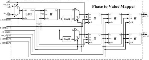
Figure 8 shows the architecture of the Phase to Value Mapper unit which is responsible for the mapping from phase-space to time. The cosine and sine indexes are used as addresses to access positions of the LUT. It is the LUT that performs the translation from phase-space to time. The LUT stores only 1/4, i.e., N/4, of the cosine signal used as basis waveform. The selection,sel, signal chooses whether cosine or sine index is used to read the LUT. As can be seen in Figure 8 the co-sine index is used as address whensel is low and the sine index when it is high.
Both cosine and sine indexes stay constant for a 30.72 MHz clock cycle. As the LUT operates at a rate of 61.44 MHz and both indexes are simultaneously present at its input it is possible to retrieve 2 samples within one period of the 30.72 MHz clock. By creating a delayed data path (with the use of a register) at the output of the LUT it is possible to divert the in-phase (I) and quadra-ture (Q) samples to two different data paths and thus generating the complex exponential necessary to shift the received PRACH preamble to base band. At this point, the generated quadrature signal is synchronized to the 61.44 MHz sys-tem clock, however, each quadrature pair lasts for one period of the 30.72 MHz
Figure 7. Architecture of the Angle Mapper unit.
system clock. It is explained by the two registers with chip enable inputs driven by the sel signal positioned at the output of the signal changing multiplexers.
In order to translate the quadrature samples to their original quadrants the cosine and sine signals generated by the Angle Mapper unit are ap-plied to their respective data paths. The signal change when due is eas-ily performed by applying the two’s complement to the sample value.
Finally, as the ADC has a data rate of 30.72x10⁶samples per second it is
neces-sary to change the clock domain of the complex exponential signal, even tough its samples lasts for the correct period, they are not synchronized to the 30.72 MHz system clock. A simple way to perform this crossing of clock domains is to em-ploy two registers at the desired clock rate. As we have a complex signal we use a pair of double registers for each of the quadrature components. Now the complex
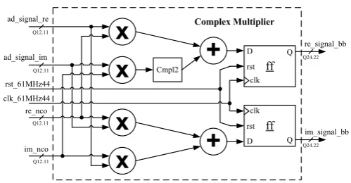
Figure 9. Architecture of the Complex Multiplier unit.
exponential signal is ready to be multiplied by the incoming PRACH preamble.
4.3. Complex Multiplier Unit
Figure 9 depicts the architecture devised for the Complex Multiplier unit. Once samples coming from both NCO and ADC are complex, it is necessary a complex multiplier to multiply then and perform the necessary frequency shift in time do-main. The complex multiplier or also known as mixer multiplies the ADC samples, i.e., the PRACH signal, by the complex exponential samples generated by the Cus-tomized NCO unit. The multiplication of two complex numbers,a+jbandc+jd, results in the complex product given by Equation 18.
real+j∗imag= (a+j∗b)∗(c+j∗d)
= (ac−bd) +j∗(ad+bc) (18) As can be realized, the complex multiplication requires 4 multiplications and 2 additions once we consider a subtraction as being an addition in 2’s complement. The Complex Multiplier unit operates at the system clock of 30.72 MHz once we must always respect the data rate dictated by the ADC.
5. Simulation and Implementation Results
In order to assess the efficiency of the Customized NCO and Time Domain Fre-quency Shifter units proposed in this paper some simulations were carried out. The proposed Time Domain Frequency Shifter architecture was developed in VH-SIC Hardware Description Language (VHDL) and a corresponding bit-accurate Matlab model, referred here as Golden Model (GM), was developed for verifi-cation. The full design was targeted to a Xilinx Virtex 6 xc6vlx240t FPGA.
−6000 −4000 −2000 0 2000 4000 6000 10−8
10−7 10−6 10−5 10−4 10−3 10−2
Discrete Frequency − m
Average Error Q8.7
Q12.11 Q16.15 Q24.23 Q32.31
Figure 10. Average error between GM and DUT implementations of the Customized NCO.
5.1. Customized Numerically Controlled Oscillator
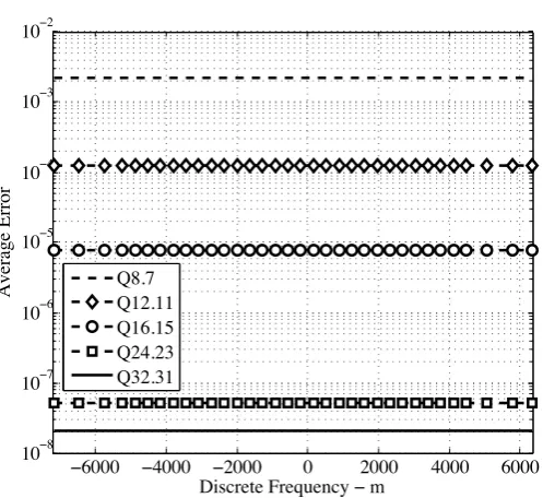
This section presents results regarding the Customized NCO implementation. The first simulation result, showed in Figure 10, compares floating-point cision Matlab generated complex exponential sequences with fixed-point pre-cision sequences generated by the device under test (DUT) along all pos-sible discrete frequency shifts, m, and for some Q-formats. PRACH format-0 preambles were considered for this and all other simulation results.
Figure 11 presents the SFDR variation of the implemented NCO unit, i.e., the DUT, along all possible discrete frequency shifts, m and for some Q-formats. SFDR is the power ratio between the fundamental signal and the strongest spurious signal,i.e., the most prominent harmonic, present at the output of the Customized NCO. By analyzing this result it is noticeable that the SFDR attained by the DUT is almost the same for formats Q24.23 and Q32.31. The SFDR values achieved by the DUT for formats Q24.23 and Q32.31 are 153.58 and 154.2 dB respectively. These high SFDR values are due to the fact that the phase increment bits are not truncated and all output frequencies, fout, are integer multiples of the system clock frequency, fclk, which is the frequency used to sample the basis waveform, and therefore, eliminating the spectral artifacts resultant from phase jitter [16].
format Q8.7. The noise floor for format Q24.23 is so small that it is imperceptible. Figure 13 depicts the SNR variation of the Customized NCO along all possible discrete frequency shifts,mand for some Q-formats. The SNR results are obtained by the ratio between the signal average power and the noise average power.
5.2. Time Domain Frequency Shifter
This section presents results regarding the implementation of the Time Domain Frequency Shifter architecture. From this point on we refer to the architecture im-plementation as the DUT. This time a Matlab floating-point model (GM) of the whole Time Domain Frequency Shifter architecture is used to assess the
perfor-mance of the circuit.
Table 4 presents information on the resource utilization of the pro-posed time domain frequency shifter. It summarizes the main results ob-tained from the implementation of the proposed architecture on a FPGA device. The number of registers, occupied slices, LUTs, memory resources and Digital Signal Processor (DSP) resource blocks are presented. The maximum operation frequency reached by the module is 239.981 MHz.
From the results of Table 4, it can be noticed that 3 Block RAM (BRAM) memories are used instead of the 2 mentioned earlier. The synthesis tool maps the content of the LUT to 3 BRAMs because the number of bits used to ad-dress the LUT is 13, therefore, ceil((213∗12)/36K) = 3 instead of 2. Note that
each position of the BRAM stores a 12-bit value sampled from the basis wave-form. The 4 instantiated xilinx’s DSP48 resources are employed by the
Com-−6000 −4000 −2000 0 2000 4000 6000
60 70 80 90 100 110 120 130 140 150
Discrete Frequency − m
NCO’s SFDR variation [dB]
Q8.7 Q12.11 Q16.15 Q24.23 Q32.31
−1 0 1 x 10⁷
−150
−100
−50
SFDR: 62.13 dB Q8.7
Frequency [Hz]
Power [dBm]
−1 0 1
x 107
−160
−140
−120
−100
−80
−60
−40
−20
SFDR: 96.52 dB Q12.11
Frequency [Hz]
Power [dBm]
−1 0 1
x 107
−150
−100
−50
SFDR: 124.14 dB Q16.15
Frequency [Hz]
Power [dBm]
NCO Power Spectrum
−1 0 1
x 107
−150
−100
−50
SFDR: 153.58 dB Q24.23
Frequency [Hz]
Power [dBm]
Figure 12. Customized NCO Power Spectrum.
plex Multiplier unit to implement the multiplication shown in equation (18).
In Virtex
6 family, 1 slice corresponds to 4 LUTs and 8 flip-flops. Block RAM/FIFOs are embedded resources of 36-bit memory. DSP48 is an embedded processing resource
−6000 −4000 −2000 0 2000 4000 6000 90
100 110 120 130 140 150 160
Discrete Frequency − m
NCO’s SNR variation [dB]
Q8.7 Q12.11 Q16.15 Q24.23 Q32.31
equivalent to 1 multiplier with two 18-bit inputs and one accumulator of 48 bits. The reuse of DSP48 resources is a feasible strategy that can further optimize FPGA area at the expense of an increased clock operation and additional control logic. For example, the four full-parallel multiplications present in the Complex Multiplier unit can be serialized saving 3 out of the 4 DSP48 already in use.
As can be noticed by analyzing Table 4, the proposed architecture occupies less than 1% of all Virtex 6 logic resources. The use of low cost FPGAs is allowed once the implementation of the proposed architecture on FPGA presents a very low oc-cupancy rate. There are two points to take into account when choosing a low-cost FPGA: 1) the maximum achievable frequency, since low-cost FPGAs tend to have worse timing characteristics and 2) slice count could increase for technologies below Virtex-6, once other families may use 4-bit LUT instead of the 6-bit LUT per slice.
Figure 14 shows the average error between frequency shifted preambles produced by the GM and DUT. In order to get a concise plot the average error for a given preamble is averaged over all possible offsets applied to that preamble,i.e., the figure presents the average of the average error over all possible offsets applied to a given preamble. The figure shows the average error for some Q-formats when the band-width parameter,NRBU L, is set to 25 and 50 RBs,i.e., bandwidths of 5 and 10 MHz respectively, and the offset parameter, nRA
P RB, is varied along all possible values. Figure 15 shows an exploded view of the results presented in Figure 14. Each subplot, representing the error for a specific Q-format, depicts the average of the average error over all possible offsets applied to a given preamble for 25 and 50 RB bandwidths. It is clearly seen that the er-ror has a very small variation, almost constant, along the preambles.
Next we present results regarding the use of the Time Domain Frequency Shifter architecture proposed in this work in the context of the PRACH receiver at eN-odeB PHY side. The PRACH receiver architecture adopted in this work is shown in Figure 2 and a bit-accurate Matlab model was developed for its verification.
At the receiver side, the eNodeB attempts to detect a transmitted preamble by first extracting the PRACH signal from a received OFDM signal. The extraction involves applying down conversion, analog to digital conversion, CP removal, fquency shift, demapping and decimation to the received PRCAH signal. Next the re-ceiver performs a matched filtering across the pool of preambles allocated to the
eN-Table 4. Resource Utilization
Part number XC6VLX240T-1ff1156 (Virtex 6) Number of Slice Registers 170 out of 301440 0% Number of Slice LUTs 215 out of 150720 0% Number of Occupied Slices 84 out of 37,680 0% Number of RAMB36E1/FIFO36E1s 3 out of 416 0%
Number of DSP48E1s 4 out of 768 0%
Average Error Between Fixed and Floating Point
0 20 40 60
10−3 10−2
NRBUL = 25
Preamble #
Error
Q8.6 Q12.10 Q16.14 Q24.22
0 20 40 60
10−3 10−2
NRBUL = 50
Preamble #
Error
Q8.6 Q12.10 Q16.14 Q24.22
Figure 14. Average error between GM and DUT.
odeB. Matched filtering is performed as a circular cross-correlation between the ex-tracted PRACH signal and each of the known preambles dedicated to the eNodeB.
The last block in the processing flow shown in Figure 2 is the preamble
!
"#$%
"#$%
&
& & & &&
'
!
"#$%
"#$%
'
!
"#$%
"#$%
& & &
'
!
"#$%
"#$%
tion block which is used for detecting the transmission of random access preambles in the LTE PHY layer. This block implements the detection algorithm proposed in a previous work from the authors [12]. All samples coming out of the IFFT block have their squared modulus calculated producing the Power Delay Profile (PDP) samples. The block employs the PDP samples to estimate the noise power (it is done by identifying samples that can be considered as containing only the presence of noise) and set a detection threshold, based on that noise power es-timate that minimizes the probability of false alarm rate. Based on that thresh-old the PRACH receiver can decide whether a preamble is present or not. As output, the detection block reports to the MAC layer the IDs and timing offset estimates of all detected preambles. The interested reader is referred to [4], [13] for a more detailed explanation on the proposed architecture and algorithm.
The bit-accurate PRACH receiver model incorporates the proposed algo-rithm for time domain frequency shifting. Format 0 preambles with NCS = 13 and corrupted with Additive White Gaussian Noise (AWGN) were fed into the receiver model. With NCS = 13 all the 64 preambles allo-cated to a specific cell can be generated from a single root ZC sequence.
By performing only one circular cross-correlation in the frequency domain be-tween the noisy preambles and the corresponding root ZC sequence it is possible to detect random accesses attempts by UEs. The detection process follows the
al-Comparison between Fixed and Floating Point − BW: 10 MHz
−30 −28 −26 −24 −22 −20 10−1
100
SNR [dB]
Correct Detection Rate
nPRBoffsetRA = 0
Floating−point Q8.7 Q12.11 Q16.15 Q24.23
−30 −28 −26 −24 −22 −20 10−1
100
SNR [dB]
Correct Detection Rate
nPRBoffsetRA = 13
Floating−point Q8.7 Q12.11 Q16.15 Q24.23
−30 −28 −26 −24 −22 −20 10−1
100
SNR [dB]
Correct Detection Rate
nPRBoffsetRA = 25
Floating−point Q8.7 Q12.11 Q16.15 Q24.23
−30 −28 −26 −24 −22 −20 10−1
100
SNR [dB]
Correct Detection Rate
nPRBoffsetRA = 44
Floating−point Q8.7 Q12.11 Q16.15 Q24.23
Comparison between Fixed and Floating Point − BW: 10 MHz
−30 −28 −26 −24 −22 −20 10−2
10−1 100
SNR [dB]
Detection Error Rate
nPRBoffsetRA = 0
Floating−point Q8.7 Q12.11 Q16.15 Q24.23
−30 −28 −26 −24 −22 −20 10−2
10−1 100
SNR [dB]
Detection Error Rate
nPRBoffsetRA = 13
Floating−point Q8.7 Q12.11 Q16.15 Q24.23
−30 −28 −26 −24 −22 −20 10−2
10−1 100
SNR [dB]
Detection Error Rate
nPRBoffsetRA = 25
Floating−point Q8.7 Q12.11 Q16.15 Q24.23
−30 −28 −26 −24 −22 −20 10−2
10−1 100
SNR [dB]
Detection Error Rate
nPRBoffsetRA = 44
Floating−point Q8.7 Q12.11 Q16.15 Q24.23
Figure 17. Comparison of the detection error rate between the bit-accurate and the floating-point model.
gorithm described in [12]. For the following results the bit-width of the output data-path of the proposed architecture was set to 8, 12, 16 and 24 bits, resulting in the fixed-point representations Q8.6, Q12.10, Q16.14 and Q24.22 respectively.
Figures 16 and 17 present the complementary results of preamble detection when the time domain frequency shifter is employed along with the preamble detection algorithm proposed in [12]. They depict comparisons between floating-point and
some fixed-point
detection results when bandwidth parameter, NU L
RB, is set to 50 RBs (10 MHz). Each subplot in Figure 16 presents the comparison of the achieved correct detec-tion rates versus signal-to-noise ratio (SNR) in dB for a given offset,nRA
P RB. Figure 17 presents the comparison of the achieved detection error rates versus SNR for a given offset. For both plots the probability of false alarm (Pf a) is made equal to 0.1%. The plots demonstrate the high accuracy of the proposed algorithm and corre-sponding architecture in translating the received PRACH preambles to base band.
By analyzing Figure 16 it is possible to see that the proposed algorithm achieves a probability of correct detection greater than 99% at a SNR of -21 dB, clearly out-performing [17] in 13 dB.
6. Conclusions
A hardware-efficient algorithm and architecture for translating PRACH pream-bles into base band featuring high-accuracy and low complexity characteristics has been presented. This paper is an extension of a previous work where we only intro-duced some superficial aspects of the proposed hardware architecture. In this paper we present theoretical derivations showing how to arrive at the equations used to design and implement the proposed architecture. We provide the pseudo-code for the proposed algorithm and discuss the advantage of the proposed architec-ture in terms of memory utilization when comparing our proposed solution with an approach where the full period of the complex exponential is stored in FPGA memory. The proposed architecture is optimized to shrink the use of BRAMs, mul-tipliers and logic resources. The low resource utilization exhibited by the proposed architecture demonstrates its feasibility to be employed as part of large physi-cal layer designs or to be used in FPGAs with small amount of logic elements.
Corresponding hardware architecture has been developed and employed in the PRACH receiver. Implementation and simulation results have demonstrated the ef-ficiency, accuracy and low complexity of the proposed algorithm and architecture. Finally, this paper provides detailed information on the architectural design that was tested on a FPGA device for real time LTE applications.
Bibliography
1. Houman Zarrinkoub, ”Overview of the LTE Physical Layer”, John Wiley & Sons, January 2014.
2. Sravanthi Kanchi, Shubhrika Sandilya, Deesha Bhosale, Adwait Pitkar, and Mayur Gondhalekar, ”Overview of LTE-A technology”, IEEE Global High Tech Congress on Electronics (GHTCE), March 2014.
3. Moray Rumney, ”LTE and the Evolution to 4G Wireless: Design and Measurement Challenges”, Wiley, 2013.
4. Stefania Sesia, Issam Toufik and Matthew Baker, “LTE - The UMTS Long Term Evo-lution: From Theory to Practice”, John Wiley & Sons, 2011.
5. Felipe A. P de Figueiredo, Fabiano S. Mathilde, Fabbryccio A. C. M. Cardoso, Rafael M. Vilela, and Jo˜ao Paulo Miranda, ”Efficient FPGA-based implementation of a CAZAC sequence generator for 3GPP LTE”, IEEE International Conference on Re-ConFigurable Computing and FPGAs (ReConFig14), December 2014.
LTE and LTE-A systems”, IEEE Latin American Symposium on Circuits & Systems (LASCAS), February 2015.
9. Xiaobin Yang, and Abraham O. Fapojuwo, ”Enhanced preamble detection for PRACH in LTE”, IEEE Wireless Communications and Networking Conference (WCNC), April 2013.
10. R. L. Frank, S. A. Zadoff and R. Heimiller, “Phase shift pulse codes with good periodic correlation properties”, IRE Transactions on Information Theory, Vol 7, pp.254-257, October 1961.
11. David C. Chu, “Polyphase codes with good periodic correlation properties”, IEEE Transactions on Information Theory, pp. 531-532, July 1972.
12. Felipe A. P. de Figueiredo et al., “Multi-stage Based Cross-Correlation Peak Detection for LTE Random Access Preambles”, Revista Telecomunica¸c˜oes, 15:1-7, 2013. 13. Felipe A. P. de Figueiredo, Fabbryccio A. C. M. Cardoso, Karlo G. Lenzi, Jose A.
Bianco Filho, and Fabricio L. Figueiredo., “A modified ca-cfar method for lte random access detection, 7th International Conference on Signal Processing and Communica-tion Systems (ICSPCS), 2013, pages 1–6, Dec. 2013.
14. Nehal A. Ranabhatt, Sudhir Agarwal, Raghunadh. K. Bhattar, and Priyesh. P. Gandhi, ”Design and implementation of numerical controlled oscillator on FPGA”, In-ternational Conference on Wireless and Optical Communications Networks (WOCN), July 2013.
15. S. Kadam, D. Sasidaran, A. Awawdeh, L. Johnson, and M. Soderstrand, ”Comparison of various numerically controlled oscillators”, Midwest Symposium on Circuits and Systems (MWSCAS), August 2002.
16. Xilinx, “DS246 - DDS Logic Core Product Specification - v5”, April 28, 2005. 17. 3GPP TS 36.104, “Base Station (BS) radio transmission and reception (Release 10)”,