1
Electroplating of Electronic Materials for Applications in Large Area Electronics: A Review
A.A. Ojo and I.M. Dharmadasa
Electronic Materials and Sensors Group, Materials and Engineering Research Institute, Sheffield Hallam University, S1 1WB, UK.
*Email: [email protected] Tel: +44 114 225 6910 Fax: +44 114 225 6930
Abstract
The attributes of electroplating as a low-cost, simple, scalable and manufacturable semiconductor deposition technique for the fabrication of large-area and nanotechnology-based device applications are discussed. These strengths of electrodeposition are buttressed experimentally using techniques such as X-ray diffraction, Ultraviolet-visible spectroscopy, Scanning electron microscopy, Atomic force microscopy, Energy-dispersive X-ray spectroscopy and photoelectrochemical cell studies. Based on the structural, morphological, compositional optical, and electronic properties evaluated results, it is evident that electroplating possesses the capabilities of producing high quality semiconductors usable in producing excellent devices. In this paper we will describe the progress of electroplating technique mainly for the deposition of semiconductor thin film materials, their treatment processes and fabrication of solar cells.
Keywords: Electroplating; Semiconductors; Large area electronics; Characterisation; Solar cells
2 1 Introduction
Electroplating has been well explored over the years especially for the purification, extraction, protection, coating of semiconductors, metals and metalloids in the industrial sector [1] to achieve inherent properties. The use of electroplating technique in the deposition of semiconductor materials dates back to the 1970s [2–4] with the deposition of semiconductors from the II-VI group. The ascendance of the electrodeposition of semiconductor material led to the growth and fabrication of CdS/CdTe-based solar cell device within a decade afterwards [5]. The fabrication of thin-film solar cells with photovoltaic conversion efficiency of ~10% was the stimulus for an intense global research in the electrodeposited semiconductor compounds. The research also spanned into the electrodeposition of II-VI semiconductor materials such as ZnTe [6], ZnSe [6], ZnS [7], ZnO [8] etc and spread into semiconductor material compounds in the binary (III-V, IV-VI), ternary (CuInSe2) [9,10], and quaternary (Cu2ZnSnS4, CuInGaSe2) groups [11]. The electroplating of elemental semiconductors and other wide bandgap nitrides has also been captured in the literature. This communication critically appraises the strengths, weaknesses, potentials and the state-of-the-art electroplating technique in the fabrication of large-area electronics and other macro-electronic devices such as photovoltaic (PV) solar panels and display devices.
2 An overview of electrodeposition technique
Electrodeposition is the process of depositing elemental or compound metals or semiconductors on a conducting substrate by passing an electric current through an ionic electrolyte in which metal or semiconductor ions are inherent [12]. The passage of current is required due to the inability of the chemical reaction resulting in the deposition of the solid material on the conducting substrate to proceed on its own as a result of positive free energy change ∆G of the reaction.
3
The typical electrodeposition (ED) setup of two-electrode (2E) configuration as shown in Figure 2 (a) consist of deposition container (beaker), deposition electrolyte, magnetic stirrer, hotplate, power supply, a working electrode, a counter electrode and an optional reference electrode (RE) in the case of 3-electrode (3E) configuration (see Figure 2 (b)). The use of potentiostatic power source was due to the effect of deposition voltage on the atomic percentage composition of elements in the electrodeposited layer, which is one of the factors determining the conductivity type [13,14]. Cathodic deposition is mainly utilized due to its ability to produce stoichiometric thin-films with good adherence to the substrate as compared to anodic deposition [15]. Conversely, the galvanostatic electrodeposition is controlled and measured by maintaining constant current density through an electrolytic cell disregarding the changes in the resistance due to the deposited electroplated layer.
The 2E configuration as shown in Figure 2 (a) was utilised due to its industrial applicability, process simplification and also to eliminate possible Ag+ and K+ ions doping [16,17] which may emerge from the Ag/AgCl or saturated calomel electrode (SCE) reference electrodes (see Figure 2 (b)). Taking the electrodeposition of n-CdS and n-CdTe layers which are respectively utilised as the main window and absorber layers in this work into perspective,
4
both K+ and Ag+ from group I of the periodic table are considered as p-type dopants. Therefore, any leakage of K+ and Ag+ into the electrolytic bath may result in compensation leading to the growth of highly resistive material which has a detrimental effect on the efficiency of fabricated solar cells. This has been experimentally shown and reported in the literature [16].
The two-electrode electrodeposition configurations are not without challenges, with the main challenge being the fluctuation or drop in the potential measured across the cathode and the anode during deposition. This is due to the alteration in resistivity of the substrate with
5
increasing semiconductor layer thickness and the change in the ionic concentration of the electrolyte. Unlike the 3-electrode configuration, the potential difference is measured across the working and the reference electrodes while the measured current is between the working and the counter electrodes. In general, other factors such as the pH of the electrolyte [18], applied deposition potential [13,14], deposition temperature [19], stirring rate [20], deposition current density, duration of deposition and thickness [21], underlying substrate [22], and concentration of ions in the deposition electrolyte [18] affects the electrodeposition process and the properties of the deposited layers. Recent publications have demonstrated the similarities between electrodeposited semiconductors using 3-electrode and 2-electrode electroplating configuration [23,24]. The electrodeposition of both elements and compounds is governed by Faraday’s laws of electrodeposition as mathematically depicted in Equation (1).
nF
JtM
A
itM
nF
T
1
(1)where T is the thickness (cm), J is current density (Acm-2), t is the deposition time (s), M is the molecular mass (gmol-1), n is the number of electrons transferred in the chemical reaction for the formation of 1 mole of substance in gcm-3, F is the Faraday's constant (96485 Cmol-1), and ρ is the density (gcm-3). It should be noted that the Faraday’s law of electrolysis assumes that all the electronic charges pass through the electrolyte contribute to the deposition of deposited material layer without any consideration of the resistance losses in the system and electronic charge contribution to the decomposition of solvent into its constituent ions [25]. 3 Factors influencing electrodeposition
3.1 Solutes, solvents and the deposition Electrolytes
6
the well-established sulphur precursor with thiourea (NH2CSNH2) (which is more associated with chemical bath deposition (CBD) technique) results in the reduction/elimination of sulphur precipitate [29,30].
7
Table 1: Summary of explored electronic materials to date at authors’ research group using electroplating from aqueous solutions.
Material
electroplated Eg (eV) Precursors electroplating used for Comments Ref. CuInSe2 ~1.00 CuSO4 for Cu ions,
In2(SO4)3 for In ions and H2SeO3 for Se ions
Ability to grow both p- and n-type material. [9]
CdTe 1.45 CdSO4 or Cd(NO3)2 or CdCl2 for Cd ions and TeO2 for Te ions
Ability to grow both p- and n-type CdTe using Cd-Sulphate, Nitrate and Chloride
precursors.
[75,77]
CuInGaSe2 1.00-1.70 CuSO4 for Cu ions, In2(SO4)3 for In ions, Ga2(SO4)3 for Ga ions and H2SeO3 for Se ions
Ability to grow both p- and n-type material. [59]
CdSe 1.90 CdCl2 for Cd ions and
SeO2 for Se ions Work is in progress [82] InSe 1.90 InCl3 for In ions and
SeO2 for Se ions Work is in progress [83] GaSe 2.00 Ga2(SO4)2 for Ga ions
and SeO2 for Se ions Work is in progress ZnTe 1.90-2.60 ZnSO4 for Zn ions and
TeO2 for Te ions. Ability to grow both p- and n-type material. [84] CdS 2.42 CdCl2 for Cd ions and
Na2S2O3, NH4S2O3 or NH2CSNH2 for S.
Conductivity type is
always n-type. [29,74,85]
CdMnTe 1.57-2.50 CdSO4 for Cd ions, MnSO4 for Mn ions and TeO2 for Te ions
Work is in progress
ZnSe 2.70 ZnSO4 for Zn ions and
SeO2 for Se ions. Ability to grow both p- and n-type material. [86]
ZnO 3.30 Zn(NO3)2 for Zn ions [87]
ZnS 3.75 ZnSO4 for Zn and
(NH4)2S2O3 for S ions Ability to grow both p- and n-type material. [54] Poly aniline
8 3.2 Electrolytic bath pH value
The composition of an electrolytic bath naturally determines the pH of the bath. Basically, the acidity (pH<7.00) of an electrolyte can be increased by the introduction of an acid. The hydrogen ions (H+) from the dissociated acid reacts with water in aqueous solution to form hydronium ions (H3O+). On the other hand, the alkalinity of a solution increases (pH>7.00) with the reduction in the H3O+ concentration. This is caused by the reaction of dissociated hydroxide ions (OH-) from introduced alkaline with H+ ions from water dissociation to form water (H2O) rather than hydronium ions. It is well documented that elemental and compound deposition responds to this chemical dynamic mainly in wet deposition techniques such as chemical bath deposition (CBD) [36] and electrodeposition techniques [37]. With emphasis on electrodeposition, the effect of pH of the bath and the deposited layers vary from selective deposition/etching of element [38], alteration of the characteristic properties of the deposited layers [39,40], elemental/compound precipitation [41] and increase in the deposition current density [42]. Furthermore, the effect of pH on the dissociation of common solvent such as water is also well documented in the literature [43]. With the notion that increase in acidity of electroplating bath resulting into the increase in the concentration of dissociated ions in the aqueous solution [43]. Due to the increased ionic concentration, the deposition current density increases until it stabilises or continues to increase, depending on the composition of the solution.
3.3 Deposition temperature
9 3.4 Deposition current density
With regards to Faraday’s law of electrodeposition, the deposition current density is directly related to the thickness of the deposited layer. Thus, the deposition current density is dependent on factors effecting the energizing of the inherent ions in the electrolyte such as stirring rate, bath temperature, concentration of constituent [45] and electrical conductivity of the substrate amongst other constraints. While a gradual alteration in the deposition current density is expected depending on the electrical conductivity of the electroplated layers. With respect to semiconductor materials such as CdTe, literature depicts the effect of current density on the morphological, compositional and the structural properties of the deposited layer [46,47]. Based on the deposition configuration, it can be inferred that the deposition current density of 3-electrode configuration and 2-electrode deposition configuration vary. CdTe with optimal characteristic properties deposited from a 3-electrode deposition is known to lie between ~(0.3 to 0.6) mAcm-2 [45,48]. While 2-electrode electrodeposition has been documented to produce CdTe layers with optimal characteristic property of ∼(0.15 to 0.18) mAcm−2 [49]. Under potentiostatic mode, Basol 1988, clarified that the deposition current density for CdTe electroplating depends on the tellurium concentration in the electrolyte [45]. The incorporation of excessive Te can alter the composition of the deposited CdTe, conduction type to p-CdTe due to Te-richness [50], and reduced adhesion on the underlying substrate. Reduction in the adhesion of CdTe may also occur due to the deficiency of Te concentration in the electrolytic bath. In either condition (excess or deficiency of Te concentration in the electrolyte), the crystallinity, morphology and adhesion of the ensued CdTe layer suffer.
3.5 Duration of deposition and thickness
10
voids, gaps and high dislocation density within the semiconductor material [21]. This characteristic property is detrimental when thin semiconductor layer with thickness of <100 nm is required [21].
4 Strengths and Weaknesses of Electrodeposition 4.1 Strengths of electrodeposition
4.1.1 Electrolytic bath life longevity and Self-purification
At the start of an electrolytic bath, electro-purification of the bath is highly essential to reduce and eliminate the impurity level which is mostly incorporated in the precursors amongst other impurity sources. It should be noted that even with high purity precursor with 99.999% purity carry impurity level of 10 part per million (ppm). The purification is essential due to the effect of impurities even in ppm levels [52] on the characteristic properties of electroplated semiconductor materials. It should be noted that electro-purification of a bath must be performed using similar deposition parameters (such as bath temperature, pH, stirring rate etc.) to the semiconductor deposition. The electro-purification potential utilised should be lower than the deposition potential range of the required elements established using cyclic voltammetry. Based on this characteristic property of electroplating technique, the more layers are deposited, the purer the electrolyte and the electroplated semiconductor gets due to the gradual reduction of background impurities and improved material property. This property does not only increase the purity of the electrolyte and the deposited semiconductor but also increase the longevity of the bath as compared to the batch process of chemical bath deposition (CBD) technique.
To further mitigate other sources of impurities, a fraction of researchers choose 2-electrode over the 3-electrode configuration to avoid possible impurities from the reference electrode. While the usage of Teflon-ware (polypropylene beaker) is necessitated to house the electrolyte due to possible leaching of elemental sodium and other dopant from glass-wares [53] into acidic electrolytes.
4.1.2 Ease of doping - intrinsic and extrinsic
11
group I element, 25% of the group III elements and 50% of group VI element. Due to the positive reduction potential of Cu (Eo=0.52 V), at low deposition voltages, high elemental composition of Cu (group I) is incorporated in the semiconductor resulting into p-type conduction type. But an increase in the cathodic voltage increases the elemental composition of In resulting in an n-type semiconductor material as in the case of CuInSe2 (see Figure 3 (a)). While at intermediate voltages, the material exhibits insulating or intrinsic properties. This electrical characteristic property as demonstrated in the literature [56–58] signify the ability of growth of p-, i- and n- type materials from the same bath by cathodic voltage variation (see Figure 3). The incorporation of Ga in CuInGaSe2 [59] increases the bandgap and also make the material p-type. This must be due to the formation of acceptor-like defect in the material (see Figure 3 (b)).
The effect of cathodic voltage on the elemental composition of binary semiconductor has also been demonstrated and documented in the literature [14,50]. The effect of alteration in the growth voltage on the elemental composition of electroplated materials even for as low as 1 mV step has been documented [29] (see Figure 4).
Figure 3: PEC signal for (a) CuInSe2 and (b) CuInGaSe2 with increasing cathodic voltages. Note the ability to grow p+,p, i, n and n+ materials from the same electrolyte, simply by varying the deposition voltage [56–58].
-60 -50 -40 -30 -20 -10 0 10 20
200 600 1000
PE C ( m V )
Cathodic voltage (mV)
p i n
CuInSe2 (a) -1000 -600 -200 200
200 600 1000 1400 1800
PE C ( m V )
Cathodic voltage (mV) p+ p i n n+
12
The ease of intrinsic doping and the effect of extrinsic doping of electroplated semiconductor materials have been well established in the literature [52,60]. Due to the simplicity of ED, doping at parts-per-million (ppm) level is made possible [52,60,61].
4.1.3 Bandgap engineering capability
The Control or alteration of the bandgap of materials (with emphasis on semiconductor) is easily achievable in electrodeposition technique. Typically, this can be achieved by controlling the atomic composition of the elemental component of the semiconductor material. Intrinsically, electrodeposition have the ability to change the composition of growing material by a simple alteration of the cathodic voltage [54,56–58]. An ensuing alteration in the bandgap of grown semiconductor material due to change in the growth cathodic voltage has been documented in the literature [59]. It is well known that an increase in the atomic concentration of Ga in CuInGaSe2 by increasing the cathodic voltage increases the bandgap of CuInGaSe2. While a reduction in the cathodic voltage of the CuInGaSe2 result in the reduction of bandgap due to the richness of Cu [59] (see Figure 5). This ability provides the ease of bandgap engineering of semiconductor material such as CuInGaSe2 between ~(1.00 to 2.20) eV. Extrinsically, this observation has also been documented for electroplated binary semiconductor materials such as CdTe doped with Ga [52] amongst others. With the bandgap of the resulting doped semiconductor directly affected with the incorporated dopant even at parts per million levels [52,60].
Figure 4: Atomic compositions ratio of Cd to S in as-deposited and CdCl2 treated CdS thin films at different deposition cathodic voltages.
0.7 0.8 0.9 1 1.1 1.2 1.3
787 788 789 790 791 792 793 794 795
A
to
m
ic
r
at
io
C
d/
S
Growth voltage (mV)
As-deposited
CdCl2 treated
13 4.1.4 Low-cost and simplicity
There are over 14 different and well-established techniques to grow thin-film semiconductor materials [62] which can be broadly categorised under physical or chemical deposition. The physical deposition refers to the technologies in which material is released from a source and deposited on a substrate using thermodynamic, electromechanical or mechanical processes [1,63]. While the chemical deposition techniques are accomplished by the utilisation of precursors either in their liquid or gaseous state to produce a chemical reaction on the surface of a substrate, leaving behind chemically deposited thin-film coatings on the substrate. Electrodeposition falls under the chemical deposition techniques which can be carried out in an uncontrolled environment and without a vacuum system. The setup for electroplating which is mainly constituted of computerized potentiostat and hotplate/magnetic stirrer with a cost implication of £5000 as compared to other techniques. As compared to the well-established metallorgonic chemical vapor deposition (MOCVD) or close space sublimation (CSS) system with an high initial cost implication of about £1 million. In addition, these systems have limitations as concerning the materials that can be grown. Furthermore, the relatively low heat energy required during growth and post growth treatment makes electroplating a more energy-economic deposition technique as compared to a large number of other techniques. More importantly grown semiconductor layers using cost-effective electroplating technique is comparable to semiconductor layers grown using highly expensive techniques [29,64] and they all require post-deposition treatments [65,66].
1.0 1.4 1.8 2.2
0.2 0.4 0.6 0.8 1.0 1.2 1.4 1.6
B
na
dg
ap
(
eV
)
Cathodic potential (V)
14 4.1.5 Scalability and manufacturability
The scalability and manufacturability of electroplating has been demonstrated on an industrial scale by BP solar in the 1980s and 1990s [67,68]. BP solar manufactured CdTe-based solar cells with solar panel area ~1 m2 with a conversion efficiency of ~10% [67,68]. As compared to the laboratory scale setup as shown in Figure 2, scaling up requires a larger tank to contain the electrolyte and multi-plate cathode attached to multiple conducting substrates. The use of larger tanks and multi-plate cathode increases the throughput of deposited layers and an added advantage of electroplating on intricate shapes and designs. 4.2 Weaknesses of electrodeposition
One of the main disadvantages of electrodeposition includes the need for a conducting substrate as the working electrode in the electroplating setup. Due to this requirement, using conventional characterisation technique such as Hall Effect to determine the electrical properties of the deposited layers on FTO for example will not be possible due to the underlying conducting layer.
4.2.1 Instability of current density during deposition
The control of the electrodeposition process due to the alteration of current density with increasing deposition layer thickness is a challenge (under potentiostatic condition). The electroplating of materials with electrical conductivity level lower than the primary substrate results in the reduction of current density with direct relationship with the thickness of the deposited material [69]. This observation is common for both 2E and 3E electroplating configurations but the applied voltage can vary slightly in 2E configuration.
4.2.2 Control and regulation of ions within the electrolytic bath
Control and regulation of ions within the electrolytic bath – as a result of depletion in the ionic concentration and the inability to gauge/measure ionic concentration in the electrolyte during layer deposition, replenishing the bath with the appropriate chemical concentration is vague. Thereby reducing reproducibility tendencies.
4.2.3 Formation of solution based complexes
Cd-15
precursor. Literature shows that due to the formation of Cd-I complexes in aqueous solution, only p-CdTe layers due to Te-richness is possible [32,33]. Unnecessary precipitation remove chemicals from the electrolyte, changing the elemental concentration in the bath.
4.2.4 Extrinsic doping of electrolytic bath by the electrodes
Control of purity throughout the electrolytic bath lifespan – as there has been an observation of increased carbon concentration in deposited semiconductor layers. The incorporation of carbon into the electrolytic bath is due to the deterioration of the anode utilised in the electrolytic cell setup.
4.2.5 Non-uniformity of electrodeposited semiconductor layers
Due to the unevenness of the underlying conducting substrate such as transparent conducting oxide (TCO), the highest electric field is experienced at the peaks of the rough conducting substrate surfaces. Nucleation starts at the peaks and spreads out through to the lowest valley resulting into layers with columnar nature [14].
5 All-electroplated photovoltaic devices
16
It is well known that intrinsic CdS is n-type and remains n-type due to the inherent defect as a result of the presence of S vacancies and Cd interstitials in the crystal lattice of the deposited CdS layers [76]. The devices are fabricated by incorporating CdTe deposited at the vicinity of the transition voltage (Vi) from p-type to n-type CdTe or vice versa. Electroplated CdTe can either be p-type (when Te rich) or n-type (when Cd rich) material under as-deposited condition. While a retention or transition of electrical conduction type is possible after cadmium chloride treatment. It is noteworthy that the conversion of the electrical conduction type after post-growth treatment may be attributed to the doping effect as a result of the heat treatment temperature, duration of treatment, initial atomic composition of Cd and Te, the concentration of CdCl2 utilised in treatment, defect structure present in the starting CdTe layer and the material’s initial conductivity type as documented in the literature [75,77,78]. Therefore depending on the final electrical conduction type, the possible device configurations are possible, and the analysis of device results must be performed with extreme care.
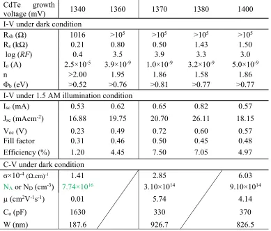
17
Table 2 summarises the results of CdS/CdTe solar cells made with CdTe layers grown in the vicinity of Vi=1370 mV. Below the Vi, the CdTe layers are p-type and therefore the devices made are p-n junctions (see Figure 6 (a)). Above the Vi, the CdTe layers are n-type and hence the device structures are n-n +Schottky barrier (see Figure 6 (b)). As shown in Table 2, the devices fabricated with n-CdTe performs better than those made with p-CdTe layers.
CdTe-based devices assuming p-CdTe in CdS/CdTe devices has been documented in the literature [27,79]. But based on recent observations, the incorporation of Cd-rich CdTe absorber layer produce high efficiencies. These effects have been independently observed and reported [80,81] and mainly attributed to the reduced defects in Cd-rich CdTe (the layers are deposited using physical deposition processes).
Table 2: Summary of device parameters obtained from I-V (both under illuminated and dark conditions) and C-V (dark condition) for simple CdS/CdTe-based solar cells grown at different growth voltages in the vicinity of Vi =1370 mV.
CdTe growth
voltage (mV) 1340 1360 1370 1380 1400
I-V under dark condition
Rsh (Ω) 1016 >105 >105 >105 >105
Rs (kΩ) 0.21 0.80 0.50 1.43 1.50
log (RF) 0.4 3.5 3.9 3.3 3.0
Io (A) 2.5×10⁻⁵ 3.9×10⁻⁹ 1.0×10⁻⁹ 3.2×10⁻⁹ 5.0×10⁻⁹
n >2.00 1.95 1.86 1.58 1.86
Φb (eV) >0.52 >0.76 >0.81 >0.77 >0.77 I-V under 1.5 AM illumination condition
Isc (mA) 0.53 0.62 0.65 0.82 0.57
Jsc (mAcm-2) 16.88 19.75 20.70 26.11 18.15
Voc (V) 0.23 0.49 0.72 0.60 0.57
Fill factor 0.31 0.46 0.50 0.45 0.48
Efficiency (%) 1.20 4.45 7.50 7.05 4.97
C-V under dark condition
σ×10-4 (Ω.cm)-1 1.41 2.85 6.03
NA or ND (cm-3) 7.74×10¹⁶ 3.10×10¹⁴ 9.10×10¹⁴
µ (cm2V-1s-1) 0.01 5.74 4.14
Co (pF) 1630 330 370
18
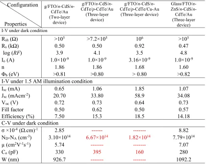
Using mainly n-CdTe absorber layers, few devices incorporating all-electrodeposited from the SHU group have been documented in the literature and summarised in Table 3.
6 Conclusion
This work describes electroplating as a robust material deposition technique with wide applications ranging from surface protection to large-area electronics and nano-technology while focusing on semiconductor deposition. The manuscript also reviews the pros and cons of electroplating technique. The effect of growth parameters such as temperature, pH, stirring rate, precursor, solvent and cathodic voltage, and post-growth heat treatments of the deposited were iterated. The capability of electroplated material to be comparable and possibly superior to semiconductor materials grown using other cash intensive techniques are Table 3: Summary of device parameters obtained from I-V (both under illuminated and dark conditions) and C-V (dark condition) for glass/FTO/n-CdS/n-CdTe/Au and glass/FTO/n-ZnS/n-CdS/n-CdTe/Au solar cells.
Configuration
Properties
g/FTO/n-CdS/n -CdTe/Au (Two-layer
device)
g/FTO/n-CdS/n -CdTe/p-CdTe/Au
(Three-layer device)
g/FTO/n-CdS/n -CdTe/p-CdTe/Cu-Au
(Three-layer device)
Glass/FTO/n -ZnS/n-CdS/n -CdTe/Au (Three-layer
device) I-V under dark condition
Rsh (Ω) >105 >7.2×10⁵ 106 >105
Rs (kΩ) 0.50 0.50 0.92 0.47
log (RF) 3.9 4.1 3.5 4.8
Io (A) 1.0×10⁻⁹ 1.0×10⁻⁹ 3.16×10⁻⁹ 1.0×10⁻⁹
n 1.86 1.86 1.68 1.60
Φb (eV) >0.81 >0.80 > 0.80 >0.82
I-V under 1.5 AM illumination condition
Isc (mA) 0.65 1.06 1.85 1.07
Jsc (mAcm-2) 20.70 33.80 58.9 34.08
Voc (V) 0.72 0.73 0.64 0.73
Fill factor 0.50 0.62 0.50 0.57
Efficiency (%) 7.50 15.3 18.5 14.18
C-V under dark condition
σ ×10-4 (Ω.cm)-1 2.85 --- --- 8.82
ND-NA (cm-3) 3.10×10¹⁴ 6.67×10¹⁴ 1.82×10¹⁴ 7.79×10¹⁴
µ (cm2V-1s-1) 5.74 --- --- 7.07
Co (pF) 330 395 160 280
19
also highlighted with experimental evidence. Electroplated materials can be applicable in large area devices such as photovoltaic solar panels and large area display panels in which intricate shapes are required. Bandgap grading, alteration of elemental composition and different conductivity type are also possible intrinsically with a change in the cathodic voltage. Other advantages such as columnar growth of nanorods which are tightly-packed and normal to the substrate could trigger many new applications in the nanotechnology area.
Acknowledgement
20 References
1. Lincot, D. Electrodeposition of semiconductors. Thin Solid Films 2005, 487, 40–48, doi:10.1016/j.tsf.2005.01.032.
2. Kröger, F. a. Cathodic Deposition and Characterization of Metallic or Semiconducting Binary Alloys or Compounds. J. Electrochem. Soc. 1978, 125, 2028, doi:10.1149/1.2131357.
3. Panicker, M. P. R. Cathodic Deposition of CdTe from Aqueous Electrolytes. J. Electrochem. Soc. 1978, 125, 566, doi:10.1149/1.2131499.
4. Danaher, W. J.; Lyons, L. E.; Morris, G. C. Some properties of thin films of chemically deposited cadmium sulphide. Sol. Energy Mater. 1985, 12, 137–148, doi:10.1016/0165-1633(85)90029-2.
5. Basol, B. M. High‐efficiency electroplated heterojunction solar cell. J. Appl. Phys. 1984, 55, 601–603, doi:10.1063/1.333073.
6. Neumann-Spallart, M.; Königstein, C. Electrodeposition of zinc telluride. Thin Solid Films 1995, 265, 33–39, doi:10.1016/0040-6090(95)06641-1.
7. Sanders, B. W.; Kitai, A. H. The electrodeposition of thin film zinc sulphide from thiosulphate solution. J. Cryst. Growth 1990, 100, 405–410, doi:10.1016/0022-0248(90)90238-G.
8. Izaki, M. Electrolyte Optimization for Cathodic Growth of Zinc Oxide Films. J. Electrochem. Soc. 1996, 143, L53, doi:10.1149/1.1836529.
9. Dharmadasa, I. M.; Burton, R. P.; Simmonds, M. Electrodeposition of CuInSe2 layers using a two-electrode system for applications in multi-layer graded bandgap solar cells. Sol. Energy Mater. Sol. Cells 2006, 90, 2191–2200, doi:10.1016/j.solmat.2006.02.028.
10. Al-Bassam, A. A. . Electrodeposition of CuInSe2 thin films and their characteristics. Phys. B Condens. Matter 1999, 266, 192–197, doi:10.1016/S0921-4526(98)01150-8. 11. Dharmadasa, I. M. Latest developments in CdTe, CuInGaSe2 and GaAs/AlGaAs thin
film PV solar cells. Curr. Appl. Phys. 2009, 9, e2–e6, doi:10.1016/j.cap.2008.12.021. 12. McHardy, J.; Ludwig, F. Electrochemistry of Semiconductors and Electronics:
Processes and Devices; Materials science and process technology series; Noyes Publications, 1992; ISBN 9780815513018.
13. Ojo, A. A.; Dharmadasa, I. M. 15.3% efficient graded bandgap solar cells fabricated using electroplated CdS and CdTe thin films. Sol. Energy 2016, 136, 10–14, doi:10.1016/j.solener.2016.06.067.
21 doi:10.3390/coatings4030380.
15. Pandey, J. Solar cell harvesting : green renewable technology of future introduction. Int. J. Adv. Res. Eng. Appl. Sci. 2015, 4, 93–103.
16. Dennison, S. Dopant and impurity effects in electrodeposited CdS/CdTe thin films for photovoltaic applications. J. Mater. Chem. 1994, 4, 41, doi:10.1039/jm9940400041. 17. Zanio, K. Semiconductors and semimetals; Academic Press: New York, 1978; Vol. 13;
ISBN 9780127521138; 0127521135.
18. Meulenkamp, E. A.; Peter, L. M. Mechanistic aspects of the electrodeposition of stoichiometric CdTe on semiconductor substrates. J. Chem. Soc. Trans. 1996, 92, 4077–4082, doi:10.1039/ft9969204077.
19. Shenouda, A. Y.; El Sayed, E. S. M. Electrodeposition, characterization and photo electrochemical properties of CdSe and CdTe. Ain Shams Eng. J. 2015, 6, 341–346, doi:10.1016/j.asej.2014.07.010.
20. Atapattu, H. Y. R.; De Silva, D. S. M.; Pathiratne, K. A. S.; Dharmadasa, I. M. Effect of stirring rate of electrolyte on properties of electrodeposited CdS layers. J. Mater. Sci. Mater. Electron. 2016, 27, 5415–5421, doi:10.1007/s10854-016-4443-3.
21. Ojo, A. A.; Salim, H. I.; Olusola, O. I.; Madugu, M. L.; Dharmadasa, I. M. Effect of thickness: a case study of electrodeposited CdS in CdS/CdTe based photovoltaic devices. J. Mater. Sci. Mater. Electron. 2017, 28, 3254–3263, doi:10.1007/s10854-016-5916-0.
22. De Alwis, A. C. S.; Atapattu, H. Y. R.; De Silva, D. S. M. Influence of the type of conducting glass substrate on the properties of electrodeposited CdS and CdTe thin films. J. Mater. Sci. Mater. Electron. 2018, 0, 0, doi:10.1007/s10854-018-9358-8. 23. Dharmadasa, I.; Madugu, M.; Olusola, O.; Echendu, O.; Fauzi, F.; Diso, D.;
Weerasinghe, A.; Druffel, T.; Dharmadasa, R.; Lavery, B.; Jasinski, J.; Krentsel, T.; Sumanasekera, G. Electroplating of CdTe Thin Films from Cadmium Sulphate Precursor and Comparison of Layers Grown by 3-Electrode and 2-Electrode Systems. Coatings 2017, 7, 17, doi:10.3390/coatings7020017.
24. Echendu, O. K.; Okeoma, K. B.; Oriaku, C. I.; Dharmadasa, I. M. Electrochemical Deposition of CdTe Semiconductor Thin Films for Solar Cell Application Using Two-Electrode and Three-Two-Electrode Configurations: A Comparative Study. Adv. Mater. Sci. Eng. 2016, 2016, 1–8, doi:10.1155/2016/3581725.
25. Sun, J.; Zhong, D. K.; Gamelin, D. R. Composite photoanodes for photoelectrochemical solar water splitting. Energy Environ. Sci. 2010, 3, 1252, doi:10.1039/c0ee00030b.
22
27. Das, S. K.; Morris, G. C. Preparation and characterisation of electrodeposited n-CdS/p-CdTe thin film solar cells. Sol. Energy Mater. Sol. Cells 1993, 28, 305–316, doi:10.1016/0927-0248(93)90118-M.
28. Daniel, L.; Michel, F.; Hubert, C. Chemical Deposition of Chalcogenide Thin Films from Solution. In Advances in Electrochemical Science and Engineering; Wiley-Blackwell, 2008; pp. 165–235 ISBN 9783527616800.
29. Ojo, A. A.; Dharmadasa, I. M. Investigation of electronic quality of electrodeposited cadmium sulphide layers from thiourea precursor for use in large area electronics. Mater. Chem. Phys. 2016, 180, 14–28, doi:10.1016/j.matchemphys.2016.05.006. 30. Salim, H. I.; Olusola, O. I.; Ojo, A. A.; Urasov, K. A.; Dergacheva, M. B.;
Dharmadasa, I. M. Electrodeposition and characterisation of CdS thin films using thiourea precursor for application in solar cells. J. Mater. Sci. Mater. Electron. 2016, 27, 6786–6799, doi:10.1007/s10854-016-4629-8.
31. Chaure, N. B.; Samantilleke, A. P.; Dharmadasa, I. M. The effects of inclusion of iodine in CdTe thin films on material properties and solar cell performance. Sol. Energy Mater. Sol. Cells 2003, 77, 303–317, doi:10.1016/S0927-0248(02)00351-3. 32. Paterson, R.; Anderson, J.; Anderson, S. S.; Lutfullah Transport in aqueous solutions
of group IIB metal salts at 298.15 K. Part 2.—Interpretation and prediction of transport in dilute solutions of cadmium iodide: an irreversible thermodynamic analysis. J. Chem. Soc. Faraday Trans. 1 Phys. Chem. Condens. Phases 1977, 73, 1773, doi:10.1039/f19777301773.
33. Paterson, R.; Devine, C. Transport in aqueous solutions of Group IIB metal salts. Part 7.—Measurement and prediction of isotopic diffusion coefficients for iodide in solutions of cadmium iodide. J. Chem. Soc. Faraday Trans. 1 Phys. Chem. Condens. Phases 1980, 76, 1052, doi:10.1039/f19807601052.
34. Dharmadasa, I. M.; Echendu, O. K.; Fauzi, F.; Abdul-Manaf, N. A.; Olusola, O. I.; Salim, H. I.; Madugu, M. L.; Ojo, A. A. Improvement of composition of CdTe thin films during heat treatment in the presence of CdCl2. J. Mater. Sci. Mater. Electron. 2017, 28, 2343–2352, doi:10.1007/s10854-016-5802-9.
35. Dharmadasa, I. M.; Echendu, O. K.; Fauzi, F.; Abdul-Manaf, N. A.; Salim, H. I.; Druffel, T.; Dharmadasa, R.; Lavery, B. Effects of CdCl2 treatment on deep levels in CdTe and their implications on thin film solar cells: a comprehensive photoluminescence study. J. Mater. Sci. Mater. Electron. 2015, 26, 4571–4583, doi:10.1007/s10854-015-3090-4.
36. Ben Nasr, T.; Kamoun, N.; Kanzari, M.; Bennaceur, R. Effect of pH on the properties of ZnS thin films grown by chemical bath deposition. Thin Solid Films 2006, 500, 4–8, doi:10.1016/j.tsf.2005.11.030.
37. Wu, W.; Eliaz, N.; Gileadi, E. The Effects of pH and Temperature on Electrodeposition of Re-Ir-Ni Coatings from Aqueous Solutions. J. Electrochem. Soc. 2014, 162, D20–D26, doi:10.1149/2.0281501jes.
23
Myung, N. V. Synthesis and characterization of cadmium telluride nanowire. Nanotechnology 2008, 19, 325711, doi:10.1088/0957-4484/19/32/325711.
39. Londhe, P. U.; Chaure, N. B. Effect of pH on electrodeposited ZnO thin films. AIP Conf. Proc. 2012, 1447, 671–672, doi:10.1063/1.4710181.
40. Kafi, F. S. B.; Jayathileka, K. M. D. C.; Wijesundera, R. P.; Siripala, W. Effect of Bath pH on Interfacial Properties of Electrodeposited n-Cu 2 O Films. Phys. status solidi 2018, 1700541, 1700541, doi:10.1002/pssb.201700541.
41. Rami, M.; Benamar, E.; Fahoume, M.; Ennaoui, A. Growth analysis of electrodeposited CdS on ITO coated glass using atomic force microscopy. Phys. Status Solidi a-Applied Res. 1999, 172, 137–147, doi:10.1002/(SICI)1521-396X(199903)172:1<137::AID-PSSA137>3.0.CO;2-V.
42. Haerifar, M.; Zandrahimi, M. Effect of current density and electrolyte pH on microstructure of Mn–Cu electroplated coatings. Appl. Surf. Sci. 2013, 284, 126–132, doi:10.1016/j.apsusc.2013.07.049.
43. Hillel, D. WATER, PROPERTIES. In Encyclopedia of Soils in the Environment; Elsevier, 2005; pp. 290–300.
44. Huang, C. A.; Chuang, C. H.; Hsu, F. Y.; Li, K. C. The Properties of ZnO Deposits Electroplated on an ITO Glass Substrate with Direct- and Pulse Currents. Int. J. Mater. Mech. Manuf. 2017, 5, 1–5, doi:10.18178/ijmmm.2017.5.1.277.
45. Basol, B. M. Electrodeposited CdTe and HgCdTe solar cells. Sol. Cells 1988, 23, 69– 88, doi:10.1016/0379-6787(88)90008-7.
46. Rastogi, A. C.; Balakrishnan, K. S. Growth, Structure and Composition of Electrodeposited CdTe Thin Films for Solar Cells. Sol. Energy Mater. Sol. Cells 1995, 36, 121–146, doi:10.1016/0927-0248(94)00167-Q.
47. Razmjoo, O.; Bahrololoom, M. E.; Najafisayar, P. The effect of current density on the composition, structure, morphology and optical properties of galvanostatically electrodeposited nanostructured cadmium telluride films. Ceram. Int. 2017, 43, 121– 127, doi:10.1016/j.ceramint.2016.09.120.
48. Donghwan Kim; Pozder, S.; Zhu, Y.; Trefny, J. U. Polycrystalline thin film CdTe solar cells fabricated by electrodeposition. In Proceedings of 1994 IEEE 1st World Conference on Photovoltaic Energy Conversion - WCPEC (A Joint Conference of PVSC, PVSEC and PSEC); IEEE, 1994; Vol. 1, pp. 334–337.
49. Ojo, A. A. Engineering of electroplated materials for multilayer next generation graded bandgap solar cells, Sheffield Hallam University, 2017.
50. Ojo, A. A.; Dharmadasa, I. M. Analysis of electrodeposited CdTe thin films grown using cadmium chloride precursor for applications in solar cells. J. Mater. Sci. Mater. Electron. 2017, 28, 14110–14120, doi:10.1007/s10854-017-7264-0.
doi:10.1016/0022-24 0728(90)85074-F.
52. Ojo, A. A.; Dharmadasa, I. M. Effect of Gallium Doping on the Characteristic Properties of Polycrystalline Cadmium Telluride Thin Film. J. Electron. Mater. 2017, 46, 5127–5135, doi:10.1007/s11664-017-5519-4.
53. Akai, T.; Kuraoka, K.; Chen, D.; Yamamoto, Y.; Shirakami, T.; Urabe, K.; Yazawa, T. Leaching Behavior of Sodium from Fine Particles of Soda-Lime-Silicate Glass in Acid Solution. J. Am. Ceram. Soc. 2005, 88, 2962–2965, doi:10.1111/j.1551-2916.2005.00524.x.
54. Madugu, M. L.; Olusola, O. I.-O.; Echendu, O. K.; Kadem, B.; Dharmadasa, I. M. Intrinsic Doping in Electrodeposited ZnS Thin Films for Application in Large-Area Optoelectronic Devices. J. Electron. Mater. 2016, 45, 2710–2717, doi:10.1007/s11664-015-4310-7.
55. Dharmadasa, I. M.; Ojo, A. A. Unravelling complex nature of CdS/CdTe based thin film solar cells. J. Mater. Sci. Mater. Electron. 2017, 28, 16598–16617, doi:10.1007/s10854-017-7615-x.
56. Chaure, N. B.; Young, J.; Samantilleke, a. P.; Dharmadasa, I. M. Electrodeposition of p-i-n type CuInSe2 multilayers for photovoltaic applications. Sol. Energy Mater. Sol. Cells 2004, 81, 125–133, doi:10.1016/j.solmat.2003.10.001.
57. Chaure, N. B.; Samantilleke, A. P.; Burton, R. P.; Young, J.; Dharmadasa, I. M. Electrodeposition of p(+), p, i, n and n(+)-type copper indium gallium diselenide for development of multilayer thin film solar cells. Thin Solid Films 2005, 472, 212–216, doi:10.1016/j.tsf.2004.07.051.
58. Delsol, T.; Samantilleke, a. P.; Chaure, N. B.; Gardiner, P. H.; Simmonds, M.; Dharmadasa, I. M. Experimental study of graded bandgap Cu(InGa)(SeS)2 thin films grown on glass/molybdenum substrates by selenization and sulphidation. Sol. Energy Mater. Sol. Cells 2004, 82, 587–599, doi:10.1016/j.solmat.2004.02.018.
59. Dharmadasa, I. M.; Chaure, N. B.; Tolan, G. J.; Samantilleke, a. P. Development of p[sup +], p, i, n, and n[sup +]-Type CuInGaSe[sub 2] Layers for Applications in Graded Bandgap Multilayer Thin-Film Solar Cells. J. Electrochem. Soc. 2007, 154, H466, doi:10.1149/1.2718401.
60. Ojo, A. A.; Dharmadasa, I. M. The Effect of Fluorine Doping on the Characteristic Behaviour of CdTe. J. Electron. Mater. 2016, 45, 5728–5738, doi:10.1007/s11664-016-4786-9.
61. Ojo, A. A.; Dharmadasa, I. M. Electrodeposition of fluorine-doped cadmium telluride for application in photovoltaic device fabrication. Mater. Res. Innov. 2015, 19, 470– 476, doi:10.1080/14328917.2015.1109215.
62. Razykov, T. M.; Ferekides, C. S.; Morel, D.; Stefanakos, E.; Ullal, H. S.; Upadhyaya, H. M. Solar photovoltaic electricity: Current status and future prospects. Prog. Sol.
Energy 1 2011, 85, 1580–1608,
25
63. Kern, W.; Schuegraf, K. K. Deposition Technologies and Applications. In Handbook of Thin Film Deposition Processes and Techniques; Elsevier, 2001; Vol. i, pp. 11–43. 64. Dharmadasa, I. M.; Samantilleke, a. P.; Young, J.; Boyle, M. H.; Bacewicz, R.;
Wolska, A. Electrodeposited p-type and n-type ZnSe layers for light emitting devices and multi-layer tandem solar cells. J. Mater. Sci. Mater. Electron. 1999, 10, 441–445, doi:10.1023/A:1008922229057.
65. Ferekides, C. S.; Marinskiy, D.; Viswanathan, V.; Tetali, B.; Palekis, V.; Selvaraj, P.; Morel, D. L. High efficiency CSS CdTe solar cells. Thin Solid Films 2000, 361–362, 520–526, doi:10.1016/S0040-6090(99)00824-X.
66. Bosio, A.; Romeo, N.; Mazzamuto, S.; Canevari, V. Polycrystalline CdTe thin films for photovoltaic applications. Prog. Cryst. Growth Charact. Mater. 2006, 52, 247– 279, doi:10.1016/j.pcrysgrow.2006.09.001.
67. Cunningham, D.; Rubcich, M.; Skinner, D. Cadmium telluride PV module manufacturing at BP Solar. Prog. Photovoltaics Res. Appl. 2002, 10, 159–168, doi:10.1002/pip.417.
68. Turner, A. K.; Woodcock, J. M.; Özsan, M. E.; Cunningham, D. W.; Johnson, D. R.; Marshall, R. J.; Mason, N. B.; Oktik, S.; Patterson, M. H.; Ransome, S. J. BP solar thin film CdTe photovoltaic technology. Sol. Energy Mater. Sol. Cells1994, 35, 263–270, doi:10.1016/0927-0248(94)90149-X.
69. Ehl, R. G.; Ihde, A. J. Faraday’s electrochemical laws and the determination of equivalent weights. J. Chem. Educ. 1954, 31, 226, doi:10.1021/ed031p226.
70. Bhattacharya, R. N.; Oh, M.-K.; Kim, Y. CIGS-based solar cells prepared from electrodeposited precursor films. Sol. Energy Mater. Sol. Cells 2012, 98, 198–202, doi:10.1016/j.solmat.2011.10.026.
71. Echendu, O. K.; Fauzi, F.; Weerasinghe, A. R.; Dharmadasa, I. M. High short-circuit current density CdTe solar cells using all-electrodeposited semiconductors. Thin Solid Films 2014, 556, 529–534, doi:10.1016/j.tsf.2014.01.071.
72. Ojo, A. A.; Dharmadasa, I. M. Analysis of the electronic properties of all-electroplated ZnS, CdS and CdTe graded bandgap photovoltaic device configuration. Sol. Energy 2017, 158, 721–727, doi:10.1016/j.solener.2017.10.042.
73. Olusola, O. I.; Madugu, M. L.; Dharmadasa, I. M. Investigating the electronic properties of multi-junction ZnS/CdS/CdTe graded bandgap solar cells. Mater. Chem. Phys. 2016, 191, 145–150, doi:10.1016/j.matchemphys.2017.01.027.
74. Abdul-Manaf, N. A.; Weerasinghe, A. R.; Echendu, O. K.; Dharmadasa, I. M. Electro-plating and characterisation of cadmium sulphide thin films using ammonium thiosulphate as the sulphur source. J. Mater. Sci. Mater. Electron. 2015, 26, 2418– 2429, doi:10.1007/s10854-015-2700-5.
26
76. Sathaye, S. D.; Sinha, A. P. B. Studies on thin films of cadmium sulphide prepared by a chemical deposition method. Thin Solid Films 1976, 37, 15–23, doi:10.1016/0040-6090(76)90531-9.
77. Abdul-Manaf, N. A.; Salim, H. I.; Madugu, M. L.; Olusola, O. I.; Dharmadasa, I. M. Electro-Plating and Characterisation of CdTe Thin Films Using CdCl2 as the Cadmium Source. Energies 2015, 8, 10883–10903, doi:10.3390/en81010883.
78. Basol, B. M. Processing high efficiency CdTe solar cells. Int. J. Sol. Energy 1992, 12, 25–35, doi:10.1080/01425919208909748.
79. Woodcock, J. M.; Turner, A. K.; Ozsan, M. E.; Summers, J. G. Thin film solar cells based on electrodeposited CdTe. In The Conference Record of the Twenty-Second IEEE Photovoltaic Specialists Conference - 1991; IEEE, 1991; pp. 842–847.
80. Reese, M. O.; Perkins, C. L.; Burst, J. M.; Farrell, S.; Barnes, T. M.; Johnston, S. W.; Kuciauskas, D.; Gessert, T. A.; Metzger, W. K. Intrinsic surface passivation of CdTe. J. Appl. Phys. 2015, 118, 155305, doi:10.1063/1.4933186.
81. Burst, J. M.; Duenow, J. N.; Albin, D. S.; Colegrove, E.; Reese, M. O.; Aguiar, J. A.; Jiang, C.-S.; Patel, M. K.; Al-Jassim, M. M.; Kuciauskas, D.; Swain, S.; Ablekim, T.; Lynn, K. G.; Metzger, W. K. CdTe solar cells with open-circuit voltage breaking the 1 V barrier. Nat. Energy 2016, 1, 16015, doi:10.1038/nenergy.2016.15.
82. Olusola, O. I.; Echendu, O. K.; Dharmadasa, I. M. Development of CdSe thin films for application in electronic devices. J. Mater. Sci. Mater. Electron. 2015, 26, 1066–1076, doi:10.1007/s10854-014-2506-x.
83. Madugu, M. L.; Bowen, L.; Echendu, O. K.; Dharmadasa, I. M. Preparation of indium selenide thin film by electrochemical technique. J. Mater. Sci. Mater. Electron. 2014, 25, 3977–3983, doi:10.1007/s10854-014-2116-7.
84. Olusola, O. I.; Madugu, M. L.; Abdul-Manaf, N. A.; Dharmadasa, I. M. Growth and characterisation of n- and p-type ZnTe thin films for applications in electronic devices. Curr. Appl. Phys. 2016, 16, 120–130, doi:10.1016/j.cap.2015.11.008.
85. Diso, D. G.; Muftah, G. E. A.; Patel, V.; Dharmadasa, I. M. Growth of CdS Layers to Develop All-Electrodeposited CdS/CdTe Thin-Film Solar Cells. J. Electrochem. Soc. 2010, 157, H647, doi:10.1149/1.3364800.
86. Samantilleke, A. P.; Boyle, M. H.; Young, J.; Dharmadasa, I. M. Electrodeposition of n-type and p-type ZnSe thin films for applications in large area optoelectronic devices. J. Mater. Sci. Mater. Electron. 1998, 9, 231–235, doi:10.1023/A:1008886410204. 87. Wellings, J. S.; Chaure, N. B.; Heavens, S. N.; Dharmadasa, I. M. Growth and
characterisation of electrodeposited ZnO thin films. Thin Solid Films 2008, 516, 3893– 3898, doi:10.1016/j.tsf.2007.07.156.