.,
.,
...-~---Achieving Uniformity in a Semiconductor Fabrication Process
Using Spatial Modeling
by
Jacqueline M. Hughes-Oliver, Jye-Chyi Lu, Joseph C. Davis and Ronald S. Gyurcsik
Institute of Statistics Mimeo Series Number 2277
August, 1995
Oepaltment
of
Slatistics library
r - - - \
! I
i'
Mimeo 112277
Achieving Uniformity in a Semiconductor Fabrication
Process Using Spatial Modeling
by
Jacqueline M. Hughes-Oliver,
Jye-Chyi Lu, Joseph C. Davis and Ronald S. Gyurcsik
Institute of Statistics Mimeo I
Seties 1/2277 ,August 1995
Name Date
IL
-"
,
'y
.
./•
Achieving Uniformity in a Semiconductor Fabrication Process
Using Spatial Modeling
Jacqueline M. Hughes-Oliver·, Jye-Chyi Lu·, Joseph C. Davis
t,
Ronald S. Gyurcsikt
An important diagnostic tool of semiconductor fabrication processes is within-wafer uniformity.
Given some required standard (for example, deposition of 1000 angstroms of polysilicon on a
blanket of silicon dioxide), the goal is to determine optimum process conditions that will achieve
this requirement uniformly across the wafer, despite possible spatial anomalies in the fabrication
process.
Processes are traditionally optimized with respect'to the process operating conditions, without
regard to spatial dependence. Nevertheless, this spatial dependence can be very important, and
is thus accounted for in our modeling of the mean, variance, and correlation of measurements
taken on a wafer. Moreover, the uniformity (or lack thereoO of the wafer surface is investigated
by the use of different metrics-based on simple averages of absolute error, or on a thin plate
spline of the error surface. These metricsar~then employed in the optimization of the process.
The techniques are illustrated through application to a Rapid Thermal Chemical Vapor Deposition
process.
KEY WORDS: Optimality criteria; Spatial correlation; Thin plate spline; Variance modeling.
• Department of Statistics. North Carolina State University, Box 8203, Raleigh NC 27695-8203.
'Dept. of Electrical&Computer Engineering, North Carolina State University, Box 7911, Raleigh, NC 27695-7911 .
• .I
1. INTRODUCTION
There have recently been numerous articles in the area of semiconductor manufacturing that attempt to integrate statistical process control and computer-aided manufacturing systems in order to improve very large scaled integrated (VLSI) circuits fabrication processes. (For example, see Mozumder, Shyamsunder and Strojwas, 1988; Sachs, Guo, Ha and Hu, 1991.) Deposition of material onto the surface of a wafer in each of the several hundred steps required to process a semiconductor chip is intimately dependent on the chamber design, the processing conditions, the wafer condition, and the stochastic error, to name a few. It is thus very difficult to guarantee the uniformity of the quality of deposition at various sites across the wafer.
In order to determine process conditions for maximizing the yield (number of high-quality chips) of a wafer, as well as for building (spatial) signatures to be able to detect possible causes of malfunctions (Chang and Spanos, 1991), it is first necessary to develop a statistical model that accurately characterizes the spatial surface. Mozumder and Loewenstein (1992) first apply the least squares method to model the polysilicon thickness on a wafer at various locations. They then regress the least squares estimates with respect to the process conditions, and optimize the spatial uniformity by minimizing the slopes of the thickness models. Guo and Sachs (1993) use a multivariate regression model to optimize and to control the spatial uniformity. They compare two different formulations of Taguchi 's (1987) signal-to-noise (SN) ratios for process optimization and conclude that modeling process responses and formulating the SN ratio for optimization is more effective than formulating the SN ratio and modeling the SN ratios for optimization.
• f
the SN ratio), however, can result in loss of information and is not flexible when the quality goal is changed, say, to look for maximum yield in a certain region. We propose to model all the observations collected on the spatial surfaces from wafers processed in a design of experiment. We are then able to link this model to whatever optimization/quality goals are desired, to find the best operating process conditions. The objective of this article is to show one example of how to formulate variance. and correlation models to characterize semiconductor deposition processes and how to utilize a thin-plate spline surface to optimize the process condition. Section 2 contains an example of a semiconductor wafer fabrication process. Section 3 contains models for the mean, variance, and correlation of the spatial responses. Section 4 contains two optimality criteria. Section 5 contains the estimated models and optimization for the wafer example. The discussion is contained in Section 6.
2. A SEMICONDUCTOR WAFER FABRICATION PROCESS
2.1 The Process
Rapid thermal processing (RTP) is quickly becoming the most novel method for semiconductor fabrication (Davis et. al., 1993). Instead of the conventional furnace where large numbers of wafers are simultaneously processed, thus leaving little room for flexibility, RTP processes a single wafer at a time. Rapid Thermal Chemical Vapor Deposition (RTCVD) is a particular RTP in which wafers are heated to facilitate the bonding of chemical vapors to the surface.
The design of the fabrication process is such that there are many possible causes for concern. The first is that the pyrometer "reads" temperature only at the center of the wafer, while it is known. that the temperature is uneven across the wafer. This is due to conduction and loss of heat due to edge effects. In fact, it is known that temperature decreases with increasing distance from the center. Even if several pyrometers were being utilized, the problems of uneven temperature would not be rectified. The pyrometer does not actually read the temperature but instead, calculates the temperature using a known functional relationship which depends on the emissivity of the surface. This surface emissivity changes as the polysilicon thickness increases, yet this is not reflected in the formula used by the pyrometer. The net effect is that as the polysilicon layer increases there is less control over the temperature of the wafer.
The response in this experiment is polysilicon thickness. As previously mentioned, this is targeted at 1000 angstroms and one would like to have uniform thickness across the wafer. In an attempt to monitor uniformity, the thickness is measured at 13 different spatial locations on the wafer. These measurement locations are displayed in Figure 1. In this diagram it can also be seen that the wafer is more or less circular, but with the bottom arc removed. The seventh measurement location, hitherto referred to as the center point, is the center of the wafer assuming the wafer forms a perfect circle.
4
o
-4
H-+----H
-4 0 4
Figure 1: Spatial Measurement Locations.
'::'
A,e 813
..
8"
..
8,e 87~ ~
•
..
i
..
..
"21 A'7...,
817 0
1il
,
8"
..
..
..
8'0..
o·
'"
A20AII600 600 1000 1200 1400
0 _ ThIckneBa
Figure 2: Experimental design, with wafer identifiers.
These edge points are also expected to display more variability. The13thmeasurement location is particularly prone to this because in addition to being far from the center point, it is closer to the edge than, say, point 9, because of the straight edge at the bottom of the wafer.
2.2 The Data
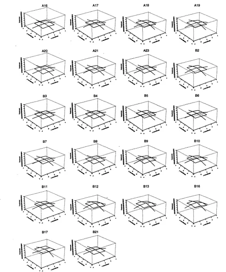
Figure 3 shows the relationship between polysilicon thickness and distance from the center point for three of the 22 wafers. Distance-from-center is clearly inversely related to polysilicon thickness. It is also clear that the variability of the thickness increases with increasing distarice from the center. In Figure 4, polysilicon thickness is plotted as a function of spatial location for each wafer. As expected, location 13 consistently has the smallest thickness while location 7 (the center point) consistently has the largest. In addition, it is clear that uniformity of polysilicon thickness within a wafer varies for different design points, as does the thickness level.
~
...
.
•
·
•
•
~
•
I
~
..
•
•
t
•
~
·
tt
~
.
,.
•
~
0 2 3 4
Distance from center
Figure 3: Polysilicon thickness versus distance from center, for 3 wafers.
3. MODELING MEAN, VARIANCE, AND CORRELATION
\
··:::::::.:::·:···.· ·;··.·.·.····::::::::'1
\ :::::::: ::.:
:·.·.·.···::::::>1
I
~
.!
l
~
.!
~
i
•
' " , !
.
" ' , . (I : 0
yo ...l .a~ " " .. .s~
A17 A18 A19
63 B4 65 66
.:.:
-:-... \ :::.:
1"
::-1\
~
!1
:~
i
...
~
J
:/~
!
~ ~ t ' ~
i
s ', .. :_ '*/
..., . .
.....
.a./
67
611
68
612
69
613
610
616
617 621
the means and variances of the response, but also for the correlation existing between the various spatial measurements. The usefulness of the mean model will be in assessing the achievement of target, as well as uniformity. The variance model is useful for measuring repeatability of the process (Mesenbrink, Lu, McKenzie and Taheri (1994); Davidian and Carroll (1987)). The correlation model affects target, uniformity, and repeatability. Itdescribes the behavioral relationship between the different spatial locations, as well as improving the estimates of the mean and variance models. Ignoring the correlation structure might result in less precise estimation of the parameters.
3.1 Notation
LetNrepresent the number of experimental runs (process operating conditions);Sthe number of spa-tiallocations;Cthe number of process variables (possibly including interaction terms);
Xl
anN xC matrix of process variables;Dthe number of spatial variables;X2 anSx Dmatrix of spatialvari-ables;Yi.theresponsefortheithrun at locations;y
=
(YI1> ... ,YIS,Y2I, ... ,Y2S, ... , YNI, ... , YNS)'the vector of responses.
3.2 The Mean Model
The most general model would allow the mean to depend on both process and spatial variables, as well as their interactions. Hence, the response is modeled as
y=X{3+€,
where
is anN S x(1
+
C+
D+
CD)matrix with components of process variables, spatial variables, and their interactions;{3is a vector of unknown parameters; and€ has a multivariate normal distribution3.3 The Variance Model
Unlike what used to be typical, it is assumed that the variance of the responses may also depend on the process conditions and the spatial location. Consequently, the variance-covariance matrixV of the responses -is modeled as
V
=
A(IN 0 R)A,whereA is an N S x N S diagonal matrix of the standard deviations ofthe responsey;logediag(A»
=
X(J(Xis defined above) so that the log of standard deviations of the response is modeled as linear combinations of process variables, spatial variables and their interactions;R is anS xScorrelation matrix of the spatial responses on a single wafer. This model assumes: 1) responses on separate wafers are independent; and 2) the spatial correlation within a wafer is the same for all experimental runs.Ifthese assumptions are not viable, thenV may be modeled asARA,whereR isNS x NS
and is the correlation matrix of the entire response vector. This latter case would contain far more parameters to be estimated.
3.4 The Correlation Model
The correlation between spatial locations s and
t
is modeled as a function of three distances: d$' thedistance between location s and the center point;dtothe distance between location
t
and the center point; andh$t, the distance between locations sandt.
The model iss=t
sid,
whereR$t is the element in the sth row and tth column of R, and61•62,and63are parameters to be
estimated.
This correlation model is constructed to satisfy several requirements based on empirical observa-tions and the mechanics of the physical RTCVD process. There are many other possible correlation models that can take into account the effects ofd. and dt . We use the correlation given above
..r
52
C\I
Gl
1ii
c:
'E
0 08
>. ~
"'t
-4 -2 0 2 4
x-coordinate
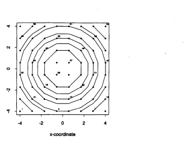
Figure 5: Grid of 64 spatial locations. Label represents the location number, and contours represent equal distance from center.
of this model, a grid of 64 spatial locations, as depicted in Figure 5, is used. Figure 5 also shows the distance contours of the locations from the center. Figures 6 and 7 show correlation contours obtained from this model for a variety of situations. The correlation between location 20 and all other locations is displayed in Figure 6. The correlation between location 55 and all other locations is displayed in Figure 7. Both figures 6 and 7 illustrate the correlation model for 6}
=
1, 62=
.25, .5,and 63
=
-.1,0,.1.First, it is expected that the correlation between two locations decreases exponentially as the distance between the locations increases. This is clearly seen in Figure 6, where, for example,
P20,28 is consistently larger thanP20,52. The effect of between-location distance on the correlation
is controlled mainly by the parameter 62 • Figures 6 and 7 show that as 62increases, the correlation
contours become closer, thereby dampening the effect of large between-location distances and exploding the effect of small distances.
delta2= 0.25 delta3= -0.1 delta2=0.5 delta3= -0.1
.48 .52 .55 .48 .52 .55 "3 .46
i
i
'Il 0
I
0~ .25 .31
~
'l' 'l'
1 1
~ ~ 1 7
..
·2..
-2x-coordlnlle x-eoordmte
delta2= 0.25 delta3= 0 della2=0.5 delta3= 0
~
~
...
.52 .48 .52 .55.46 "3 ,46
; ;
~ 0
i
0~
.®
.31~ ~
'l' 'l'
I .10 • • .1 I
~
~ ~
•
7..
·2..
·2x - c _ x-eoordinl1.
delta2= 0.25 della3=O.l della2=0.5 delta3= 0.1
.48 .52 ,55 .48
'52~
. .
.
.
.
"3 •46~
I
.37..
~
S
0~ ~
:@
,31'l' 'l'
.10 • • 3 1
~ ~
•
7..
·2..
-2x-coordina1. x-cootdJnldo
distance between them. Hence, all models assuming second order or intrinsic stationarity must be abandoned. In fact, given equal between-location distance, the correlation remains the same within radial bands from the center, but not across radial bands. For example, consider pairs of locations (19,43), (22,46), and (18,42). Although these pairs of locations share the same between-location distance (see Figure 5), since (19,43) and (22,46) fallon the same radial band, thenP19,43
=
P22,46;on the other hand, since (18,42) is on a different radial band,P18,42 =1=PI9,43' In addition, for two
locations in the same radial band, correlation decreases as distance between the locations increases, so that, for example,P19,43
>
PI9,46'The radial features of the model are controlled by 63 • When 63
=
0, there are no radial effectsand the model becomes second order stationary. This is seen in Figures 6 and 7 as concentric-circle correlation contours. When 63
>
0, pairs of locations further from the center are more highly correlated than locations closer to the center. For example, although pairs of locations (4,20) and (20,36) have the same between-locations distance,P4,20>
P20,36because the sum of the distancesof 4 and 20 to the center(d4
+
d20 ) is larger than the sum of the distances of 20 and 36 to the center(d20
+
d36). In other words, a positive value of63 implies that "edge" points behave more similarlyto each other than do "center" points. On the contrary, a negative value of 63implies that "center"
points behave more similarly than "edge" points.
Finally, in order to force the desirable positive correlations, as well as meet the requirements described above, the following constraints on the parameters are necessary:
o
<
<
{
exp(62dminexp( -263dmax ))
exp(62dminexp(-263dmin))
•
4. OPTIMALITY CRITERIA
Criteria for optimizing the process must be goal-specific. Hence, there must be penalties for: deviation from target response; lack of uniformity across the wafer; and large variability of response. The criteria described below address all these aspects with increasing complexity. The first criterion takes the "optimize on summary statistics" approach, while the second criterion takes the "optimize on the entire surface" approach. As a result of having closed form expressions for the criteria, they may be easily implemented using common minimization routines. Of course, the efficiencies of these routines will depend on your particular application. We hasten to add that the literature on optimality criteria is very large, and so no claim is made of this being an exhaustive presentation.
For ease of presentation, slightly differing notation than that used in Section 3 is introduced:
s
=
# spatial measurement locations on a wafer; y=
vector of responses on a single wafer;m=
expected value ofy; v
=
vector of standard deviations ofy; C=
correlation matrix ofy; T=
target response.
The first criterion attacks the problem with brute force: minimize the average standard deviation, subject to the average absolute error being within tolerance. By focusing on minimization of the average standard deviation, much attention is given to the issue of repeatability. Low standard deviation indicates that repeating the experiment using the same process conditions will result in very similar responses. The constraint that absolute error is within a given tolerance addresses the issue of meeting target. The averaging, which is done across spatial measurement locations, attempts to address uniformity by looking at the average behavior rather than the individual or worst-case behavior. In symbols, the criterion is
Minimize
1 ,
-Iv s
subject to
1
-I'abs(m - T
*
1)<
tolerance.s
•
I
There are, however, several disadvantages with this approach. One such disadvantage is that a value for tolerance needs to be provided. Another disadvantage is that there is no immediate measure of within-wafer uniformity. Also, the averaging done across measurement sites causes loss of uniformity information, as the mean may be unduly influenced by one or two stray values of the limited number of measurement locations available. Yet another disadvantage is the inability to assign unequal weights to the activities of making the process repeatable and achieving target. Finally, in this approach the correlation structure is ignored.
The second criterion is based on first obtaining the error surface of the wafer-the difference between the responses and the target. This surface will have both positive and negative values, so we choose to look at the squared error surface. The integral of this squared error surface can serve as a measure of within-wafer uniformity, with an ideal value of zero. This integral also measures the ability to meet target, since the difference is with respect to target. As a function of the responses, this integral metric is itself a random quantity with an associated distribution, expected value, and variance. The expected value of the integral metric is chosen to represent this distribution, and criterion 2 minimizes this value. The criterion is
Minimize
trace(Adiag(v)Cdiag(v)A')
+
(m -
T*1)'A' A(m - T *1), (I)where the matrixA is described below. Repeatability issues are automatically considered because the variance and correlation of the responses are introduced in the first component of equation (1).
The matrixA is determined by applying an interpolating natural thin plate spline to thes spatial
responses in y in order to obtain the error surface on the wafer. The typical representation of a . natural thin plate spline is
n 3
get)
=
2:
c5i7](lIt -ti
II)+
2:
aj4>j(t),
i=1 j=1
where the spatial locations (x- and y-coordinates) are represented by t; there are n data points at locations
tl, ... ,
in;
7](-) is a function of distance between locations;4>1
(t)=
1, 4>2(t)=
x-coordinate of
t, 4>3(t)
=
y-coordinate oft;
Danda are solutions to a system of equations involvingthe data
z.
It turns out, however, that this equation is a linear combination of the data, so that we may use the modified representationget)
=
u'z.
(For more detail, see Green and Silverman, 1994.) So to represent the spline atN selected spatial locations, it is possible to use the matrix representationAz,whereA hasncolumns and N rows. Moreover, the sum of the columns ofA is the vector of 1'so
The error surface for criterion 2 may then be written as A(y - T
*
1),where the matrix A is obtained from a sufficiently fine grid of locations on the wafer. Numerical integration of the squared error surface is more tractable that exact integration and, provided a fine enough grid of locations is used to obtainA,may be approximated ask*
(y - T*
1)'A' A(y - T*
1),wherekis a constant representing the area of the grid points relative to the area of the wafer. Hence, ignoring the constant5. APPLICATION TO RTCVD PROCESS
5.1 Model Fitting
For the wafer fabrication process described in Section 2, the matrixX is such that the mean and
Maximum likelihood estimation is used to obtain the estimates of{3,(JandD. The estimated mean model is
984.5 - 260.20x+ 326.6ti+58.80x2-42.7ti2- 97.60x*ti+0.96d-l1.6d2+ 14.1d*ox- 8.6d*ti,
where ox represents the coded oxide thickness [ -1 represents 458 angstroms, 1 represents 1498 angstroms ], ti represents the coded deposition time [-1 represents 18 seconds, 1 represents 52 seconds], and d represents the distance of the spatial location from the center point. The estimated log(standard deviation) model is
2.73 - 0.480x + 0.08d + 0.07d2- 0.02d*ox.
The estimated correlation model is
,
i >
.
···T···....
(ox,b)=(O,O)
···_····_··-r···.
(OX,b)=(O,O)
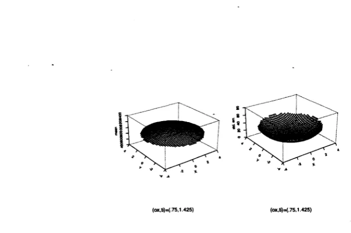
Figure 8: Estimated mean and standard deviation surfaces. Process conditions: ox=O, ti=O.
and likelihood ratio tests indicate the statistical significance of all three parameters(01 , 02, 03)of this model.
Figures8-10graph the estimated mean and standard deviation surfaces for selected settings of process conditions. Figure 8 shows that when oxide thickness and deposition time are at their center values (with respect to the experimental design) the mean surface is fairly uniform, but off target. At the same time the measurement locations closer to the edge show far more variability than those close to the center of the wafer. On the other hand, Figures 9 and 10 show both good achievement of target and repeatability.
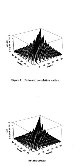
To illustrate the correlation model, the finer grid of 64 spatial locations (not the 13 actual measurement locations) used in Section 3 is again used here (see Figure 5). Figure11contains the graph of the estimated correlation between these 64 locations. In order to demonstrate the effect of the "non-stationary" component of the correlation model, where distance to center point affects the correlation, Figure 12 shows the same correlation model without this piece.
5.2 ProcessOptimization
,
•
... .···r···.......••.... ....:>!
...: ..
..•.•....
:l···~··::·
..:·;
.
~;
(ox,b)-(.9,1.5) (ox,b)z(.9,1.5)
Figure 9: Estimated mean and standard deviation surfaces. Process conditions: ox=.9, ti=1.5 .
....! ... ...
1~~.:J
.
•
(ox,b)=(.75,1.425) (ox,b)=(.75,1.425)
4
f
CD
o
-=~
t:~80
"!
o o
Figure 11: Estimated correlation surface.
«!
o
CD
Ii 0
8"':o
N
o
o
,
(dell.del2)=(.61596.0)4
I
... ..."1....
···..···:::>1
...1' ..
. .
n .
,
Figure 13: Optimality criterion 1
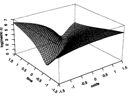
certain tolerance) while minimizing the variance of the thickness and achieving uniformity across the wafer. Based on the estimated models given in the previous section, criteria 1 and 2 are applied to this RTCVD process. A tolerance value of 60 angstroms (6% of the target) is used for criterion 1. Figures 13 and 14 show the logarithm of the metrics of the criteria over a grid of (ox, ti) settings. Figure 13 shows the average standard deviations, which is a plane since deposition time is not a part of the standard deviation model, and the average absolute error, which has a trough-like shape. Figure 14 for metric 2 has the same shape of the average absolute error surface, showing this as the dominant determinant of process conditions.
f (
... .... '.
o
.,
...~' .
...
.\
~ ..
Figure 14: Optimality criterion 2
Table 1. Optimal process conditions for the two criteria. Optimum Value of Metric for
Criterion (ox,ti) Criterion 1 (Constraint 1) Criterion 2 1 (0.9,1.350) 23.20393 58.60250 3578308 (0.9,1.425) 23.20393 57.48159 3191891 (0.9,1.500) 23.20393 56.47161 2899806 2 (0.75,1.425) 25.17286 51.31676 2321446
criteria.
6. DISCUSSION
t
believed that the variability on an experimental unit is bowl-shaped.
Optimality criteria have also been presented and their use illustrated on a real problem. The metric involved in one of these criteria may also be used as an indicator of within-wafer uniformity, even in the absence of desires to optimize a process.
REFERENCES
Chang, N. H. and Spanos, C. J. (1991). Continuous equipment diagnosis using evidence integration: An LPCVD application. IEEE Trans. on Semiconductor Manufacturing, 4(1), 43-51. Davis, J. C., Gyurcsik, R. S., and Lu, J. C. (1993). Application of semi-empirical model building
to the RTCVD of polysilicon. Statistics in the semiconductor industry - Case studies of
process/equipment characterization, vol. 2, Chapter 4,202-214. SEMAlECH.
,;..
Davidian, M. and Carroll, R.J. (1987). Variance function estimation. Journal of the American
Statistical Association, 82, 1079-1091.
Green, P. J. and Silverman, B. W. (1994). Nonparametric Regression and Generalized Linear
Models. Chapman& Hall.
Guo, R. and Sachs, E. (1993). Modeling, optimization and control of spatial uniformity in manu-facturing processes. IEEE Trans. on Semiconductor Manumanu-facturing, 6(1), 41-57.
Mesenbrink, P., Lu,J.C., McKenzie, R., and Taheri,J.(1994). Characterization and optimization of a wave soldering process. Journal ofthe American Statistical Association, 89, 1209-1217. Mozumder, P. K. and Loewenstein, L. M. (1992). Method for semiconductor process optimization using functional representation of spatial variations and selectivity. IEEE Trans. on
Compo-nents, Hybrids, and Manufacturing Technology, 15(3), 311-316.
Mozumder, P. K., Shyamsundar, C. R., and Strojwas, A.J. (1988). Statistical control of VLSI fabrication processes: A framework. IEEE Trans. on Semiconductor Manufacturing, 1(2), 62-71.
Sachs, E., Guo, R., Ha, S., and Hu,A.(1991). Process control system for VLSI fabrication. IEEE
Trans. on Semiconductor Manufacturing, 4(2), 134-144.
Taguchi, G. (Technical editor for the English Edition: Don Clausing) (1987). System of