Hans Hallen).
This work invents and develops a new technique for electrical, electro-optical, and
topographical characterization at the nanoscale. Split-tip scanning capacitance microscopy
(SSCM) offers advantages over other scanning probe methods. The dependence of the
measurements on sample characteristics is reduced, and analysis is simplified by having both
electrodes secured to the probe. This feature allows non-conducting, as well as conducting
surfaces to be imaged without loss of optical or capacitance resolution. SSCM allows
surface measurements without destroying the sample of interest and does not require special
surface preparation. To develop this new technique, the project focused on the following:
• shear-force feedback as an accurate tip-sample distance controller • imaging techniques for irregular sample surfaces
• development of computational model for simulating split-tip measurements • split-tip integration into a conventional near-field scanning optical microscope • contrast modeling for surface structures
• tip-sample approach capacitance measurements as a stringent test of SSCM.
We show that a non-linear tip sample interaction dominates the shear force feedback
signal evidenced by a change in the resonance frequency as the tip approaches the sample.
Shear force feedback relies on a decrease in the signal amplitude at the operating frequency.
We present data and a numerical model describing the time response and how this nonlinear
distribution of pigment quantified by the peak in the histogram of optical signal versus
separation at the nano- to micron scale illuminates the length-scale of failure in paint
samples. We compare a high quality paint sample with one that fails a standard quality
control test based upon visual inspection. Features such as pigment clumping and pigment
density fluctuations are simultaneously analyzed. Individual pigment particles are observed
near the polymer surface of both samples.
We develop a split-tip model that yields the capacitance across the split-tip and also
gives related insights into the origins of the features and behaviors via related calculated
values such as charge and energy density. We elucidate these properties using computational
finite element methods for several simple examples. The model yields insights into
resolution and field enhancement effects near the probe edges.
We describe the fabrication of the novel split-tip optical nanoprobe that is used in the
SSCM setup. The split-tip nanoprobe can be used to both orient molecules with a strong,
localized electric field and deposit them, and to measure capacitance, energy density, and
charge. The process for mounting this probe for integration in SSCM is also described; this
mounting process allows reliable contact to be made to each probe electrode while meeting
the stringent requirements for shear-force feedback with the probe. Data is collected from
the split-tip with the use of a capacitance bridge circuit integrated into the scanning probe
setup.
Lastly experimental measurements with the SSCM tie the above results together.
Split-tip capacitance measurements with respect to tip-sample distance provide a critical test
between the probe electrodes and how it varies with respect to distance from the sample
surface. We present approach capacitance measurements made on a sample comprised of
aluminum structures deposited on a silica substrate grating. The experimental data is
compared with the finite element model to gain more insights on the localized edge effects
Split-tip Scanning Capacitance Microscopy (SSCM): Special Techniques in Surface Characterization and Measurements
by
Beverly Andrew Clark, III
A dissertation submitted to the Graduate Faculty of North Carolina State University
in partial fulfillment of the requirements for the Degree of
Doctor of Philosophy
Physics
Raleigh, North Carolina
2009
APPROVED BY:
Dr. H.D. Hallen Dr. C. Roland
Chair of Advisory Committee
DEDICATION
I dedicate this dissertation to my mother, Althera Clark.
A woman who taught me education was important through example.
A woman who taught me to be dedicated and steadfast even in the bleakest hour.
A woman of valor and character.
A woman with extreme devotion to education.
A woman who sacrificed so that I would succeed.
A woman I love with all my heart.
In loving memory of:
Booker & Gladys Callands,
Beatrice Clark,
and
BIOGRAPHY
In 1976, Beverly was born in rural Virginia to Althera and Beverly Clark, Jr. and
grew up in a modest home located in Java. At an early age, Beverly found an interest in
science and music, and both have been constants throughout his life. He was educated in
Pittsylvania County Public Schools graduating from Chatham High School in 1994. Upon
completion of high school, Beverly attended Emory & Henry College (E&H) and majored in
Physics. During his time at E&H, Beverly was involved in numerous on and off campus
activities. Along with studying physics, Beverly was a four-year letterman on the E&H
football team, a resident advisor, and bassist for the college gospel choir (Spiritual
Harmony), co-founded by Beverly and numerous other students. After graduating in 1999
with a Bachelor of Science, Beverly taught English as a second language in Lins, Brasil
before entering the graduate program at North Carolina State University (NCSU).
At NCSU, Beverly immediately started working for Hans Hallen in the Near-Field
Optics Lab quickly learning the basics of scanning probe microscopy. During his graduate
career, Beverly was a General Electric Fellow as well as a Graduate Assistant in Areas of
National Need (GAANN) Fellow. In 2003, Beverly received a Masters of Science from
NCSU and continued with his graduate studies. From 2003-2004 he also served as president
of the NCSU Association for the Concerns of African American Graduate Students
saxophone for numerous local and national recording artists such as Chrisette Michele, Kevin
Hill (K-Hill), Tyrand, and many others.
On June 10, 2009 Beverly successfully defended his Doctorate of Philosophy in
Physics, completing his graduate studies. Science and music have remained constants in
ACKNOWLEDGEMENTS
I would like to acknowledge some of the many people who have helped and supported me
during my graduate studies.
I would like to thank my research advisor Dr. Hans Hallen. Over the years, you have
helped me more than you will ever know. Since 1998 (summer REU Program), you have
been instrumental in my development as a scientist, and I will always be grateful for your
assistance and guidance.
To my advisory committee (Dr. H. Hallen, Dr. C. Roland, Dr. M. Paesler, and Dr. W.
Alexander), I would like to thank you for your insight on all aspects of my academic work
and research. I extend a special thanks to Dr. Paesler for his continuous guidance and
encouragement throughout my graduate studies.
Special thanks to the National Science Foundation for support through grants
DMR-9975543 and DMII-0210058, the Research Corporation through grant CC5342, and the U.S.
Department of Education Graduate Assistance in Areas of National Need (GAANN)
Fellowship Program (P200A000854). Thanks Gamil Guirgis for providing the paint samples
imaged in Chapter 3.
Thanks to the members of the NCSU Near-field Optics Group especially Jeremy
Peters, Trey Walker, and Ryan Neely for the enjoyable, thought-provoking conversations and
To Dr. Mike Taylor and Dr. Christopher Chadwick: it has been an eventful 10 years
with numerous ups and downs. It has been filled with lab relocations, water leaks, and flash
floods, but we all made it through thanks to the support we have shown one another. We
have definitely been banded together in brotherhood through this experience, and I will
always cherish the friendships we have formed.
Lastly, I would like to thank Angela Combs Richardson for being a source of support
and encouragement during the completion of my graduate work. I truly appreciate all the
kind words and every act of support you have shown me. I love you and thank God for your
TABLE OF CONTENTS
LIST OF FIGURES... ix
1. Introduction... 1
1.1 Bibliography... 5
2. Shear-force Feedback... 7
2.1 Nonlinear Tip-Sample Interaction... 7
2.2 Data Analysis... 16
2.3 Bibliography... 17
3. Imaging Techniques of Irregular Surfaces... 19
3.1 Introductory NSOM... 19
3.2 Imaging Methods... 20
3.3 Imaging Results... 21
3.4 Single Pigment Particle Imaging... 25
3.5 Data Analysis... 27
3.6 Bibliography... 29
4. Novel Split-Tip Proximal Probe for SSCM and Fabrication of Nanometer-Textured, In-Plane Oriented Polymer Films... 30
4.1 Introduction... 30
4.2 Probe Fabrication Methods... 33
4.2.1 Probe Design Criteria... 33
4.2.2 Probe Fabrication... 34
4.2.3 Probe Mounting... 37
4.2.4 Probe Usage... 39
4.3 Results & Discussion... 40
4.4 Data Analysis... 46
4.5 Bibliography... 48
5. Split-Tip Scanning Capacitance Microscopy (SSCM): A Finite Element Model... 50
5.1 Introductory Modeling... 50
5.2 Model Methods... 52
5.2.1 Lateral Capacitance Scans... 54
5.2.2 Approach Capacitance Scans... 56
5.2.3 Dopant Density Scans... 58
5.3 Model Results and Discussion... 59
5.4 Data Analysis... 63
5.5 Bibliography... 65
6. Split-Tip Scanning Capacitance Microscopy (SSCM)... 66
6.1 Introductory Split-Tip Scanning Capacitance... 66
6.2 SSCM Split-tip Holder... 67
6.4 Sample Grating... 70
6.5 Measurement Sequence... 71
6.6 SSCM Experimental Results... 72
6.7 SSCM Data Analysis... 82
6.8 Bibliography... 84
LIST OF FIGURES
Figure 2. 1: (a) Typical resonance curves obtained with the tuning fork method of oscillation amplitude measurement at various tip-sample separations (solid lines). (b) Resonance curves with different degrees of tapping obtained by a numerical solution of the nonlinear
differential equation... 8
Figure 2. 2: (a) The numerical calculation of the time response for the feedback signal to drop to 1/e for a variety of driving frequencies for two situations: turning the tapping off and turning the tapping on. This time response is overlaid with the resonance curve for reference. (b) The experimental time response for the probe to find the surface with optimized gain given an 8msec-ramped trapezoidal step of height 30 nm... 11
Figure 2. 3: The feedback response to an impulse of 40 nm on the z-piezo for a variety of driving frequencies on either side of the resonant frequency with constant gain. The black lines are the outward motion. The grey lines are the inward motion. The resonance curve is overlaid for reference... 13
Figure 2. 4: Experimental resonance curves showing the undamped resonance, a resonance at 35% of the free resonance and a clamped resonance curve. The peak of the clamped resonance is only 2% of the undamped resonance peak, and the frequency shift is ~400Hz. 14
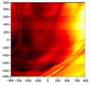
Figure 3. 1: This is a topographic scan of the reference sample (1905nm x 1905nm). The axes are in nanometers. The overall z distance range is 1138nm. The middle region of the image represents one plateau at a vertical position near 228nm. The upper middle portion of the image is 187nm above the middle plateau, and the bottom right where polymer ridging is observed is 663nm below the middle plateau. ... 23
Figure 3. 2: This is an optical scan of the reference sample (1905nm x 1905nm). The optical range was measured in arbitrary units. The horizontal axis is in nanometers. There is an overall optical range of 0.051a.u. In the upper left and lower right portions of the image, polymer ridging is observed. This is consistent with Figure 3.1, which was taken over the same scan range. ... 24
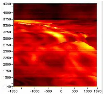
Figure 3. 3: This is an optical scan of the low quality sample (3175nm x 3175nm). The horizontal axis is in nanometers. There is an overall optical range of 0.27a.u. The scan shows pigment particle clumping in a non-uniform manner. Although the arrangement is non-uniform, it is still possible to identify pigment particles (see Figure 3.5)... 25
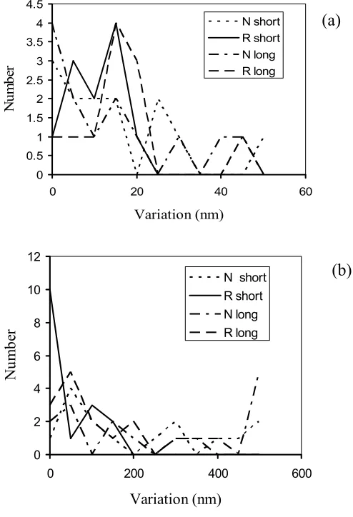
Figure 3. 4: (a) is a histogram of the optical variation and (b) a histogram of the
topographical variation. In analyzing the percent variation, it is possible to distinguish between the reference and low quality sample. ... 26
corresponding data points in the forward and backward data that reflect the same pigment particles... 27
Figure 4. 1: The split-tip probe has electrodes on the left and right sides, and the aperture located at the bottom... 32
Figure 4. 2: Figure shows a schematic of the split-tip near the sample as molecules are deposited. ... 33
Figure 4. 3: SEM image of a larger-aperture tapered fiber fabricated by the heat-and-pull method. Note the flat cleaved end that is formed when this fabrication scheme is used, as opposed to the sharp point of etched fibers. ... 35
Figure 4. 4: The end of a split-tip fabrication with the optimal fabrication procedures... 37
Figure 4. 5: A photograph of the tip holder; a piece of glass shaped to hold the tip on a tuning fork (upper right portion), the Teflon holder on the upper left keeps the gold wires positioned for contact with the fiber. The fiber can be seen passing through the groove in the Teflon where it contacts the wires, and on to the tuning fork (partially hidden)... 38
Figure 4. 6: (a) shows split-tip probe fabricated with certain imperfections, such as voids in the coating. (b) shows cracking and peeling which presents a significant problem. (c) shows tensile stress. ... 41
Figure 4. 7: Figure shows a detailed view of the separation between the split-tip electrodes. The split is not completely void, containing small grains of material... 45
Figure 5. 1: Image of the split-tip probe positioned over a nanorod and substrate. The split is perpendicular to the rod and substrate... 54
Figure 5. 2: Split tip rotated about y axis by 90 degrees. ... 55
Figure 5. 3: Split-tip probe is located 10nm above the substrate surface. Aluminum and silica substrates were scanned varying the vertical distance in y. ... 57
Figure 5. 4: Boundary conditions slightly modified for dopant density measurements. Substrate has conductivity varied and capacitance measurements made. ... 59
Figure 5. 5: This is a plot of the lateral capacitance between the split-tip probe electrodes with the split parallel to the nanorod and substrate... 60
Figure 5. 6: This is a plot of the lateral capacitance between the split-tip probe electrodes with the split perpendicular to the nanorod and substrate... 61
Figure 5. 7: Plot of the capacitance between the electrodes. The horizontal axis shows vertical absolute values labeled d. ... 62
Figure 5. 8: Graph shows the capacitances calculated for n-type materials with different conductivities. ... 63
Figure 6. 1: Image of Standard NSOM setup with PMT (top left) used for optical data collection. The probe and tuning fork are mounted to the glass tip holder, with the sample mounted to the piezo electric tube for fine adjustment (top center). Course adjustment is achieved with a stepper motor (right middle). ... 68
Figure 6. 3: This is a plot of the experimental data taken from the aluminum grating
structure. There were 2000 capacitance points read in over a 750nm z-range. ... 73
Figure 6. 4: Plot of approach capacitance versus z from the aluminum grating structure. The 0-550nm range spans over regions (a) and (b) from Figure 6.3. ... 75
Figure 6. 5: This is a plot of the experimental data taken from the aluminum grating structure (shown in Figure 6.3) with the sample surface correctly shifted to z = 173nm and the drift from the capacitance bridge circuit removed. ... 76
Figure 6. 6: Plot shows various aluminum capacitance profiles taken from Figure 6.5. Plot compares capacitance profiles for two different data sets taken near the sample surface. The vertical axis shows Capacitance (pF) and z (nm), shown on the horizontal axis, give the distance near the sample surface... 77
Figure 6. 7: This is a plot of the experimental data taken from the silica grating structure. There were 2000 capacitance points read in over a 750nm z range. ... 78
Figure 6. 8: Plot of the silica approach capacitance versus z values taken from region (b) of Figure 6.7. ... 79
Figure 6. 9: Plot shows various silica capacitance data sets taken near the surface. The capacitance is plotted as a function of the z values to more accurately compare the
capacitance profiles near the sample surface. ... 80
Figure 6. 10: Plots compare various experimental capacitance profiles from aluminum and silica sample scans to the Femlab model values. The green line indicates the range of data comparable to the Femlab model, which is the first 25nm of capacitance values... 81
Chapter 1
1. Introduction
This work invents and develops a new technique for electrical, electro-optical, and
topographical characterization at the nanoscale. Split-tip scanning capacitance microscopy
(SSCM) offers some advantages over other scanning probe methods. The dependence of the
measurements on sample characteristics is reduced, and the analysis is simplified by having
both electrodes secured to the probe. SSCM differs from the related, single tip AFM-based
versions by having both electrodes secured to the probe 1,2,3. This reduces the dependence of
the measurements on sample characteristics and simplifies the analysis 4. SSCM allows the
imaging of simultaneous topographic, optical, and electronic structures 5,6. This feature
allows non-conducting, as well as conducting surfaces to be imaged without loss of optical
measurements in a non-contact manner. Unlike conventional scanning capacitance methods,
SSCM allows measurements without destroying the sample of interest. To develop this new
technique, the project focused on the following concepts:
• shear-force feedback as an accurate tip-sample distance controller 8,9,10 • imaging techniques for irregular sample surfaces 11
• computational models or simulating split-tip measurements
• split-tip integration into a conventional near-field scanning optical microscope • contrast modeling for simple surface structures
• tip-sample approach capacitance measurements as a stringent test of SSCM.
The project first focused on improving the shear-force feedback process for
high-resolution imaging. To improve the shear force feedback of the experimental setup, we
exploit the non-linear tip sample interaction which relies on a decrease in the amplitude of
the signal at the resonance frequency. This decrease occurs due to an increase in the quality
factor (Q) and a high frequency shift in the resonance. The resonance shift is also a result of
the nonlinear tip-sample interaction. The change in Q is slow, while the frequency shift is
fast 8, 9, 10, 12. This process has proven effective in the SSCM experimental setup and has
improved data collection.
Next, the project shifted to imaging techniques and statistical analysis. Paint samples,
with irregular surfaces, were resolved revealing mesoscopic distributions of pigment and
the best distribution is peaked on a mesoscopic scale. Single pigment particle imaging
provided insight on the optical resolution, since the pigment particles were on the order of the
imaging resolution. This project provided needed insight into imaging rough, irregular
surfaces.
After improvement on feedback and imaging techniques, the focus shifted to
developing a split-tip holder, fitting the split-tip probe into the V-groove holder that provided
stability and reproducibility. Simultaneously we developed a model to provide insights on
capacitance values found from finite element measurements, and collecting capacitance
measurements from the SSCM experimental setup.
Novel fabrication schemes are required to deposit nanoscale materials that contain
molecules oriented in the plane of the surface 13. We present the fabrication of a novel
split-tip optical nanoprobe that can be used to both orient the molecules with a strong, localized
electric field and deposit them with nanoscale resolution. Ultraviolet light injected through
the probe into the region of aligned molecules completes the deposition. The production of
the split-tip probe is significantly different than that of the related near-field scanning optical
microscope (NSOM) probe 14, 15, due to film stress issues. Mounting of the probe to insure
reliable electrical contacts is also described.
Lastly, the capacitance properties are elucidated using computational (finite element)
methods 16, 17. The computational model also yields insight into resolution and field
applied in developing a more complicated, but still symmetrical model. The results indicate
that local measurements of doping levels in semiconductors is possible. Values obtained
from the finite element model are compared to SSCM experimental values. The more
advanced model of the split-tip probe yields results of capacitance and other related values
such as energy density and charge. Approach capacitance measurements from the SSCM
experimental setup are presented and discussed. From the on (aluminum) and off (silica)
grating capacitance measurements, properties like charge, energy density, and capacitance
are distinguished.
1.1 Bibliography
1. Stefan Lanyi and Miloslav Hruskovic, J. Phys. D Appl. Phys. 36, 598 (2003).
2. H.D. Hallen, A.H. La Rosa and C.L. Jahncke, Phys. Stat. Sol. (a) 152, 257(1995).
3. A.H. La Rosa, B.I. Yakobson, and H.D. Hallen, Mater. Res. Soc. Symp. Proc. 406, 189 (1995).
4. H.E. Ruda and A. Shik, Phys. Rev. Lett. B 67, 235309 (2003).
5. K. Karrai and R. Grober, Proc. SPIE 2535, 69 (1995).
6. R. Brunner, A. Bietsch, O. Hollricher, and O. Marti, Rev. Sci. Instrum. 68, 1769 (1997).
7. E. Betzig, P. Finn, and J.S. Weiner, Appl. Phys. Lett. 60, 2484 (1992).
8. X.S. Xie and R.C. Dunn, Science 265, 361 (1994).
9. E.J. Ayers, H.D. Hallen, and C.L. Jahncke, Phys. Rev. Lett. 85, 4180 (2000).
10. S.H. Huerth, M.P. Taylor, H.D. Hallen, and B.H. Moeckley, Appl. Phys. Lett. 77,
2127 (2000).
11. B. Clark III, G. Gurguis, H.D. Hallen, J. Vac. Sci. Technol. B 25, 54 (2007).
12. C.L. Jahncke, S.H. Heurth, B. Clark III, and H.D. Hallen, Appl. Phys. Lett. 81, 4055 (2002).
13. M.P. Taylor and H.D. Hallen, “Fabrication of Nanoscale Polymer Structures with In-Plane Molecular Orientation”. Manuscript.
14. C.L. Jahncke and H.D. Hallen, J. Appl. Phys. Lett. 93, 1274 (2003).
15. E. Betzig and J. Trautman, Science 257, 189 (1992).
17. P. Pomorski, C. Roland, H. Guo, and J. Wang, Phys. Rev. Lett. B 67, 161404(R)
Chapter 2
2. Shear-force Feedback
2.1 Nonlinear Tip-Sample Interaction
Distance regulation in near-field optical microscopy (NSOM) makes use of the force
interaction between the probe and sample. There are several experiments in which accurate
distance control is essential: fluorescence lifetime, gradient field Raman, SSCM and
electromigration 1, 2, 3, 4. Understanding the dynamics of the probe interaction and the
mechanism behind the distance control helps to optimize distance regulation and evaluate its
accuracy. We find that a nonlinear interaction such as a tapping force is required to
accurately describe the resonance behavior of the probe both in and out of feedback (near and
far from the sample). Furthermore, our novel study of the system dynamics shows that the
in our measurements. Finally, we present strong evidence indicating that the probe is tapping
on surface adlayers prior to tapping on the surface itself as the probe approaches the sample,
and we comment on the suitability of shear-force feedback for accurate distance control.
0.2
0.4
0.6
0.8
1
1.2
1.4
1.6
35.2
35.25
35.3
35.35
35.88
35.9
35.92
35.94
35.96
35.98
36
Free
86%
75%
63%
56%
Free
85%
75%
65%
50%
Normalized Amplitude
frequency (kHz) experiment
frequency (kHz) model
(b)
(a)
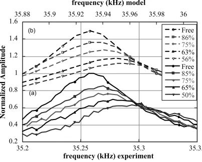
Figure 2. 1: (a) Typical resonance curves obtained with the tuning fork method of oscillation amplitude measurement at various tip-sample separations (solid lines). (b) Resonance curves with different degrees of tapping obtained by a numerical solution of the nonlinear differential equation.
Shear force feedback using a tuning fork oscillator is one of the most widely used
techniques for controlling tip sample separation with NSOM 5. It relies on voltage
sample distance. The oscillation amplitude decreases when the probe is close to the surface
due to an increase in damping and a shift in the resonance frequency. A variety of
mechanisms and combinations of mechanisms are proposed to be responsible for the
interaction between the probe and the sample such as friction 6, tapping (or knocking)7,8,9,
distance dependent probe bending 10, damping layer 10-14, and coulomb fields 15. In this
dissertation we show evidence of a nonlinear tip-sample interaction. Of these mechanisms,
only tapping and probe bending have a nonlinear response. Figure 2.1(a) shows the
resonance curve far from the surface and its evolution as the probe is moved closer and closer
to the surface. The resonance frequency shift seen implies that a nonlinear mechanism is
active. The obvious nonlinear interaction is tapping.
To model this tapping interaction, we use a simple truncated driven harmonic
oscillator used by others to model NSOM 7 and atomic force microscope 16 probe-sample
interactions. In this model, the tapping force is included in the addition of a strong force
when the lateral position of the tip exceeds a critical value, xc. The equation that describes
such a system with effective mass meff driven by a force Fdrive is
Fdrive/meff = F0cos(ωdt)/meff = x¨ + 2β0x• + ω0 2
x + H(x-xc)[ ω1 2
(x-xc) + 2β1x•] , (1)
where ωd is the radial tip oscillation driving frequency, β0 and β1 refer to damping and ω0
and ω1 the resonance frequencies of the fork/fiber oscillator and fiber/adlayer system,
respectively, and H is the step function. We find ω0 and β0 from the free resonance curve.
free resonance curve (H=0) and a shifted, damped resonance curve we determine ω1 and β1.
We comment in more detail on the significance of the values of these two parameters for the
physics of the tip-sample interaction later in the paper.
The parameter F0/meff is used to normalize the equations so that the amplitude of x is
1 with no tapping (H=0). Numerical solutions to the model for various values of xc give
resonance curves as a function of the fraction of the undamped resonance peak (set-point)
that are consistent with the resonance curves we find in our experiments (see Figure 2.1).
Note that in both the numerical analysis and in the experiment, the damped resonance curve
crosses over the free resonance curve on the high frequency side resulting in driving
frequencies unavailable for normal feedback operation without switching the polarity of the
feedback response.
We study the dynamics of the probe sample interaction by observing the calculated
oscillation x(t) as we add or remove the step function terms from the model. When we add
the step function, we refer to the system as tapping on, and when we remove the step
function, we refer to the system as tapping off. This is analogous to the probe being moved
from a position out of feedback to a position close to the sample for the tapping on and vice
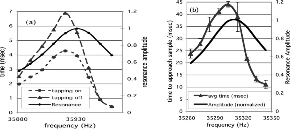
versa for the tapping off. Figure 2.2(a) shows the time response of the model overlaid with
the resonance curve. The time response becomes faster as we move off resonance in either
direction, and the time response for turning the tapping off approaches the time response for
turning the tapping on. At the resonance frequency, the time response for the tapping on
Figure 2. 2: (a) The numerical calculation of the time response for the feedback signal to drop to 1/e for a variety of driving frequencies for two situations: turning the tapping off and turning the tapping on. This time response is overlaid with the resonance curve for reference. (b) The experimental time response for the probe to find the surface with optimized gain given an 8msec-ramped trapezoidal step of height 30 nm.
The dynamic behavior of the probe predicted by the model is consistent with what we
would expect qualitatively. Recall that there are two parameters responsible for the time
response of the system when it is in feedback: the change in damping and the frequency shift,
both can be seen in Figure 2.1. The time response is limited by the width of the resonance
curve, in the sense that if the tip gets too far from the sample, the decay time for the
oscillation scales inversely with the peak bandwidth. Thus the time response is slow due to
the high quality factor (100 to 700) combined with the relatively low resonant frequency
(32-40 kHz). When the probe is close to the sample, the oscillation decreases due to both the
damping of the probe and the frequency shift, and while the damping is slow, the peak shift
is dominant; at probe positions close to the sample, the fast peak shift is dominant. This
inequity results in the two different curves for the cases of tapping on and tapping off. When
the probe is off resonance, the peak shift is dominant, and the time response is faster for both
cases.
In our experiments we clearly see the dynamic behavior predicted by the tapping
model. Without lateral scanning, we apply a 30 nm trapezoidal shaped pulse with an 8 msec
rise and fall time to the z-piezo, which ramps the tip alternately towards and away from the
surface. The probe begins in feedback, so when it moves towards the surface, the tapping is
increased (tapping on), and when it is pulled away from the surface, the tapping is decreased
(tapping off). We maximize the gain until there is no overshoot when the probe retracts as a
reaction to being pushed towards the surface. We plot the time response for the inward
motion of the probe as a reaction to being pulled away from the surface as a function of
driving frequency, and we see a behavior that is very similar to that predicted by the model,
Figure 2.2(b).
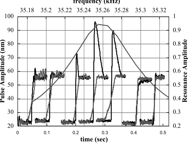
In a second experiment to study the time response of the system, we apply a square
wave to the z-piezo that moves the tip 40 nm alternately towards and away from the surface,
while monitoring the system response. The feedback gain is the same for all frequencies.
We expect the time for the system to respond when the pulse pushes the probe towards
surface to be fast in all cases, pulling the probe away from the surface, due to the increased
tapping. Since the gain is high, overshoot is observed when the ‘ingoing’ response is too
resonance peak). Figure 2.3 shows exactly this behavior. The curves shown are the in and
out motion of the probe with the resonance curve overlaid for reference. As the pulse pulls
the probe away from the surface, the time response for the inward motion, inversely
proportional to the slope, decreases as we increase the driving frequency above the resonance
peak until the time response for the in and out motion of the probe align. This balanced
response quenches the overshoot. If this frequency rather than the peak frequency were used
for feedback, the bandwidth of the NSOM (and SSCM) could be increased 17. Further
increases in frequency much beyond this point result in instability since the damped
resonance curve begins to cross over the free resonance curve.
20 30 40 50 60 70 80 90 100 0.2 0.3 0.4 0.5 0.6 0.7 0.8 0.9 1
0 0.1 0.2 0.3 0.4 0.5
35.18 35.2 35.22 35.24 35.26 35.28 35.3 35.32
Pulse Amplitude (nm) Resonance Amplitude
time (sec) frequency (kHz)
With confidence in a model that accurately describes both the static and dynamic aspects of
our system, we look more closely at the choice for ω1 and β1. Gregor uses the clamped
resonance curve (xc = 0) to determine these values, and they accurately describe the large
frequency shifts and minimal additional damping of his resonance curves as the probe
approaches the sample. Figure 2.4 shows several of our resonance curves including the
0 0 .5 1 1 .5 2 2 .5 3 3 .5 4
3 5.2 35 .4 35 .6 35 .8 3 6 3 6.2
fr eq u e n cy (k H z )
0 0.1 0.2 0.3 0.4 0.5 0.6 Cl am pe d A m pl itu de (m V )
fr e e stp t 0.3 c la m p
Figure 2. 4: Experimental resonance curves showing the undamped resonance, a resonance at 35% of the free resonance and a clamped resonance curve. The peak of the clamped resonance is only 2% of the undamped resonance peak, and the frequency shift is ~400Hz.
clamped curve. The trends are qualitatively different from Gregor's observation. We find
that using the clamped curve to determine ω1 provides values that give a poor fit to our data
because the spring constant is too large. The frequency shift for the clamped peak is 400 Hz
as compared to 60 Hz for the damped peak we use. A simple picture describes both our and
compared to Gregor who is tapping on the sample surface or hard, frozen (low temperature
NSOM) layers. Therefore, we must obtain the parameters for our model from the adsorbed
layer tapping, not surface tapping if we are to describe the dynamics under normal ambient
operation. We note that rather than tapping on the surface adlayers, the probe may be
opening a cavitation hole within the adlayers, resulting in a tapping on the sidewalls of this
cavitation hole. Near a hydrophilic surface, water is structured 18 as are other near-surface
solvents 19, so they are less mobile, indicating that cavitation is likely with the ultrasonic tip
oscillation frequency. Cavitation is also possible with less mobile adsorbates and the less
structured water (clathrates) near a hydrophobic surface 20. Either case, tapping on the
adlayers or cavitating in them, is consistent with our observation of the change in stiffness
that we observe when the probe reaches the sample surface.
If the probe is tapping on the sample surface, then the distance to the sample depends
both on the fiber oscillation amplitude and the angle between the sample and the probe 9.
However, if the probe is tapping on surface adlayers, and the oscillation amplitude of the
probe is much less than the thickness of the adlayer, then the distance to the sample depends
primarily on the thickness of the adlayer and can be accurately controlled, as is the case with
our system. In our studies, the tip does not tap on the hard sample surface (beneath the
adlayers) in the normal operating range, or even closer to the surface, until the probe
oscillation amplitude has decreased due to sample interaction to a few percent of the free
frequency (~1 nm) 17 compared to the 5-10 nm approach curve; the tip simply cannot reach
the surface. As an additional evidence, in our electromigration studies3,4 we have found that
we cannot measure tunnel current between the tip and sample unless we set the feedback
level much below the normal operating range (probe very close to the surface). The process
is repeatable, with minimal tip wear determined by little change in resolution even after
several hours at a low feedback level (tunneling). In the case of small probe oscillation
amplitudes on surfaces with a contamination layer (typical case), shear-force is an accurate
measure of probe-sample separation.
2.2 Data Analysis
In summary, the nonlinear model accurately describes both the system dynamics and
the resonance curve behavior as the probe approaches the sample. During this approach the
probe taps on surface adsorbed layers prior to tapping on the surface itself. This implies that
the lateral force feedback is a good indicator of tip-sample distance when small oscillation
amplitudes are used, and that a tapping mechanism describes the nonlinearity of the
tip-sample interaction. This nonlinear interaction can be used to increase the bandwidth of the
2.3 Bibliography
1. X. Sunney Xie and Robert C. Dunn, Science 265, 361 (1994).
2. E. J. Ayers, H.D. Hallen and C. L. Jahncke, Phys Rev Lett, 85, 4180 (2000).
3. Suzanne Huerth, Michael Taylor, Michael Paesler and Hans Hallen, Proceedings of the
Second Asia-Pacific Workshop on Near-field Optics, Beijing, China, (1999).
4. S. H. Huerth, M. P. Taylor, H. D. Hallen and B. H. Moeckly, Appl. Phys. Lett. 77, 2127
(2000).
5. Khaled Karrai and Robert D. Grober, Appl. Phys. Lett., 66, 1842 (1995).
6. Lapshin, E.E. Kobylkin, V.S. Letokhov, Ultramicroscopy, 83, 17 (2000).
7. M.J. Gregor, P.G. Blome, J. Schöfer and R.G. Ulbrich, Appl. Phys. Lett., 68, 307 (1996).
8. I.I. Smolyaninov, W. A. Atia, A Pilevar, CC Davis, Ultramicroscopy, 71, 177 (1998).
9. Kate Hsu and Levi A. Gheber, Rev. Sci. Inst., 70, 3609 (1999).
10. P.K. Wei and W.S. Fann, J. Appl. Phys., 83, 3461 (1998).
11. J. U. Schmidt, H. Bergander, and L. M. Eng, J. Appl. Phys., 87, 3106 (2000).
12. P.K. Wei, W.S. Fann, J. Appl. Phys., 87, 2561 (2000).
13. R. Brunner, O. Marti, and O. Hollricher, J. Appl. Phys, 86, 7100 (1999).
14. Khaled Karrai and Ingo Tiemann, Phys. Rev. B, 62, 13174 (2000).
15. C. Durkan, and I.V. Shvets, J. Appl Phys., 79, 1219 (1996).
16. Michael Muto, M.S. Thesis, North Carolina State University, (1997).
18. R. M. Pashley and J. A. Kitchener, J. Colloid and Interface Sci., 71, 491 (1979).
19. R.G. Horn and J. Israelachvili, J. Chem. Phys., 75, 1400 (1981).
Chapter 3
3. Imaging Techniques of Irregular
Surfaces
3.1 Introductory NSOM
Paints are industrially important materials; quality control requires detection of the
defect, and corrective action requires knowledge of the cause. To identify the defects, we
propose nanometer to micrometer regime (mesoscale) optical and topographical surface
characterization. In particular, a unique approach is presented for identifying and
characterizing surface features through the use of NSOM. NSOM enables optical and
topographical imaging of mesoscale surface features through high-resolution imaging 1, 2.
brought within nanometers of a sample surface and rastered while the topographical and
optical signal are simultaneously collected 4, 5. The statistical analysis of these observations
characterizes surface features such as clumping, pigment density fluctuations, and overall
smoothness of sample surfaces. In addition, individual pigment particles can be identified.
Two types of samples were imaged and defined as follows: a reference sample, R, of high
quality and a low quality sample, N. The quality value is based upon visual inspection. This
study of the samples shows that quality variations are differentiated at the mesoscopic length
scales over which both the optical and topographic signals vary. A histogram of the
variations shows a peak at a mesoscopic length for the R sample, while it continues to
increase at smaller distances for the lower quality sample, N. Thus, the length scale of the
fluctuations is more important for observing paint quality than actual fluctuations.
3.2 Imaging Methods
NSOM microscopes enable the extension of optical techniques for higher resolution
imaging5, 6. In order to obtain high-resolution images, the system must be free of vibrational
noise, the tip must be close to the sample, and stable feedback must be established 2. In our
system, shear-force feedback is the method of probe sample distance control 7, 8. The NSOM
setup uses a tuning fork oscillator to detect the tip oscillation amplitude and control the
separation of the tip and sample 6. Shear force feedback uses voltage generation by a quartz
crystal tuning fork to measure the oscillation amplitude that varies with distance 7, 8. Fiber
tuning fork9. The tuning fork's resonance frequency is altered by the presence of the mounted
probe 4. The frequency changes from ~33 kHz to ~40 kHz due to stiffening of the mechanical
oscillator (tuning fork and fiber). Once the probe is close to the sample surface, there is a
change in resonance frequency and the oscillation amplitude decreases 1. The nonlinear
tapping interaction between the probe and layers adsorbed on the sample is used to increase
the operational bandwidth of this high quality factor oscillation system 7. To identify
pigment distributions and individual particles, topographical and optical data were collected.
For collection of topographical information, the optical probe raster scans across the
specified scan range under z feedback collecting forward and backward data (in both
directions) on the contour of the sample 6, 10. The forward and backward images are
correlated to insure artifact-free imaging and to determine noise levels 11. For collection of
optical data, a collection lens relays reflected light into a photomultiplier tube (PMT). Both
the PMT and collection lens are located at a 45 degree angle to the sample surface normal.
HeNe laser light (532.8nm) coupled into the optical probe is used for sample illumination.
Both forward and backward optical images are correlated during analysis.
3.3 Imaging Results
Several areas on each of the reference and low quality sample were imaged and
compared. The topographic images required background subtraction calculated from a least
squares fit to a sub region of the image. It corrects for an overall tilt of the sample. Multiple
to distinguish between artifacts and actual structures. Artifacts will not be repeated in both
forward and backward data, but real features will 12, 13. In analyzing forward and backward
line cuts, a hysteresis is visible in the data due to inherent losses in the piezo-tube scanner
during the lateral scanning process 14. This phenomena is well identified and anticipated in
these large scans, so it does not cause discrepancies in image analysis.
Figures 3.1 and 3.2 are images of the reference sample. Aligned, uniform circular
structures can be seen, as expected from the reference sample. In Figure 3.2, it is possible to
see the ridging of the polymer in the lower right corner of the image. The image scale ranges
from white (highest point value) to black (lowest point value) with a distance range of 1920
nanometers, which is also the distance range for Figure 3.1. Similarities in the optical and
topographical images indicate a coupling between topography and pigment distribution. Due
to the large size scale and comparison of forward and backward images, we know that this is
not a NSOM ‘topographical artifact’ but rather a real coupling between pigment density and
topography 12, 15. Knowing that we are able to resolve on a scale range near that of the
pigment particles and identify what we believe to be the polymer structure, we focus on
discriminating between the reference and low quality sample. We recorded and plotted the
long and short term height variations in the two paint samples. Short term variations are
defined as variations over a 300-500 nm length scale (one quarter the image size), and long
term variations are defined as variations over the interval of the entire image range (1-2 µm).
Overall, 62 images (optical and topographical) were evaluated for long and short term
each long and short scale variation, two numbers were recorded; the first is the variation
defined above and the second is the maximum average value in the image. The percent
variations were obtained by dividing the first number by the second and multiplying by 100.
The reason for normalization is to correct for variations of laser power or probe through-put
in various images.
Figure 3. 1: This is a topographic scan of the reference sample (1905nm x 1905nm). The axes are in
nanometers. The overall z distance range is 1138nm. The middle region of the image represents one plateau at a vertical position near 228nm. The upper middle portion of the image is 187nm above the middle plateau, and the bottom right where polymer ridging is observed is 663nm below the middle plateau.
The throughput is highly probe-dependent, and normalization allows quantitative
comparisons of data from different probes. These ratios (long and short scale) were plotted
times showing pigment particles, but in non-uniform arrangements. There is no identifiable
arrangement, but particle clumping was observed in Figure 3.3. From the histograms (Figure
3.4), we note the Reference, R, data are strongly peaked at low percent variation, whereas the
low quality samples, N, show a much wider range in variation on all length scales ranging
from very small variations (peak near zero) to large variations (beyond the peak of R).
Figure 3. 2: This is an optical scan of the reference sample (1905nm x 1905nm). The optical range was measured in arbitrary units. The horizontal axis is in nanometers. There is an overall optical range of 0.051a.u. In the upper left and lower right portions of the image, polymer ridging is observed. This is consistent with Figure 3.1, which was taken over the same scan range.
That is, the Reference data are strongly peaked at a nonzero low variation, and drop sharply
to zero, whereas the low quality samples decrease from a maximum near zero and exhibit a
Figure 3. 3: This is an optical scan of the low quality sample (3175nm x 3175nm). The horizontal axis is in nanometers. There is an overall optical range of 0.27a.u. The scan shows pigment particle clumping in a non-uniform manner. Although the arrangement is non-non-uniform, it is still possible to identify pigment particles (see Figure 3.5).
3.4 Single Pigment Particle Imaging
Individual pigment particles were identified in several scans. Evidence of these
single particles can be found in an image by expanding small regions of the images and
data. The line cut data allows us to look at z versus x or y, all measured in nanometers. It is
free from color-table induced artifacts and elucidates the noise levels.
0 0.5 1 1.5 2 2.5 3 3.5 4 4.5
0 20 40 60
Variation (nm) Nu m be r N short R short N long R long 0 2 4 6 8 10 12
0 200 400 600
Variation (nm)
Nu
m
be
r
N short R short N long R long
Figure 3. 4: (a) is a histogram of the optical variation and (b) a histogram of the topographical variation. In analyzing the percent variation, it is possible to distinguish between the reference and low quality sample.
Correlations of peaks in the forward and backward data of the optical and topographical
scans permit identification of single pigment particles. The particles identified were 20-30
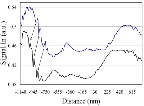
nm in half-height diameter, which is approximately our optical resolution. Figure 3.5 shows (a)
the optical data in which arrows indicate the points that represent individual pigment
particles, and we can identify the positions of various single particles that were resolved.
There is a noticeable hysteresis in the forward and backward data which is due to lateral drift
in the piezo-electric tube used for fine (x,y,z) adjustment 14. The same particles were verified
in the topographical data.
0.38 0.42 0.46 0.5 0.54
-1140 -945 -750 -555 -360 -165 30 225 420 615
Distance (nm)
S
ig
na
l I
n
(a
.u
.)
Figure 3. 5: This is the optical forward/backward line-cut data from the lower portion of Figure 3.3. The forward data have been shifted upward for clarity. The horizontal axis is distance (nm), and the vertical axis is in arbitrary units. The forward data (top graph) is shifted to the right of the back data (bottom graph) due to hysteresis. The arrows indicate corresponding data points in the forward and backward data that reflect the same pigment particles.
3.5 Data Analysis
Pigment particles near the sample surface were imaged with NSOM. Images of polymers in
the paint sample also identified large scale structures such as ridged or clumped orientations.
and also non-uniform particle clumping. Statistical analysis of paint sample images yields
information about the mesoscale order of the pigment distributions. The histograms (Figure
3.4) illustrate our approach using the long and short term variations to distinguish between
the low and high quality samples. The NSOM approach for sample identification and
characterization was effective in allowing us to resolve features in the mesoscale regime,
3.6 Bibliography
1. C.L. Jahncke and H. D. Hallen, J. Appl. Phys. 93, 1274 (2003).
2. E. Betzig and J. Trautman, Science 257, 189 (1992).
3. A. Lazerev, N. Fang, Q. Luo, and X. Zhang, Rev. of Sci. Instrum. 74, 3679 (2003).
4. K. Karrai and R. Grober, Proceedings of SPIE, edited by Michael A. Paesler and
Patrick J. Moyer 2535, 69 (1995).
5. R. Brunner, A. Bietsch, O. Hollricher, O. Marti, Rev. Sci. Instrum. 68, 1769 (1997). 6. J. Hsu, Mat. Sci. Engin. 33, 1 (2001).
7. C.L. Jahncke, S.H. Huerth, Beverly Clark III, and H.D. Hallen, Appl. Phys. Lett. 81, 4055 (2002).
8. K. Karrai and R. Grober, Appl. Phys. Lett. 66, 1842 (1995).
9. D. Davydov, K. Shelimov, T. Haslett, M Moskovits, Appl. Phys. Lett 76, 1796 (1999). 10. M. A. Paesler, P.J. Moyer, Near-field Optics: Theory, Instrumentation, and
Applications, Wiley & Sons (1996).
11. O. Fenwick, G. Latini, F. Cacialli, Synthetic Materials 147, 171 (2004). 12. S. Bozhevolnyi, J. Opt. Soc. Amer. B 14, 2254 (1997).
13. X. Wang, Z. Fan, T. Tang, J. Opt. Soc. Amer. A 22, 2730 (2005).
14. D. Croft, G. Shed, S. Devasia, J. of Dyn. Syst., Meas., and Contr.123, 35 (2001).
Chapter 4
4. Novel Split-Tip Proximal Probe for
SSCM and Fabrication of
Nanometer-Textured, In-Plane Oriented Polymer Films
4.1 Introduction
Many complex materials, polymers, or molecular-based electronic devices depend
upon the orientation of the components for their properties. This requirement places severe
constraints on deposition techniques when lateral resolution on the nanometer length scale is
required. We describe the fabrication of a scanning probe that can be used to deposit polymer
self-assembled monolayers, SAMs, for which the orientation is perpendicular to the surface,
and obviates the need for deposition of an electrode on top of the SAM polymer molecules.
The latter process is difficult and often results in damage or destruction of the SAM due to
the energy carried by the deposited species 2, 3. The probe enables new device structures,
since it can reverse the orientation of deposited, non-symmetric molecules with nanometer
resolution. The result will be a potential barrier at the interface, which can be gated to
provide device operation.
This dissertation presents the fabrication and electric connection methods of the
central tool to enable this technique: the split-tip probe. It is built on a sharpened optical
fiber. The fabrication process is not obvious; we show that methods developed for
fabrication of near-field scanning optical microscope (NSOM) probes do not work well for
fabrication of split-tips. The primary reason for failure is film stress and shorting problems.
We model and demonstrate how these methods can be modified to successfully produce
split-tips. The electrical connection to the probes is also difficult due to the requirement of
multiple connections without shorting (to a thin film on a 125 micron diameter fiber), while
simultaneously mounting the fiber for successful lateral force microscopy to allow the use of
the split-tip on a scanning proximal probe microscope system. Another application of the
probe is in Split-tip Scanning Capacitance Microscopy (SSCM), a novel electrical
characterization tool in which the capacitance between the split-tip electrodes is measured.
Additionally, information about the local sample conductivity is obtained (in a non-contact
microscope, consists of two electrically isolated and independently contacted metal
electrodes deposited on opposite sides of a tapered optical fiber, similar to those used for
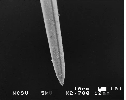
NSOM 4, 5. An electron microscope image of a split-tip probe is shown in Figure 4.1.
Aluminum (Al) or gold (Au) is used in these tips for electrodes and ultraviolet light
confinement. A NSOM system has the required optical capability for coupling laser light
down the fiber into the region between the split-tip electrodes, which is exactly where it is
needed for initiating the deposition to the surface.
Figure 4. 1: The split-tip probe has electrodes on the left and right sides, and the aperture located at the bottom.
The probe not only guides the deposition, but can characterize the quality of the resulting
material by the following: measurement of topography by the NSOM-like scanning probe 6,
measurement of orientation with polarization-dependent NSOM imaging with the split-tip
The key parameter for metal deposition is film stress. The most important factor for
electrical isolation is the advantageous use of diffusion and island growth (Au) or oxidation
(Al) in the regions between the electrodes. The major concern for mounting is that the thin
film not be wiped off by the contact metal.
4.2 Probe Fabrication Methods
We first describe the oriented molecular deposition scheme used and some of the
other criteria that impact the design of the probe, then detail the probe fabrication steps.
4.2.1 Probe Design Criteria
A schematic of the split-tip probe near the sample as molecules are being deposited
with a fixed orientation to the sample surface is shown in Figure 4.2. In this cut-away view,
the electrodes are on the left and right sides of the tip.
100 nm
Tapered Optical Fiber
Metal Coating, 2 sides
Oriented Molecules Random Orientation
V I
Electric Field
The electric field is localized in the region of the split, and is highest where the split is
narrow (near the tip apex). Molecules that are in solution will be oriented and deposited
where the field is high, but not elsewhere. When the tip moves to a new location, it aligns
the molecules, then initiates the deposition to the sample with a pulse of ultraviolet light.
The tip then moves to a new location, orients the molecules as they should be in the new
location, and links them to the surface. It is important that molecules not under the probe
aperture not attach to the surface, since they are not oriented. The scheme we have used is to
spin a wet layer onto the surface, by exposing the regions for deposition while the molecules
are rotated by the field, and then wash the remainder off. Another alternative is to load the
tip with molecules as in the ‘dip-pen’ lithography scheme, oriented and attached as in liquid,
then another molecule chosen for a different position 7. These schemes have the same
requirements for the probe. The requirements for the split-tip probe are as follows: the two
electrodes must be electrically isolated from each other, the ultraviolet light must be able to
propagate through the probe to the region between the electrodes, the deposition must not
occur on the probe itself, the probe must be compatible with a microscope system, the probe
must not be ‘shorted’ by the solution or the molecules that are in the solution, the probe must
be usable in a probe-surface distance regulation scheme, and the probe should have a
reasonable lifetime.
4.2.2 Probe Fabrication
The split-tip probe fabrication begins with sharpening an optical fiber using a process
modified to work better with fibers, 8, 9, 10, 11 or chemical etching 12 to taper the end of an
optical fiber. Pulling fibers is needed when a large separation of the electrodes is desired,
since the fiber gets a flat face as it cleaves in the fiber pulling apparatus, as can be seen in
Figure 4.3. This shape contrasts with the sharp point (few nm radius) at the tip of properly
etched fibers. Thus, if the electrodes are to be brought in close proximity of the surface, they
need to be close together with etched fibers, but may be further apart when pulled fibers are
used. Etched fibers are more reproducible to fabricate in large quantities, and have a higher
optical throughput.
Figure 4. 3: SEM image of a larger-aperture tapered fiber fabricated by the heat-and-pull method. Note the flat cleaved end that is formed when this fabrication scheme is used, as opposed to the sharp point of etched fibers.
Once the fibers are shaped, metal is coated onto one side; then the fiber is rotated
180°, and the other electrode is deposited. This forms a split metal structure with the two
metal sides electrically isolated. The metal coating must be thin (~5nm) so that the two sides
do not short together. The probe-holding fixture mounts inside the deposition chamber,
from the chamber. The probes are mounted on holders that keep the probes straight and
separated by a sufficient distance to ensure they do not shadow each other during
evaporation. Between 8 and 10 probes are held in each unit. Two units can be used at once
in the evaporator system, oriented to face each other. The probe holder is mounted on a large
gear, and the fiber tails run through a series of holders, also mounted on the gear, in the
direction to prevent unraveling during rotation. The gear is turned by an electric motor. We
have found that the motors work reliably in vacuum when they are driven by a voltage lower
than their maximum rating. Although it is commonly known that the back-voltage generated
by the motor limits the current and lower voltages result in motor over-current failure, we
have found that the current is limited primarily by the resistance of the wires when these
small motors are under load. Motor failures are usually the result of shorting from metal
deposition or an increase in friction in the mechanism, often due to effects of metal
deposition. Copper braiding connects the axle of the larger gear shaft to a liquid nitrogen cold
trap mounted directly over the rotation units. In this way, the fibers can be cooled by
radiation (with approximately pi-steradians of solid angle towards the cold trap) and by
conduction through the copper braids, shaft, gear, holder, and fiber shanks. The evaporation
chamber allows three different source materials to be used during one pump-down; Al and
Au are commonly used for split-tips. Following the initial Al or Au deposition, a thicker
coating (~100nm) of gold is applied to the contact regions on the shank of the tip. A small
source, so that the shanks are coated with metal. A close-up SEM view of the split-tip probe
can be seen in Figure 4.1, and a view at higher magnification is given in Figure 4.4.
Figure 4. 4: The end of a split-tip fabrication with the optimal fabrication procedures.
4.2.3 Probe Mounting
The split-tip probe needs independent electrical contact to each side. Due to the concerns
noted above, contact and lack of shorting between the two sides must be verified. Thus, two
metal contacts are made to each side. Furthermore, the probe must be compatible with
mounting into a scanning proximal probe microscope such as NSOM or SSCM systems. The
latter entails mounting the probe tip onto the side of a quartz tuning fork (a few mm in
length, with 32768 Hz free resonance) that is mounted to the microscope5, 13. To prevent
shear from removing the metal layer near the contacts, the fiber must be held securely in
place, without translation or rotation. Our system allows for these constraints by rigidly
holding the fiber in a V-groove/clamp with 2 gold wires pressed against each side. This is
hemispheres attached to the bottom of the glass plate. The V-groove allows the s plit-tip
probe to rest securely keeping the lower electrode of the probe positioned on the metal
contacts.
There is an additional Teflon cover secured by screws providing contacts to the top split-tip
electrode. This Teflon fixture can be translated and rotated with three screws to bring the
fiber probe up against the tuning fork. Both the fixture and tuning fork are mounted to a
glass plate (Figure 4.5) that fits onto the scanning probe microscope, so that mounting can be
performed conveniently away from the scanning probe microscope, under a dissection
microscope. Once the probe is against the tuning fork, glue is applied to the joint and the
adjustments left fixed. A drop of epoxy applied to the base of the tuning fork improves
stability.
We have found that the clamping of the fiber as shown in Figure 4.5 does not impair
the lateral force microscopy as used in NSOM 13. Also, there have been no observed
significant differences in the resonance behavior of the split-tips compared to uncoated or
uniformly-coated NSOM probes.
4.2.4 Probe Usage
The operating sequence once the probe is mounted begins with verifying that contact
is established on both sides by measuring the resistance between the wires on the same side
of the probe with a multimeter. When both sides have contact, the resistance between the two
sides is measured, and should be too large for the meter to register. Possible causes of a
lower resistance include a twisting of the probe so that the split is shorted at the contact
wires, or a probe short near the tip, formed during the deposition of the metal. The latter
typically occurs when there is an etching defect that leaves a mound or hollow on the taper
the edge of the mound. Shorting can happen if Al probes are not sufficiently oxidized. It is
possible to measure the resistance from one wire on the holder to the fiber coating itself, by
using a thin (0.002 inch diameter) gold wire to make the contact to the coating. However, this
contact is not as reliable as a fixed contact. Once the electrical characteristics of the probe
and connections are verified, a variable voltage is applied to the probe. We sometimes
replace the ground lead with the virtual ground of a high gain current preamplifier, to
monitor the magnitude of any shorting current as a more discriminating detector of shorts.
4.3 Results & Discussion
A significant challenge in the fabrication process is the production of a well defined split and
a smooth continuous coating of metal all the way to the aperture of the probe. This is much
less difficult for NSOM probes since the metal forms a continuous ring around the diameter
of the NSOM probe. If there is stress in the metal layer, the film itself will hold the stress.
When the metal is thermally evaporated, the stress is typically tensile 14. This means that the
metal will try to pull itself apart from the probe. If the metal is continuous, it will pull on
itself, and usually remain stable. On the split tip, the metal is not continuous; so the stress
must be held by the interface between the film and the underlying silica. Far from the tip,
this is possible since the area is large; but as the tip is approached, the area is reduced and the
curvature increased. The series of SEM micrographs in Figure 4.6 illustrate this. There
appears to be a near perfect split in our split tip at low magnification, Figure 4.6(a). It is
Approaching the probe aperture, at 2000 times magnification, Figure 4.6(b), shows cracking
and peeling, which presents a significant problem. Figure 4.6(c) shows the probe at 11,000
times magnification, clearly indicating problems with tensile stress 15, 16. The aluminum film
on the right side of the split tends to bow in a few regions. It is also seen from this
micrograph that tensile stress will relieve itself through micro cracking of the film and
peeling of the cracked surface from the substrate. The stress distribution in this film is
anisotropic; cracking patterns depend on the stress distribution.
Figure 4. 6: (a) shows split-tip probe fabricated with certain imperfections, such as voids in the coating. (b) shows cracking and peeling which presents a significant problem. (c) shows tensile stress.