IJEDR1402263
International Journal of Engineering Development and Research (www.ijedr.org)2835
A Novel Approach For the Design and
Implementation of FPGA Based High Speed Digital
Modulators Using Cordic Algorithm
1
Dhivya Jose,
2Reneesh C Zacharia
,
3Rijo Sebastian
1
M Tech student, 2,3Assistant Professor 1 Department of ECE
1Mangalam college of Engineering, ettumanoor, Kottayam, India
________________________________________________________________________________________________________
Abstract— The main objective of this paper is to implement all digital modulation techniques into a single module and
implement in a Field Programmable Gate Array (FPGA). The proposed system allows the user to select any one of four modulations without reconfiguring the FPGA. Carrier waveform for the modulator is generated using coordinate rotation digital computer CORDIC algorithm which uses shift, addition and very small look up table (LUT). It is hardware efficient and iterative algorithm for circular rotation and an efficient method to compute trigonometric functions. The codes for these digital modulators are developed in VHDL and the functionality of these digital modulators was simulated using the MODELSIM simulation software and synthesized by Xilinx ISE Design suite14.5 and finally implemented in SPARTAN-3E FPGA.
Index Terms— Binary amplitude shift keying (BASK) , Binary phase shift keying (BPSK), Binary frequency shift keying
(BFSK), Quadrature phase shift keying (QPSK) ,Field Programmable Gate Array,(FPGA),CORDIC
________________________________________________________________________________________________________
I.INTRODUCTION
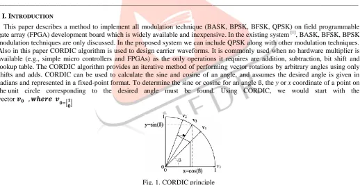
This paper describes a method to implement all modulation technique (BASK, BPSK, BFSK, QPSK) on field programmable gate array (FPGA) development board which is widely available and inexpensive.In the existing system [1], BASK, BFSK, BPSK modulation techniques are only discussed. In the proposed system we can include QPSK along with other modulation techniques. Also in this paper CORDIC algorithm is used to design carrier waveforms. It is commonly used when no hardware multiplier is available (e.g., simple micro controllers and FPGAs) as the only operations it requires are addition, subtraction, bit shift and lookup table. The CORDIC algorithm provides an iterative method of performing vector rotations by arbitrary angles using only shifts and adds. CORDIC can be used to calculate the sine and cosine of an angle, and assumes the desired angle is given in radians and represented in a fixed-point format. To determine the sine or cosine for an angle ß, the y or x coordinate of a point on the unit circle corresponding to the desired angle must be found. Using CORDIC, we would start with the vector [ ]
Fig. 1. CORDIC principle
In the first iteration, this vector is rotated 45° counterclockwise to get the vector. Successive iterations rotate the vector in one or the other direction by size-decreasing steps, until the desired angle has been achieved. Step size denoted by i is arctan(1/(2i−1)) for i = 1, 2, 3, every iteration calculates a rotation, which is performed by multiplying the vector with the rotation matrix
= -1.
The rotation matrix is given by:
=[ ] (1) Using the following two trigonometric identities:
√ (2)
IJEDR1402263
International Journal of Engineering Development and Research (www.ijedr.org)2836
The expression becomes:[ ] [
] (6) Where
√
And can have the values of −1 or 1, and is used to determine the direction of the rotation; if the angle is positive then is +1, otherwise it is −1.
( ) ∏ ∏
√ ⁄
(7)
Which is calculated in advance and stored in a table, or as a single constant if the number of iterations is fixed. This correction could also be made in advance, by scaling and hence saving a multiplication.
II.DIGITAL MODULATORS
A.BPSK
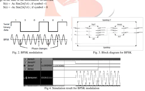
In BPSK we change the phase of the sinusoidal carriers to indicate information. Phase in this context is the starting angle at which sinusoid starts .To transmit 0, we shift the phase of the sinusoid by 180ºas shown in Fig .2 Phase shift represents the change in the state of the information. In this case
S(t) = Ac Sin(2𝜋𝑓𝑐𝑡) ; if symbol =1 S(t) = -Ac Sin(2𝜋𝑓𝑐𝑡) ; if symbol = 0
Fig. 2. BPSK modulation Fig. 3. Block diagram for BPSK
Fig 4. Simulation result for BPSK modulation B.BASK
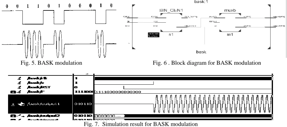
In BASK, the amplitude of the signal is changed in response to information and all else is kept fixed .Bit 1 is transmitted by a signal of one particular amplitude .To transmit 0, we change the amplitude keeping the frequency constant .On –Off Keying (OOK) is a special form of ASK, where one of the amplitude is zero as shown in Fig .5 below. BASK signal can be represented as
IJEDR1402263
International Journal of Engineering Development and Research (www.ijedr.org)2837
Fig. 5. BASK modulation Fig. 6 . Block diagram for BASK modulationFig. 7. Simulation result for BASK modulation C.BFSK
In FSK, we change the frequency in response to information, one particular frequency for a 1 and another frequency for a 0 as shown in Fig.8. In the example frequency f1 for bit 1 is higher than f2 used for a 0 bit. In general it is called m-array FSK. When m is two then it s called binary –FSK with two carriers. A BFSK signal is represented as
S(t) = Ac Sin(2𝜋𝑓1𝑐𝑡) ; if symbol = 1 S(t) = Ac Sin(2𝜋𝑓2𝑐𝑡) ; if symbol = 0
Fig.8. BFSK modulation
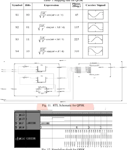
Fig .9. Block diagram for BFSK modulation Fig.10. Simulation result for BFSK modulation D . QPSK
IJEDR1402263
International Journal of Engineering Development and Research (www.ijedr.org)2838
Fig. 11. RTL Schematic for QPSK
Fig. 12. Simulation result for QPSK
IJEDR1402263
International Journal of Engineering Development and Research (www.ijedr.org)2839
Fig.13. Flow ChartIII.CONTROLUNIT
In control unit, for controlling given data, the multiplexers are used.
Table-2 Control unit information
SL
NO CONTROL BIT
MODE OF OPERATION
1 00 BASK
2 01 BFSK
3 10 BPSK
4 11 QPSK
Fig.14. Block diagram of Ingrated Digital Modulators
IJEDR1402263
International Journal of Engineering Development and Research (www.ijedr.org)2840
Fig.17. Power Vs Voltage graph for modulation Fig. 18. Power Vs voltage graph for modulation using CORDIC
ALGORITHAM
Table 3 Power and delay for modulation
POWER(WATTS) 0.063
DELAY(ns) 11.860
Table. 4. Power and delay for modulation using CORDIC algorithm
POWER(WATTS) 0.076
DELAY(ns) 10.928
IV.CONCLUSION
FPGA implementation of BASK, BPSK, BFSK, and QPSK modulators were implemented. The main advantage of this proposed method is the integration of all the basic digital modulators in a single module and can generate carrier signal using CORDIC algorithm thereby avoiding hardware multipliers which are the major power consuming element in digital design. REFERENCES
[1] C. Erdoğan, I. Myderrizi, and S. Minaei,(2012,april) “FPGA Implementation of BASK-BFSK-BPSK Digital Modulators” Proceedings of the IEEE Antennas and Propagation Magazine, Vol. 54, No. 2
[2] Asraf Mohamed Moubark,Mohd Alauddin Mohd Ali ,Hilmi Sunusi,(2013,jan)” FPGA implementation of low power QPSK modulator using verilog HDL”Journal of applied sciences 13(3):385-392,2013.
[3] B. Alecsa, and A. Onea,( December 12-15,2010) “Design, Validation and FPGA Implementation of a Brushless DC Motor Speed Controller,” Proceedings of the 17th IEEE International Conference on Electronics, Circuits, and Systems (ICECS), , pp. 1112-1115.
[4] Asraf Mohamed Moubark,Mohd Alauddin Mohd Ali ,Hilmi Sunusi “ Simple QPSK Modulator Implemented in Virtex 6 FPGA Board for Satellite Ground Station”