Black-Box Parallel Garbled RAM
∗Steve Lu† Rafail Ostrovsky‡
In 1982, Yao introduced a fundamental technique of “circuit garbling” that became a central building block in cryptography. Recently, the question of garbling general random-access memory (RAM) programs received a lot of attention in the literature where garbling an encrypted data can be done separately from garbling program(s) that execute on this (garbled) RAM. The most recent results of Garg, Lu, and Ostrovsky (FOCS 2015) achieve a garbled RAM with black-box use of any one-way functions and poly-log overhead of data and program garbling in all the relevant parameters, including program run-time. The advantage of their solution is that large data can be garbled first, and act as persistent garbled storage (e.g. in the cloud) and later programs can be garbled and sent to be executed on this garbled database in a non-interactive manner.
One of the main advantages of cloud computing is not only that it has large storage but also that it has a large number of parallel processors. Despite multiple successful efforts on parallelizing (interactive) Oblivious RAM, the non-interactive garbling of parallel programs remained open until very recently. Specifically, Boyle, Chung and Pass in their upcoming TCC 2016 paper (see their recently updated eprint version [3]) have recently shown how to garbled PRAM program with poly-logarithmic (parallel) overhead assuming non-black-box use of identity-based encryption. The question whether such a strong assumption and non-black-box use of such a strong assumption are needed. In this paper, we resolve this important open question and show how to garble parallel programs, with only black-box use one one-way functions and with only poly-log overhead in the (parallel) running time. Our result works for any number of parallel processors.
Keywords: PRAM; Garbled RAM; Black-Box Cryptography; One-Way Functions; Secure Computation
∗
This material is based upon work supported in part by DARPA Brandeis program under Contract N66001-15-C-4065. The views expressed are those of the author and do not reflect the official policy or position of the Department of Defense or the U.S. Government.
†
Stealth Software Technologies, Inc. [email protected]
‡
1
Introduction
Yao [17] introduced a technique allows one to “garble” a circuit into an equivalent “garbled circuit” that can be executed (once) by someone else without understanding internal circuit values during evaluation. A drawback of circuit representation (for garbling general-purpose programs) is that one can not decouple garbling encrypted data on which the program operates from the program code and inputs. Thus, to run Random Access Machine (RAM) program, one has to unroll all possible execution paths and memory usage when converting programs into circuits. For programs with multiple “if-then-else” branches, loops, etc. this often leads to an exponential blow-up, especially when operating on data which is much larger than program running time. A classic example is for a binary search overnelements, the run time of RAM program is logarithmic innbut the garbled circuit is exponentially larger as it hasn size since it must touch all data items.
An alternative approach to program garbling (that does not suffer from this exponential blowup that the trivial circuit unrolling approach has) was initiated by Lu and Ostrovsky in 2013 [15], where they developed an approach that allows to separately encrypt data and separately convert a program into a garbled program without converting it into circuits first and without expanding it to be proportional to the size of data. In the Lu-Ostrovsky approach, the program garbled size and the run time is proportional to the original program run-time (times poly-log terms). The original paper required a complicated circular-security assumption but in sequence of follow-up works [15,10,9,7] the assumption was improved to a black-box use on any one-way function with poly-logarithmic overhead in all parameters.
Circuits have another benefit that general RAM programs do not have. Specifically, the circuit model is inherently parallelizable - all gates at the same circuit level can be executed in parallel given sufficiently many processors. In the 1980s and 1990s a parallel model of computation was developed for general programs that can take advantage of multiple processors. Specifically, a Parallel Random Access Memory (PRAM), can take advantage of m processors, executing all of them in parallel withm parallel reads/writes. The question that we ask in this paper is this:
Can we construct garbled Parallel-RAM programs with only poly-logarithmic (parallel) overhead making only black-box use of one-way function?
The reason this is a hard problem to answer is that now one has to garble memory in such a way that multiple garbled processor threads can read in parallel multiple garbled memory locations, which leads to complicated (garbled) interactions, and remained an elusive goal for these technical reasons. In this paper we finally show that this is possible to achieve. Specifically, we show an optimal result both in terms of cryptographic assumptions and the overhead achieved: we show that any PRAM program with persistent memory can be compiled into parallel Garbled PRAM program (Parallel-GRAM) based on only a black-box use of one-way functions and with poly-log (parallel) overhead. We remark that the techniques that we develop to achieve our result significantly depart from the work [7].
1.1 Problem Statement
Suppose a user has a large database D that it wants to encrypt and store in a cloud as some garbled ˜D. Later, the user wants to encrypt several PRAM programs Π1,Π2, . . . where Πi is a
parallel program that requires m processors and updates ˜D. Indeed, the user wants to garble each Πi and ask the cloud to execute the garbled ˜Π program against ˜D using m processors. The
up-to-dateD.) At the same time, we requireprivacywhich means that nothing but each program’s running time and the output are revealed. Specifically, we require a simulator that can simulate the parallel program execution for each program, given only its run time and its output. The simulator must be able to simulate each output without knowing any future outputs. We measure the parallel efficiency in terms of garbled program size, garbled data size, and garbled running time.
1.2 Comparison with previous work
In the interactive setting, a problem of securely evaluating programs (as opposed to circuits) was started in the works on Oblivious RAM by Goldreich and Ostrovsky [12, 16, 13]. The work of non-interactive evaluation of RAM programs were initiated in the Garbled RAM work of Lu and Ostrovsky [15]. This work showed how to garble memory and program so that programs could be non-interactively and privately evaluated on persistent memory. Subsequent works on GRAM [10,
9,7] improved the security assumptions, with the latest one demonstrating a fully black-box GRAM from one-way functions.
In a highly related sequence of works, researchers have also worked in the setting where the garbled programs are also succinct or reusable, so that the size of the garbled programs were independent of the running time. Gentry et al. [11] first presented a scheme based on a stronger notion of different inputs obfuscation. At STOC 2015, works due to Koppula et al. [14], Canetti et al. [5], and Bitansky et al. [2], each using different machinery in clever ways, made progress toward the problem of succinct garbling using indistinguishability obfuscation. Recently, Chen et al. [6] and Canetti-Holmgren [4] achieve succinct garbled RAM from similar constructions.
The first work on parallel Garbled RAM was initiated in the paper of Boyle, Chung and Pass [3] where they study it in the context of building an Oblivious Parallel RAM (this work, along with another paper on Oblivious Parallel RAM by Chen, Lin, and Tessaro is among the TCC 2016 accepted papers). In that paper they show how to construct garbled PRAM assuming non-black-box use of identity-based encryption. That is, they use the actual code of identity-based encryption in order to implement their PRAM garbled protocol. In contrast, we achieve black-box use of one-way functions only, and while maintaining poly-logairhmic (parallel) overhead (matching classical result of Yao for circuits) for PRAM computations. One of the main reasons of why Yao’s result is so influential is that it used one-way function in a black-box way. Black-box use of a one-way function is also critical because in addition to its theoretical interest, the black-box property allows implementers to use their favored instantiation of the cryptographic primitive: this could include proprietary implementations or hardware-based ones (such as hardware support for AES).
1.3 Our Results
In this paper, we provide the first construction of a fully black-box garbled PRAM, i.e. both the construction and the security reduction make only black-box use of any one-way function.
1.4 Overview of our construction
There are several technical difficulties that must be overcome in order to construct a parallelized GRAM using only black-box access to a one-way function. One attempt is to take the existing black-box construction of [7] and to apply all m processors in order to evaluate their garbling algorithms. However, the problem is that due to the way those circuits are packed into a node: a circuit will not learn how far a child has gone until the the predecessor circuit is evaluated. So there must be some sophisticated coordination as the tree is being traversed or else parallelism will not help beyond faster evaluation of individual circuits inside the memory tree. Furthermore, circuits in the tree only accommodates a single CPU key per circuit. To take full advantage of parallelism, we have the ability to evaluate circuits that are much wider and holds more CPU keys. However, we do not know apriori where these CPUs will read, so we must carefully balance the width of the circuit so that it is wide enough to hold all potential CPU keys that gets passed through it, yet not be too large as to impact the overhead. Indeed, the challenge is that the overhead of the storage sizecannot depend linearly on the number of processors. We summarize the two main techniques used in our construction that greatly differentiates our new construction from all existing Garbled RAM constructions.
Garbled Label Routing. As there are now m CPUs that are evaluating per step, the garbled CPU labels that pass through our garbled memory tree must be passed along the tree so that each label reaches its according destination. At the leaf level, we want there to be no collisions between the locations so that each reach leaf emits exactly one data element encoded with one CPU’s garbled labels. Looking ahead, in the concrete OPRAM scheme we will compile our solution with is that of Boyle, Chung, and Pass [3], which guarantees collision-freeness and uniform access pattern. While this resolves the problem at the leaves, we must still be careful as the paths of all the CPUs will still merge at points in the tree that are only known at run-time. We employ a hybrid technique of using both parallel evaluation of wide circuits, and at some point we switch and evaluate, in parallel, a sequence of thin circuits to achieve this.
Level-dependent Circuit Width. In order to account for the multiple CPU labels being passed in at the root, we widen the circuits. Obviously, if we widen each circuit by a factor of m then this expands the garbled memory size by a prohibitively large factor of m. We do not know until run-time the number of nodes that will be visited at each level, with the exception of the root and leaves, and thus we must balance the sizes of the circuits to be not too large yet not too small. If we assume that the accesses are uniform, then we can expect the number of CPU keys a garbled memory circuit needs to hold is roughly halved at each level. Because of this, we draw inspiration from techniques derived from occupancy and concentration bounds and partition the garbled memory tree into two portions at a dividing boundary level b. This level bwill be chosen so that levels aboveb, i.e. levels closer to the root, will have nodes which we assume will always be visited. However, we also want that the “occupancy” of CPU circuits at levelb be sufficiently low that we can jump into the sequential hybrid mentioned above.
The combination of these techniques carefully joined together allows us to cut the overall garbled evaluation time and memory size so that the overhead is still poly-log.
1.5 Roadmap
2
Preliminaries
2.1 Notation
We follow the notation of [7] and [3]. Let [n] to denote the set {0, . . . , n−1}. For any bitstringL, we useLi to denote theithbit of Lwherei∈[|x|] with the 0th bit being the highest order bit. We
let L0...j−1 denote thej high order bits ofL. We use shorthand for referring to sets of inputs and
input labels of a circuit: iflab={labi,b}i∈|x|,b∈{0,1} describes the labels for input wires of a garbled circuit, then we let labx denote the labels corresponding to setting the input to x, i.e. the subset
of labels{labi,xi}
i∈|x|. We write x to denote thatx is a vector of elements, withx[i] being thei-th
element. As we will see, half of our construction relies on the same types of circuits used in [7] and we follow their coloring scheme of red and blue inputs.
2.2 PRAM: Parallel RAM Programs
We follow the definitions of [3] and [7]. A m parallel random-access machine is collection of m processors CPU1, . . . ,CPUm, having local memory of size logN which operate synchronously in
parallel and can make concurrent access to a shared external memory of sizeN.
A PRAM program Π, on input N, m and input x, provides instructions to the CPUs that can access to the shared memory. Each processor can be thought of as a circuit that evaluates CCPUΠ [i](state,data) = (state0,R/W, L, z). These circuit steps execute until a halt state is reached, upon which all CPUs collectively output y.
This circuit takes as input the current CPU statestateand a block “data”. Looking ahead this block will be read from the memory location that was requested for a memory location requested for in the previous CPU step. The CPU step outputs an updated state state0, a read or write bit R/W, the next location to read/writeL∈[N], and a blockzto write into the location (z=⊥when reading). The sequence of locations and read/write values collectively form what is known as the access pattern, namely MemAccess = {(Lτ,R/Wτ, zτ,dataτ) : τ = 1, . . . , t}, and we can consider the weak access pattern MemAccess2 ={Lτ :τ = 1, . . . , t}of just the memory locations accessed.
We work in the CRCW – concurrent read, concurrent write – model, thoguh as we shall see, we can reduce this to a model where there are no read/write collisions. The (parallel) time complexity of a PRAM program Π is the maximum number of time steps taken by any processors to evaluate Π.
As mentioned above, the program gets a “short” inputx, can be thought of the initial state of the CPUs for the program. We use the notation ΠD(x) to denote the execution of programP with initial memory contents D and input x. We also consider the case where several different parallel programs are executed sequentially and the memory persists between executions.
Example Program Execution Via CPU Steps. The computation ΠD(x) starts with the initial state set as state0 =x and initial read location L= 0 as a dummy read operation. In each
stepτ ∈ {0, . . . T−1}, the computation proceeds by reading memory locationsLτ, that is by setting
dataread,τ := (D[Lτ[0]], . . . , D[Lτ[m−1]]) if τ ∈ {1, . . . T −1} and as 0 if τ = 0. Next it executes the CPU-Step CircuitCΠ
CPU[i](stateτ[i],data
read,τ[i])→ (stateτ+1[i], Lτ+1[i],datawrite,τ+1[i]). Finally
we write to the locationsLτ by settingD[Lτ[i]] :=datawrite,τ+1[i]. If τ =T−1 then we output the
2.3 Garbled Circuits
We give a review on Garbled Circuits, primarily following the verbiage and notation of [7]. Garbled circuits were first introduced by Yao [17]. A circuit garbling scheme is a tuple of PPT algorithms (GCircuit,Eval). Very roughly GCircuitis the circuit garbling procedure andEval the corresponding evaluation procedure. Looking ahead, each individual wirew of the circuit will be associated with two labels, namelylabw0,labw1. Finally, since one can apply a generic transformation (see, e.g. [1]) to blind the output, we allow output wires to also have arbitrary labels associated with them. Indeed, we can classify the output values into two categories — plain outputs and labeled outputs. The difference in the two categories stems from how they will be treated when garbled during garbling and evaluation. The plain output values do not require labels provided for them and evaluate to cleartext values. On the other hand labeled output values will require that additional output labels be provided to GCircuit at the time of garbling, and Eval will only return these output labels and not the underlying cleartext. We also define a well-formedness test for labels which we callTest.
• C˜ ← GCircuit 1κ, C,{(w, b,labwb)}w∈inp(C),b∈{0,1}
: GCircuit takes as input a security pa-rameterκ, a circuitC, and a set of labelslabwb for all the input wiresw∈inp(C) andb∈ {0,1}. This procedure outputs agarbled circuit C˜.
• It can be efficiently tested if a set of labels is meant for a garbled circuit.
• y=Eval( ˜C,{(w,labxww)}w∈inp(C)): Given a garbled circuit ˜C and a garbled input represented as a sequence of input labels {(w,labwxw)}w∈inp(C),Evaloutputs an output y in the clear.
Correctness For correctness, we require that for any circuit C and input x∈ {0,1}n (here n is the input length to C) we have that that:
PrhC(x) =Eval( ˜C,{(w,labwxw)}w∈inp(C))i= 1
whereC˜←GCircuit 1κ, C,{(w, b,labw
b)}w∈inp(C),b∈{0,1}
.
Security For security, we require that there is a PPT simulator CircSim such that for any C, x, and uniformly random labels {(w, b,labwb )}w∈inp(C),b∈{0,1}
, we have that:
˜
C,{(w,labwxw)}w∈inp(C)comp≈ CircSim(1κ, C, C(x))
where
˜ C
←GCircuit 1κ, C,{(w,labwb)}w∈out(C),b∈{0,1}
and y=C(x).
2.4 Oblivious PRAM
For the sake of simplicity, we let the CPU activation pattern, i.e. the processors active at each step, simply be that each processor is awake at each step and we only are concerned with the location access pattern MemAccess2.
2.5 Definition
Definition 2.1. An Oblivious Parallel RAM (OPRAM) compiler O, is a PPT algorithm that on inputm, N ∈Nand a deterministicm-processors PRAM program Π with memory sizeN, outputs
parallel running time of Π0(m, N, x) is bounded by com(m, N)·T, whereT is the parallel runtime of Π(m, N, x), wheremem(·,·),com(·,·) denotes the memory and complexity overhead respectively, and there exists negligible function ν such that the following properties hold:
• Correctness: For anym, N ∈N, and any stringx∈ {0,1}∗, with probability at least 1−ν(N), it holds that Π(m, N, x) = Π0(m, N, x).
• Obliviousness: For any two PRAM programs Π1,Π2, any any m, N ∈ N, any two
in-puts x1, x2 ∈ {0,1}∗ if |Π1(m, N, x1)| = |Π2(m, N, x2)| then MemAccess21 is ν-close to
MemAccess22, whereMemAccess2 is the induced access pattern.
Definition 2.2. [Collision-Free]. An OPRAM compiler O is said to be collision free if given m, N ∈N, and a deterministic PRAM program Π with memory sizeN, the program Π0 output by
Ohas the property that no two processors ever access the same data address in the same timestep.
Remark. The concrete OPRAM compiler of Boyle et al. [3] will satisfy the above properties and also makes use of a convenient shorthand for inter-CPU messages. In their construction, CPUs can “virtually” communicate and coordinate with one another (e.g. so they don’t access the same location) via a fixed-topology network and special memory locations. We remark that this can be emulated as a network of circuits, and will use this fact later.
2.6 Garbled Parallel RAM
We now define the extension of garbled RAM to parallel RAM programs. This primarily follows the definition of previous garbled RAM schemes, but in the parallel setting, and we refer the reader to [10, 9, 7] for additional details. As with many previous schemes, we have persistent memory in the sense that memory data D is garbled once and then many different garbled programs can be executed sequentially with the memory changes persisting from one execution to the next. We define full security and reintroduce the weaker notion of Unprotected Memory Access 2 (UMA2) in the parallel setting (c.f. [7]).
Definition 2.3. A(UMA2) secure single-program garbled m-parallel RAM scheme consists of four procedures (GData,GProg,GInput,GEval) with the following syntax:
• ( ˜D, s) ← GData(1κ, D): Given a security parameter 1κ and memory D ∈ {0,1}N as input GData outputs the garbled memory ˜D.
• ( ˜Π, sin)←GProg(1κ,1logN,1t,Π, s, told) : Takes the description of a parallel RAM program Π
with memory-sizeN as input. It also requires a keysand current timetold. It then outputs
a garbled program ˜Π and an input-garbling-keysin.
• x˜←GInput(1κ, x, sin): Takes as input x wherex[i]∈ {0,1}n fori= 0, . . . , m−1 and and an input-garbling-key sin, outputs a garbled-input ˜x.
Efficiency We require the parallel run-time ofGProgandGEvalto bet·poly(logN,logT,logm, κ), and the size of the garbled program ˜Π to bem·t·poly(logN,logT,logm, κ). Moreover, we require that the parallel run-time of GData should be N·poly(logN,logT,logm, κ), which also serves as an upper bound on the size of ˜D. Finally the parallel running time of GInput is required to be n·poly(κ).
Correctness For correctness, we require that for any program Π, initial memory data D ∈ {0,1}N and inputx we have that:
Pr[GEvalD˜( ˜Π,x˜) = ΠD(x)] = 1
where ( ˜D, s)←GData(1κ, D), ( ˜Π, sin)←GProg(1κ,1logN,1t,Π, s, told), ˜x←GInput(1κ, x, sin).
Security with Unprotected Memory Access 2 (Full vs UMA2) For full or UMA2-security, we require that there exists a PPT simulatorSimsuch that for any program Π, initial memory data D∈ {0,1}N and input vectorx, which induces access patternMemAccess2 we have that:
( ˜D,Π˜,x˜)comp≈ Sim(1κ,1N,1t, y,MemAccess2)
where ( ˜D, s)← GData(1κ, D), ( ˜Π, sin)← GProg(1κ,1logN,1t,Π, s, told) and ˜x←GInput(1κ, x, sin),
and y=PD(x). Note that unlike UMA security, the simulator does not have access to D. For full
security, the simulator Simdoes not get MemAccess2 as input.
3
Construction of Black-box Parallel GRAM
3.1 Overview
We first summarize our construction at a high level. An obvious first point to consider is to ask where the difficulty arises when attempting to parallelize the construction of the construction of Garg, Lu, and Ostrovsky (GLO) [7]. There are two main issues that go beyond that considered by GLO: first, there must be coordination amongst the CPUs so that if different CPUs want access to the same location, they don’t collide, and second, the control flow is highly sequential, allowing only one CPU key to be passed down the tree per “step”. In order to resolve these issues, we build up a series of steps that transform a PRAM program into an Oblivious PRAM program that satisfies nice properties, and then show how to modify the structure of the garbled memory in order to accommodate parallel accesses.
In a similar vein to previous GRAM constructions, we want to transform a PRAM program first into an Oblivious PRAM program where the memory access patterns are distributed uniformly. However, a uniform distribution ofm elements would result in collisions with non-negligible proba-bility. As such, we want an Oblivious PRAM construction where the CPUs can utilize a “virtual” inter-CPU communication to achieve collision-freeness. Looking ahead, in the concrete OPRAM scheme we are using of Boyle, Chung, and Pass (BCP) [3], this property is already satisfied, and we use this in Section 6to achieve full security.
a few other CPUs that we can then garble (recall that in order for one CPU to talk to another when garbled, it must have the appropriate input labels hardwired, so we require low locality which is satisfied by these networks). The main technical challenge is therefore being able to read from memory in parallel.
In order to address this challenge, we first consider a solution where we widen each circuit by a factor of m so that m garbled CPU labels (or keys as we will call them) can fit into a circuit at once. This first attempt falls short for several reasons. It expands the garbled memory size by a factor of m, and although keys can be passed down the tree, there is still the issue of how fast these circuits are consumed and how it would affect the analysis of the GLO construction.
To get around the size issue, we employ a specifically calibrated size halving technique: because themaccesses are a randommsubset of theN memory locations, it is expected that half the CPUs want to read to the left, and the other half to the right. Thus, as we move down the tree, the number of CPU keys a garbled memory circuit needs to hold can be roughly halved at each level. Bounding the speed of consumption is a more complex issue. A counting argument can be used to show that at leveli, the probability that a particular node will be visited is 1− N−mN/2i
/ Nm
. AsN/2i andm
may vary from constant to logarithmic to polynomial inN, standard asymptotic bounds might not apply, or would result in a complicated bound. Because of this, we draw inspiration from techniques derived from occupancy and concentration bounds and partition the garbled memory tree into two portions at a dividing boundary levelb. This levelbwill be chosen so that levels aboveb, i.e. levels closer to the root, will have nodes which we assume will always be visited. However, we also want that at level b, the probability that within a single parallel step more thanB = log4(N) CPUs will all visit a single node is negligible.
It follows then that above level b, for each time step, one garbled circuit at each node at each level will be consumed. Below level b, the tree will fall back to the GLO setting with one major change: level b+ 1 will be the new “virtual” root of the GLO tree. We must ensure that b is sufficiently small so that this does not negatively impact the overall number of circuits. The boundary nodes at levelbwill outputB garbled queries for each child (which includes the location and CPU keys), which will then be processed one at a time at level b+ 1. Indeed, each subtree below the nodes at levelbwill induce a sequence of at mostB reads, where each read is performed as in GLO, all of them sequential, but different subtrees will be processed in parallel. This allows us to cut the overall garbled evaluation time down so that the parallel overhead is still poly-log. After the formal construction is given in this section, we provide a full cost and correctness analysis of this in Section4. This construction will then be sufficient to achieve UMA2-security and se will prove in Section 5, and as mentioned above, we show full security in Section 6. We now state our goal main theorem and spend the rest of the paper providing the formal construction and proof. Theorem (Main Theorem). Assuming the existence of one-way functions, there exists a fully black-box secure garbled PRAM scheme for arbitrary m-processor PRAM programs. The size of the garbled database is ˜O(|D|), size of the garbled input is ˜O(|x|) and the size of the garbled program is ˜O(mT) and its m-parallel evaluation time is ˜O(T) where T is the m-parallel running time of program P. Here ˜O(·) ignores poly(logT,log|D|,logm, κ) factors whereκ is the security parameter.
3.2 Formal Construction
3.3 Data Garbling: ( ˜D, s)←GData(1κ, D)
Figure 5. Before looking at the garbling algorithm, we consider several sub-circuits. Our garbled memory consists of four types of circuits and an additional table (inherited from the GLO scheme) to keep track of previously output garbled labels. As described in the overview, there will be “wide” circuits near the root that contains main CPU keys, a boundary layer at levelb (to be determined later) of boundary nodes that transition wide circuits into thin circuits that are identical to those in the GLO construction. We describe the functionality of the new circuits and review the operations of the GLO style circuits.
Conceptually, the memory can be thought of as a tree of nodes, and each node contains a sequence of garbled circuits. For the circuits, which we callCwide, above level b, their configuration is straightforward: for every time step, there will be one circuit at every node corresponding to that time step. Below level b, the circuits are configured as in GLO, via Cnode and Cleaf with the difference being that there will be a fixed multiplicative factor of more circuits per node to account for the parallel reads. At level b, the circuits Cedge will serve as a transition on the edge between wide and thin circuits as we describe below.
The behavior of the circuits are as follows. Cwide takes as input a parallel CPU query which consists of a tuple (R/W, L, z,cpuDKey). This is interpreted as a vector of indicators to read or write, the location to read or write to, the data to write , and the key of the next CPU step for the CPU that initiated this query. On thek-th circuit of this form at a given node, the circuit has hardwired within it keys for precisely thek-th left and right child (as opposed to a window of child keys focused aroundk/2 as in the GLO circuit configuration). This circuit routes the queries to the left or right child depending on the locationL and passes the (garbled) query down appropriately to exactly one left and one right child. The formal description is provided in Figure 1.
Cwide[i, k,tKey]
System parameters: , γ
Hardcoded parameters: [i, k, w,tKey] Input: q= (R/W, L, z,cpuDKey).
Setw0 :=bw(12 +)c+γ. Create two arrays Ll and Lr of sizew0 each. Partition the elements of Linto those with the i-th bit set to 0 and 1, respectively, and place them intoLl and Lr. If more
thanw0 locations fall into one array, then abort and outputKEY-OVERFLOW-ERROR. Fill the unused locations with⊥.
Set ql := (R/Wl, Ll, zl,cpuDKeyl), where R/Wl, zl, and cpuDKeyl are induced by the partition
above. Setqr in a similar fashion.
SetoutqKey[0] :=tKey[0]ql and outqKey[1] :=tKey[1]qr and output (outqKey[0],outqKey[1]).
Figure 1: Formal description of the wide memory circuit.
Cedge operates similarly and routes the query, but now must interface with the thin circuits below that only accept a single CPU key as input. As such, it will take as input a vector of queries and outputs labels for multiple left and right children circuits. Looking ahead, the precise number of children circuits this will execute will be determined by our analysis, but will be known and fixed in advance forGData. The formal description is provided in Figure2.
Cedge[i, k,tKey]
System parameters: , γ, B
Hardcoded parameters: [i, k, w,tKey] Input: q= (R/W, L, z,cpuDKey).
Assertw≤B otherwise abort withKEY-OVERFLOW-ERROR. Setql and qr as inCwide.
Note thattKeywill contain 2B keys, corresponding toB left and B right child circuit input labels. Letj? denote the index of the last non-null CPU key that wants to read to the left. Setgotol[j] := Bk+j forj < j?,gotol[j?] :=Bk+B−1 andgotol[j] =⊥forj > j?. Similarly setgotor.
Setq0[0. . . B−1] := (gotol,R/Wl, Ll, zl,cpuDKeyl).
Setq0[B . . .2B−1] := (gotor,R/Wr, Lr, zr,cpuDKeyr).
Output (tKey[0]q0[0], . . . ,⊥, . . . ,tKey[2B −1]q0[2B−1], . . . ,⊥), where ⊥ replaces a tKey value when the correspondinggoto is⊥.
Figure 2: Formal description of the memory circuit at the edge level between wide and narrow circuits.
node, providing it information on whether it went left or right, and provides keys to an appropriate window of left and right child circuits. Finally, at the leaf level, the leaf processes the query by either outputting the stored data encoded under the appropriate CPU key, or writes data to its successor leaf circuit. This information passing is stored in a table as in the GLO scheme.
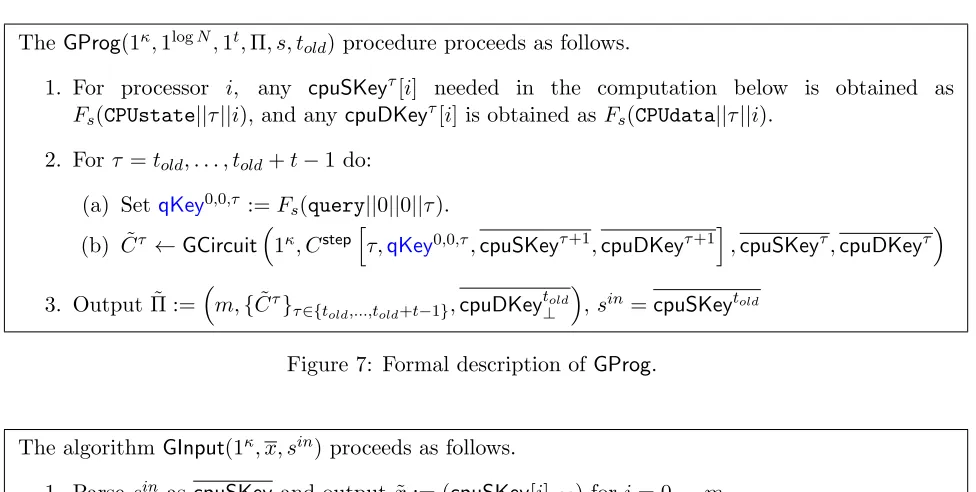
3.4 Program Garbling: ( ˜Π, sin)←GProg(1κ,1logN,1t,Π, s, told)
As we assumed, the program Π is a collision-free OPRAM program. We conceptually identify three distinct steps that are used to compute a parallel CPU step: the main CPU step itself (where each processor takes an input and state, and produces a new state and read/write request), and two types of inter-CPU communication steps that routes the appropriate read/write values before and after memory is accessed. We compile them together as a single large circuit which we describe in Figure 6.
Then each of the t parallel CPU steps are then garbled in sequence as with previous GRAM constructions. We provide the formal garbling of the steps in Figure 7.
3.5 Input Garbling: x˜←GInput(1κ, x, sin)
Input garbling is straightforward: the inputs are treated as selection bits for them-vector of labels. We give a formal description ofGProg in Figure 8.
3.6 Garbled Evaluation: y ←GEvalD˜( ˜Π,x)˜
TheGEvalprocedure gets as input the garbled program ˜Π =told,{C˜τ}τ∈{told,...,told+t−1},cpuDKey
, the garbled input ˜x=cpuSKeyand random access into the garbled database ˜D= ({C˜i,j,k}i∈[d+1],j∈[2i],k∈[K
i],
Cnode[i, k,newLtKey,newRtKey,rKey,qKey]
System parameters: (Will be set to log1M as we will see later.) Hardcoded parameters: [i, k,newLtKey,newRtKey,rKey,qKey]
Input: (rec= (lidx,ridx,oldLKey,oldRKey,tKey),q= (goto,R/W, L, z,cpuDKey)).
Setp:=gotoand p0 := 12 +k.
Setlidx0:=lidxand ridx0:=ridx. SetoldLKey0:=oldLKeyand oldRKey0:=oldRKey.
Defineins(tKey,newLtKey,newRtKey) to be the function that outputstKeywith a possible shift: if 1
2+
(k+ 1)> 12 +k, shifttKeyto the left by 1 and settKey[κ−1] =newLtKey,tKey[2κ−
1] =newRtKey.
We now have three cases:
1. If k < p − 1 then we output (outrKey,outqKey) := (rKeyrec0,qKeyq), where rec0 := (lidx0,ridx0,oldLKey0,oldRKey0,tKey0) wheretKey0 =ins(tKey,newLtKey,newRtKey).
2. Ifk≥p+κ then abort with outputOVERCONSUMPTION-ERROR-I. 3. Ifp−1≤k <p+κthen:
(a) If Li = 0 then,
i. If lidx<p0 then setlidx0 :=p0, goto0 := p0 and oldLKey0 := tKey[0]. Else set lidx0 := lidx+ 1, goto0 := lidx0 and if lidx0 < p0 +κ then set oldLKey0 := tKey[lidx0−p0] else abort withOVERCONSUMPTION-ERROR-II.
ii. SettKey[v] :=⊥for allv <lidx0−p0. SettKey0=ins(tKey,newLtKey,newRtKey). iii. SetoutqKey:=oldLKeyq0, whereq0 :=q but with goto0 replacing goto.
else
i. Ifridx<p0 then set ridx0 :=p0, goto0 :=p0 and oldRKey0 :=tKey[κ]. Else set ridx0 := ridx+ 1, goto0 :=ridx0 and ifridx0 <p0+κ then setoldRKey0 :=tKey[κ+ridx0−p0] else abort withOVERCONSUMPTION-ERROR-II.
ii. SettKey[κ+v] :=⊥for allv <ridx0−p0. SettKey0 =ins(tKey,newLtKey,newRtKey). iii. SetoutqKey:=oldRKeyq0, whereq0:=q but withgoto0 replacinggoto.
(b) Set outrKey := rKeyrec0 where rec0 := (lidx0,ridx0,oldLKey0,oldRKey0,tKey0) and output
(outrKey,outqKey).
Figure 3: Formal description of the nonleaf, thin memory circuit with key passing. This is identical to the node circuit in [7].
Cstep[t,rootqKey,cpuSKey,cpuDKey]
Hardcoded parameters: [t,rootqKey,cpuSKey,cpuDKey] Input: (state,data).
Route the appropriate data to each processor and then compute (state0[i],R/W[i], L[i], z[i]) := CCPUΠ
i(state[i],data[i]) for each processor CPUi. Post-process the queries so that the collision-free property is held, then set q[i] := (R/W[i], L[i], z[i],cpuDKey[i]) and output rootqKeyq and cpuSKey[i]state0[i], or a halt signal.
Cleaf[i, k,dKey,qKey]
System parameters: (Will be set to log1M as we will see later.) Hardcoded parameters: [i, k,dKey,qKey]
Input: (data,q= (goto,R/W, L, z,cpuDKey)).
Setp:=gotoand p0 := 12 +k. We now have three cases:
1. Ifk <p−1 then we output (outdKey,outqKey) := (dKeydata,qKeyq). 2. Ifk≥p+κ then abort with outputOVERCONSUMPTION-ERROR-I.
3. If p −1 ≤ k < p +κ then: If R/W = read then output (dKeydata,cpuDKeydata), else if R/W=writethen output (dKeyz,cpuDKeyz).
Figure 4: Formal description of the leaf Memory Circuit. This is identical to Cleaf[i, k,dKey,qKey] in [7]. See the next page for Figure 5 describing the fullGData algorithm.
TheGProg(1κ,1logN,1t,Π, s, told) procedure proceeds as follows.
1. For processor i, any cpuSKeyτ[i] needed in the computation below is obtained as Fs(CPUstate||τ||i), and anycpuDKeyτ[i] is obtained as Fs(CPUdata||τ||i).
2. Forτ =told, . . . , told+t−1 do:
(a) Set qKey0,0,τ :=Fs(query||0||0||τ).
(b) ˜Cτ ←GCircuit1κ, Cstephτ,qKey0,0,τ,cpuSKeyτ+1,cpuDKeyτ+1i,cpuSKeyτ,cpuDKeyτ
3. Output ˜Π :=
m,{C˜τ}τ∈{told,...,told+t−1},cpuDKey
told ⊥
,sin =cpuSKeytold
Figure 7: Formal description of GProg.
The algorithmGInput(1κ, x, sin) proceeds as follows.
1. Parsesin ascpuSKey and output ˜x:= (cpuSKey[i]x[i]) for i= 0. . . m.
The algorithmGData(1κ, D) proceeds as follows. Without loss of generality we assume thatN = 2d (where N = |D|) where d is a positive integer. Let m the number of parallel memory accesses. We set = log1N. We set and b = log(m)/log(4/3), B = log4N, and γ = log3(N). We set Kb+1 =γN/m, and for each b < i ∈ [d+ 1] and set Ki =
1
2+
Ki−1
+κ. Set W0 = m and
Wi =b(12 +δ)Wi−1c+κ.
1. Lets← {0,1}κ.
2. Any dKeyd,j,k needed in the computation below is obtained as F
s(data||d||j||k). Similarly
for any i, j, k,rKeyi,j,k :=Fs(rec||i||j||k) andqKeyi,j,k:=Fs(query||i||j||k) (truncated to the
correct length, as not all qKeys have the same length). 3. For allb < i < d, j∈[2i], k∈[Ki], set
tKeyi,j,0 := n
qKeyi+1,2j,lo
l∈[κ]
| {z }
left
, nqKeyi+1,2j+1,lo
l∈[κ]
| {z }
right .
and if 1
2 +
(k+ 1) > 1
2 +
(k)
, then set
newLtKeyi,j,k=qKeyi+1,2j,b(12+)(k+1)c+κ−1,newRtKeyi,j,k =qKeyi+1,2j+1,b( 1
2+)(k+1)c+κ−1 , otherwise set newLtKeyi,j,k =newRtKeyi,j,k=⊥.
4. For all i = b, j ∈ [2i], k ∈ [N/m], set tKeyi,j,k = {{qKeyi+1,2j,Bk+l}l∈[B],
{qKeyi+1,2j+1,Bk+l}l∈[B]}.
5. For all 0≤i < b, j ∈[2i], k∈[N/m], settKeyi,j,k={qKeyi+1,2j,k,qKeyi+1,2j+1,k}. 6. For allj∈[2d], k∈[Kd],
˜
Cd,j,k ←GCircuit 1κ,Cleafd, k,dKeyd,j,k+1,qKeyd,j,k+1,dKeyd,j,k,qKeyd,j,k. 7. For allb < i < d, j∈[2i], k∈[Ki],
˜
Ci,j,k ←GCircuit(1κ,Cnodei, k,newLtKeyi,j,k,newRtKeyi,j,k,rKeyi,j,k+1,qKeyi,j,k+1,rKeyi,j,k,
qKeyi,j,k).
8. For alli=b, j ∈[2i], k∈[N/m], ˜Ci,j,k←GCircuit(1κ,Cedgei, k, Wi,tKeyi,j,k
,qKeyi,j,k). 9. For all 0≤i < b, j ∈[2i], k∈[N/m], ˜Ci,j,k←GCircuit(1κ,Cwidei, k, Wi,tKeyi,j,k
,qKeyi,j,k). 10. For all j∈[2d], setTab(d, j) =dKeyd,j,0
D[j].
11. For all b < i ∈ [d], j ∈ [2i], set Tab(i, j) := rKeyi,j,0reci,j,0, where reci,j,0 := (0,0,qKeyi+1,2j,0,qKeyi+1,2j+1,0,tKeyi,j,0).
12. Output ˜D:=
n ˜ Ci,j,ko
i∈[d+1],j∈[2i],k∈[K i]
,{Tab(i, j)}b<i∈[d+1],j∈[2i]
ands.
The algorithmGEvalD˜( ˜Π,x˜) proceeds as follows. 1. Parse ˜Π as told,{C˜τ}τ∈{told,...,told+t−1},cpuDKey
, ˜x ascpuSKey and ˜
D as
n ˜ Ci,j,ko
i∈[d+1],j∈[2i],k∈[K i]
,{Tab(i, j)}i∈[d+1],j∈[2i]
.
2. Forτ ∈ {told, . . . , told+t−1} do:
(a) Evaluate (cpuSKey,qKey0,0,τ) := Eval( ˜Cτ,(cpuSKey,cpuDKey)). If an output y is pro-duced byEval instead, then output y and halt.
(b) Set i= 0, j = 0, k=τ.
(c) For i = 0. . . b − 1, j = 0. . .2i, k = τ, evaluate qKeyi+1,2j,τ,qKeyi+1,2j+1,τ := Eval( ˜Ci,j,k,(qKeyi,j,τ)).
(d) Set B0 =bB(12+δ)c+κ.
(e) For i = b, j = 0. . .2i, k = τ, evaluate
qKeyi+1,2j,B0τ, . . . ,qKeyi+1,2j,B0τ+B0−1,qKeyi+1,2j+1,B0τ, . . . ,qKeyi+1,2j+1,B0τ+B0−1 := Eval( ˜Ci,j,k,(qKeyi,j,τ)).
(f) Fori=b+ 1, j= 0. . .2i, k=B0τ . . . B0τ +B0−1
i. SetqKey=qKeyi,j,k, ifqKey6=⊥, evaluate the subtree as in GLO, i.e. ii. Evaluate outputKey:=Eval( ˜Ci,j,k,(Tab(i, j),qKey)).
A. IfoutputKeyis parsed as (rKey,qKeyi0,j0,k0) for somei0, j0, k0, then setTab(i, j) :=
rKey,qKey:=qKeyi0,j0,k0,(i, j, k) = (i0, j0, k0) and go to Step 2(f)ii.
B. Otherwise, set (dKey,cpuDKey[u]) :=outputKey,andTab(i, j) := dKey, whereu is the appropriate CPU id.
iii. When all subtrees finish evaluating, incrementτ and go to Step 2
Figure 9: Formal description of GEval.
4
Cost and Correctness Analysis
4.1 Overall Cost
In this section, we analyze the cost and correctness of the algorithms above, before delving into the security proof. We work with d = logN, b = log(m)/log(4/3), = log1N,γ = log3N, and B = log4N. First, we observe from the GLO construction, that |Cnode| and |Cleaf| are both poly(logN,logT,logm, κ), and that the CPU step (with the fixed network of inter-CPU communi-cation) is m·poly(logN,logT,logm, κ).
It remains to analyze the size of |Cwide| and |Cedge|. Depending on the level in which these circuits appear, they may be of different sizes. Note, if we letW0 =mandWi=b(21+δ)Wi−1c+κ,
then|Cwide|at leveli is of size (W
i+ 2Wi+1)·poly(logN,logT,logm, κ). We also note|Cedge|has
4.1.1 Cost of GData
The cost of the algorithm GData(1κ, D) is dominated by the cost of garbling each circuit (the table generation is clearly O(N)·poly(logN,logT,logm, κ)). We give a straightforward bound of Kb+1+i ≤ 12+
i
(BN/m+iκ) andWi ≤ 12 +
i
(m+iγ). Recall that we garble enough circuits We must be careful in calculating the cost of the wide circuits, as they cannot be garbled in poly(logN,logT,logm, κ) time, seeing as how their size depends on m. Thus we require a more careful bound, and the cost of garblings of Cnode (ignoring poly(logN,logT,logm, κ) factors) is given as
b
X
i=0
2iN/mWi+ d−1
X
i=b+1
2iKi
≤N/m
b
X
i=0
(1 + 2)i(m+bγ) +
d−b−2
X
i=0
2i+b+1Kb+1+i
≤N/me2b(m+bγ) + 2b+1e2d(BN/m+dκ)
Plugging in the values for d, b, , γ, B, we obtain that this cost isN·poly(logN,logT,logm, κ).
4.1.2 Cost of GProg
The algorithm GProg(1κ,1logN,1t, P, s, told) computes t cpuSKeys,cpuDKeys, and qKeys. It also
garbles t Cstep circuits and outputs them, along with a single cpuSKey. Since each individual operation ism·poly(logN,logT,logm, κ), the overall space cost ispoly(logN,logT,logm, κ)·t·m, though despite the larger space, it can be calculated inm-parallel timepoly(logN,logT,logm, κ)·t.
4.1.3 Cost of GInput
The algorithmGInput(1κ, x, sin) selects labels of the state key based on the state as input. As such,
the space cost ispoly(logN,logT,logm, κ)·m, and again can be prepared in timepoly(logN,logT,logm, κ).
4.1.4 Cost of GEval
For the sake of calculating the cost of GEval, we assume that it does not abort with an error (which, looking ahead, will only occur with negligible probability). At each CPU step, one circuit is evaluated per node above and including level b. At some particular level i < b the circuit is wide and contains O(Wi) gates (but shallow, and hence can be parallelized). From our analysis
above, we know that Pb
i=02iWi ≤ Pbi=0(1 + 2)i(m+bγ) ≤ e2b(m+bγ), and can be evaluated
in poly(logN,logT,logm, κ) time given m parallel processors. For the remainder of the tree, we can think of virtually spawning 2b+1 processes where each process sequentially performs B queries against the subtrees. The query time below level b is calculated from GLO of having amortizedpoly(logN,logT,logm, κ) cost, and therefore incurs 2b+1·B·poly(logN,logT,logm, κ) cost. However, 2b+1 ≤ m and therefore can be parallelized down to poly(logN,logT,logm, κ) overhead.
4.2 Correctness
a negligible probability. Therefore, for correctness, we must show thatKEY-OVERFLOW-ERRORnever occurs except with negligible probability, both atCwide and Cedge.
Claim 4.1. KEY-OVERFLOW-ERRORwith probability negligible in N.
Proof. The only two ways this error is thrown is if a wide circuit of a parent of level i attempts to place more than Wi CPU keys into a child node at level i, or an edge circuit fails the bound
w ≤B. We show that this cannot happen with very high probability. In order to do so, we first put a lower bound onWi and then show that the probability that a particular query will cause a
node at level ito have more than Wi CPU keys is negligible. We have that
Wi= (
1 2+)
im+ i−1
X
j=0
(1 2 +)
jγ ≥ m
2i +
2m 2i +γ
Our goal is to bound the probability that if we pick mrandom leaves that more thanWi paths
from the root to those leaves go through a particular node at level i. Of course, the m random leaves are chosen to be uniformly distinct values, but we can bound this by performing an easier analysis where m are chosen uniformly at random with repetition.
We let X be a variable that indicates the number of paths that take a particular node at level i. We can treatX as a sum ofm independent trials, and thus expect µ= m2i hits on average. We set δ= 2+γµ. Then by the strong form of the Chernoff bound, we have:
P r[X > Wi]≤P r[X >
m 2i +
2m 2i +γ]
≤P r[X > µ(1 +δ)]≤exp
− δ
2µ
2 +δ ≤exp −δµ δ 1 +δ
≤exp
−(2µ+γ)
2+γ/µ 2 + 2+γ/µ
≤exp
−(2µ+γ) 2 3 ≤exp −2 3(2
2µ+γ)
Since γ = loglog3NN, this is negligible inN.
Finally, need to show that Wb ≤B so that Cedge does not cause the error. Here, we use the
upper boundforWb, and assume logN >4. We calculate:
Wb ≤
1 2+
b
(m+bγ)≤
1 2+ 1 4 b
(m+bγ)
≤
3 4
log(m)/log(4/3)
(m+bγ)≤ 1
m(m+bγ)
≤log4N =B
5
UMA2-security Proof
Theorem 5.1 (UMA2-security). Let F be a PRF and(GCircuit,Eval,CircSim)be a circuit garbling scheme, both of which can be built from any one-way function in black-box manner. Then our con-struction (GData,GProg,GInput,GEval) is a UMA2-secure garbled PRAM scheme form-processor uniform parallel access programs running in total time T < N/m making only black-box access to the underlying OWF.
Proof.
Informally, at a high level, we can describe our proof as follows. We know that below level b, the circuits can all be properly simulated due to the fact they are constructed identically to that of GLO (except there are simply more circuits). On the other hand, circuits above this level have no complex parent-to-child wiring, i.e. for each time step, every parent contains exactly the keys for its two children at that time step and not any other time step. Furthermore, circuits within a node above levelbdo not communicate to each other. Thus, simulating these circuits are straightforward: at time steptold, simulate the root circuit ˜C0,0,τ then simulate the next level down ˜C1,0,τ and ˜C1,1,τ
and so forth.
The formal analysis is as follows. Since we are proving UMA2-security, we know ahead of time the number of time steps, the access locations, and hence the exact circuits that will be executed and in which order. Of course, we are evaluating circuits in parallel, but as we shall see, whenever we need to resolve the ordering of two circuits are being executed in parallel, we will already be working in a hybrid in which they are independent of one another, and hence we can arbitrarily assign an order (lexicographically). LetCircSim be the garbled circuit simulator, and letU be the total number of circuits that will be evaluated in the real execution. We show how to construct a simulator Sim and then give a series of hybrids ˆH0, H0, . . . , HU,HˆU such that the first hybrid outputs the ( ˜D,Π˜,x˜) of the is the real execution and the last hybrid is the output of Sim, which we will define. The construction will have a similar structure of previous garbling hybrid schemes, and for the circuits below levelb we use the same analysis as in [7], but still the proof will require new analysis for circuits above level b. H0 is the real execution with the PRF F replaced with a uniform random function (where previously evaluated values are tabulated). Since the PRF key is not used in evaluation, we immediately obtain ˆH0comp≈ H0.
Consider the sequence of circuits that would have been evaluated given MemAccess. This sequence is entirely deterministic and therefore we let S1, . . . , SU be this sequence of circuits, e.g.
S1 = ˜C0(the first parallel CPU step circuit), S2 = ˜C0,0,0(the first root circuit), . . .. Hu simulates
the first u of these circuits, and generates all other circuits as in the real execution. Hybrid Definition: ( ˜D,Π˜,x˜)←Hu
The hybridHuproceeds as follows: For each circuit not inS1, . . . , Su, generate it as you would in
the real execution (note thatGDatacan generate circuits using only, and for each circuitSu, . . . , S1
(in that order) we simulate the circuit using CircSim by giving it as output what it would have generated in the real execution or what was provided as the simulated input labels. Note that this may use information about the database D and the inputs x, and our goal is to show that at the very end,Sim will not need this information.
We now show Hu−1 comp≈ Hu. Either Su is a circuit in the tree, in which case let ibe its level,
or elseSu is a CPU step circuit. We now analyze the possible cases:
1. i= 0 : In a root node, the only circuit that holds its qKeyis the previous step node, which would have already been simulated, so the output ofCircSim is indistinguishable from a real garbling.
from the same time step. Since this was previously evaluated and simulated, we can again simulate this circuit withCircSim.
3. i= b+ 1 : In the level below the edge node, the circuits are arranged as in the root of the GLO construction. However, theqKeyandrKeyinputs for these circuits now can either come from the parent (edge circuit) or a predecessor thin circuit in the same level. These can be handled in batches ofB, sequentially, because every node still has a distinct parent that holds its qKey (that will never be passed on to subsequent parents, as edge circuits do not pass information from one to the next), as well as its immediate predecessor which will already have been simulated. Thus, again we can invokeCircSim.
4. i > b+ 1 : Finally, these nodes all behave as in the GLO construction, and so by the analysis of their construction, these nodes can all also be simulated.
In the final case, ifSu is a CPU step circuit, then only the CPU circuit of the previous time step
has its cpuSKey. On the other hand, itscpuDKeyoriginated from the previous CPU step, but was passed down the entire tree. Due to the way we order the circuits, we ensure that all parallel steps have been completed before this circuit is evaluated, and this ensures that any circuit that passed a cpuDKeyas a value have already been simulated in an earlier hybrid. Thus, any distinguisher of Hu−1 andHu can again be used to distinguish between the output ofCircSimand a real garbling.
After the course of evaluation, there will be of course unevaluated circuits in the final hybrid ˆ
HU. As with [7], we use the same circuit encryption technique (see Appendix B in [8] for a formal proof) and encrypt these circuits so that partial inputs of a garbled circuit reveal nothing about the circuit.
Therefore, our simulator Sim(1κ,1N,1t, y,1D,MemAccess = {Lτ, zread,τ, zwrite,τ}τ=0,...,t−1) can
output the distribution ˆHU without access to D or x. We see this as follows: the simulator,
givenMemAccesscan determine the sequenceS1, . . . , SU. The simulator starts by first replacing all
circuits that won’t be evaluated by replacing them with encryptions of zero. It then simulates the Su in reverse order, starting with simulating SU using the output y, and then working backwards
simulates further ones ensuring that their output is set to the appropriate inputs.
6
Main Theorem
We complete the proof of our main theorem in this section, where we combine our UMA2-secure GPRAM scheme with statistical OPRAM. First, we state a theorem from [3]:
Theorem 6.1(Theorem 3.4 from [3]). There exists an activation-preserving, collision-free OPRAM compiler with polylogarithmic worst-case computational overhead and ω(1) memory overhead.
We make the additional observation that the scheme also produces a uniformly random access pattern that always choosesmrandom memory locations to read from at each step, hence a program compiled under this theorem satisfies the assumption of our UMA2-security theorem. We make the following remark:
Remark on Circuit ReplenishingAs with many previous garbled RAM schemes such as [10,9,
7], the garbled memory eventually becomes consumed and will needed to be refreshed. Our garbled memory is created forN/mtimesteps and for the sake of brevity we refer the reader to [8] for the details of applying such a technique.
Theorem 6.2 (Main Theorem). Assuming the existence of one-way functions, there exists a fully black-box secure garbled PRAM scheme for arbitrary m-processor PRAM programs. The size of the garbled database is O˜(|D|), size of the garbled input is O˜(|x|) and the size of the garbled program is O˜(mT) and its m-parallel evaluation time is O˜(T) where T is the m-parallel running time of programP. HereO˜(·)ignorespoly(logT,log|D|,logm, κ)factors whereκis the security parameter.
Acknowledgments
We thank Alessandra Scafuro for helpful discussions.
References
[1] B. Applebaum, Y. Ishai, and E. Kushilevitz. From secrecy to soundness: Efficient verification via secure computation. In S. Abramsky, C. Gavoille, C. Kirchner, F. Meyer auf der Heide, and P. G. Spirakis, editors,ICALP (1), volume 6198 ofLecture Notes in Computer Science, pages 152–163. Springer, 2010.
[2] N. Bitansky, S. Garg, H. Lin, R. Pass, and S. Telang. Succinct randomized encodings and their ap-plications. In R. A. Servedio and R. Rubinfeld, editors, 47th Annual ACM Symposium on Theory of Computing, pages 439–448, Portland, OR, USA, June 14–17, 2015. ACM Press.
[3] E. Boyle, K.-M. Chung, and R. Pass. Oblivious parallel RAM and applications. Cryptology ePrint Archive, Report 2014/594, 2014. http://eprint.iacr.org/2014/594.
[4] R. Canetti and J. Holmgren. Fully succinct garbled RAM. Cryptology ePrint Archive, Report 2015/388, 2015. http://eprint.iacr.org/2015/388.
[5] R. Canetti, J. Holmgren, A. Jain, and V. Vaikuntanathan. Succinct garbling and indistinguishabil-ity obfuscation for RAM programs. In R. A. Servedio and R. Rubinfeld, editors, 47th Annual ACM Symposium on Theory of Computing, pages 429–437, Portland, OR, USA, June 14–17, 2015. ACM Press.
[6] Y.-C. Chen, S. S. M. Chow, K.-M. Chung, R. W. F. Lai, W.-K. Lin, and H.-S. Zhou. Computation-trace indistinguishability obfuscation and its applications. Cryptology ePrint Archive, Report 2015/406, 2015.
http://eprint.iacr.org/2015/406.
[7] S. Garg, S. Lu, and R. Ostrovsky. Black-box garbled RAM. InAnnual Symposium on Foundations of Computer Science, FOCS 2015, 2015.
[8] S. Garg, S. Lu, and R. Ostrovsky. Black-box garbled RAM. Cryptology ePrint Archive, Report 2015/307, 2015. http://eprint.iacr.org/2015/307.
[9] S. Garg, S. Lu, R. Ostrovsky, and A. Scafuro. Garbled RAM from one-way functions. In R. A. Servedio and R. Rubinfeld, editors, 47th Annual ACM Symposium on Theory of Computing, pages 449–458, Portland, OR, USA, June 14–17, 2015. ACM Press.
[10] C. Gentry, S. Halevi, S. Lu, R. Ostrovsky, M. Raykova, and D. Wichs. Garbled RAM revisited. In P. Q. Nguyen and E. Oswald, editors, Advances in Cryptology – EUROCRYPT 2014, volume 8441 of
Lecture Notes in Computer Science, pages 405–422, Copenhagen, Denmark, May 11–15, 2014. Springer, Heidelberg, Germany.
[11] C. Gentry, S. Halevi, M. Raykova, and D. Wichs. Outsourcing private RAM computation. In55th An-nual Symposium on Foundations of Computer Science, pages 404–413, Philadelphia, PA, USA, Oct. 18– 21, 2014. IEEE Computer Society Press.
[13] O. Goldreich and R. Ostrovsky. Software protection and simulation on oblivious RAMs. J. ACM, 43(3):431–473, 1996.
[14] V. Koppula, A. B. Lewko, and B. Waters. Indistinguishability obfuscation for turing machines with unbounded memory. In R. A. Servedio and R. Rubinfeld, editors, 47th Annual ACM Symposium on Theory of Computing, pages 419–428, Portland, OR, USA, June 14–17, 2015. ACM Press.
[15] S. Lu and R. Ostrovsky. How to garble RAM programs. In T. Johansson and P. Q. Nguyen, editors,
Advances in Cryptology – EUROCRYPT 2013, volume 7881 of Lecture Notes in Computer Science, pages 719–734, Athens, Greece, May 26–30, 2013. Springer, Heidelberg, Germany.
[16] R. Ostrovsky. Efficient computation on oblivious RAMs. In22nd Annual ACM Symposium on Theory of Computing, pages 514–523, Baltimore, Maryland, USA, May 14–16, 1990. ACM Press.
![Figure 3: Formal description of the nonleaf, thin memory circuit with key passing. This is identicalto the node circuit in [7].](https://thumb-us.123doks.com/thumbv2/123dok_us/7921411.1315307/12.612.74.556.82.533/figure-formal-description-nonleaf-circuit-passing-identicalto-circuit.webp)