IJEDR1603032
International Journal of Engineering Development and Research (www.ijedr.org)190
Cascaded Five Level Inverter Switching Sequence
Optimization Using S-Function
1
K. Lavanya Raj,
2N.Karthik
1Student, 2Assistant Professor
1Department Of Electrical & Electronics Engineering 1Bapatla Engineering College,Bapatla,India
________________________________________________________________________________________________________
Abstract - The multilevel inverter utilization has been increased since the last decade. These new type of inverters are suitable in various high voltage and high power applications due to their ability to synthesize waveforms with better harmonic spectrum and faithful output. This paper presents a symmetrical five level cascaded H-bridge multilevel inverter, using multicarrier pulse width modulation technique. And also comparison is made between multicarrier pulse width modulation and the s-function. The Simulation results are presented to prove that THD is reduced with the multicarrier modulation. From the results, the proposed inverter provides higher output quality with relatively lower power loss as compared to the other conventional inverters with the same output quality to compare, the simulation studies have been extended for single phase cascaded H-bridge five level inverter using multi carrier pulse width modulation. The results obtained using S-function are found more reliable compared to multi carrier pulse width modulation, in terms of total harmonic distortion. The system was simulated using Mat lab/Simulink.
Index Terms - Cascaded H-bridge multilevel inverter (CH-MLI), S-function, multicarrier pulse-width modulation, total harmonic distortion (THD).
________________________________________________________________________________________________________
I.INTRODUCTION
The concept of multilevel inverters has been introduced since 1975.The term multilevel began with the three-level converter. Subsequently, several multilevel inverter topologies have been developed. Multilevel inverters (MLIs) produce a desired output voltage from several levels of DC voltages as inputs. By taking sufficient number of DC sources, a nearly sinusoidal voltage waveform can be obtained. Capacitors, batteries, and renewable energy voltage sources can be used as the multiple dc voltage sources.
Multilevel inverters include an array of power semiconductors and capacitor voltage sources, the output of which generate voltages with stepped waveforms. The commutation of the power switches aggregate these multiple dc sources in order to achieve high voltage at the output; however, the rated voltage of the power semiconductor switches depends only upon the rating of the dc voltage sources to which they are connected. A multilevel converter can switch either its input or output nodes (or both) between multiple (more than two) levels of voltage or current. As the number of levels reaches infinity, the output THD approaches zero. The number of the achievable voltage levels, however, is limited by voltage-imbalance problems, voltage clamping requirements, circuit layout and packaging constraints complexity of the controller, and, of course, capital and maintenance costs. The most attractive features of multilevel inverters are as follows:-
1) They can generate output voltages with extremely low distortion and lower dv/dt. 2) They draw input current with very low distortion.
3) They generate smaller common mode (CM) voltage, thus reducing the stress in the motor bearings. In addition, using sophisticated modulation methods, CM voltages can be eliminated.
4) They can operate with a lower switching frequency.
To control the output voltage and reduce undesired harmonics, multi carrier pulse width modulation techniques, wherein specific higher order harmonics such as 5th, 7th, 11th and 13th are suppressed in the output voltage of the inverter. Modularity also permits the cascaded multilevel inverter to be stacked easily for high power and high-voltage applications.
The multilevel inverter has been implemented in various applications ranging from medium to high-power levels, such as motor drives, power conditioning devices, also conventional or renewable energy generation and distribution. The different multilevel inverter structures are cascaded H-bridge, diode clamped and flying capacitor multilevel inverter.
IJEDR1603032
International Journal of Engineering Development and Research (www.ijedr.org)191
II.CASCADEDH-BRIDGEMULTILEVELINVERTERCascaded H-Bridge (CHB) configuration has recently become very popular in high-power AC supplies and adjustable-speed drive applications. A cascade multilevel inverter consists of a series of H-bridge (single-phase full bridge) inverter units in each of its three phases. Each H-bridge unit has its own dc source, which for an induction motor would be a battery unit, fuel cell or solar cell. Each SDC (separate D.C. source) is associated with a single-phase full-bridge inverter. The ac terminal voltages of different level inverters are connected in series Each H- bridge unit generates a quasi-square waveform by phase shifting its positive and negative phase legs‟ switching timings. Each switching device always conducts for 180° (or half cycle) regardless of the pulse width of the quasi-square wave. This switching method makes all of the switching devices current stress equal.
In the motoring mode, power flows from the batteries through the cascade inverters to the motor. In the charging mode, the cascade converters act as rectifiers, and power flows from the charger (ac source) to the batteries. The cascade converters can also act as rectifiers to help recover the kinetic energy of the vehicle if regenerative braking is used.
The basic circuit of a single-phase m-level CH-MLI is shown in Fig1. It consists of (m-1)/2 cells connected in series in each phase. Each cell consists of single-phase H-bridge inverter with separate DC source. There are four active devices in each cell and a cell can produce three voltage levels 0, Vdc/2 and _Vdc/2. When switches S1 and S2 of one H-bridge inverter are closed, the output voltage is -Vdc/2 and when switches S3 and S4 are closed, the output voltage are +Vdc/2. When either the switches S1 and S3 or the switches S4 and S2 are closed, the output voltage is 0. Higher output voltage levels can be obtained by connecting these cells in cascade. The phase voltage Van in a CH-MLI is the sum of voltages of individual cells.
Van(t) = V1(t)+V2(t)+....+VM(t)
The cascaded H-bridge multilevel inverters have been applied where high power and power quality are essential, for example, static synchronous compensators, active filter and reactive power compensation applications, photo voltaic power conversion, uninterruptible power supplies, and magnetic resonance imaging. Furthermore, one of the growing applications for multilevel motor drive is electric and hybrid power trains.
In this topology, each cell has separate dc link capacitor and the voltage across the capacitor might differ among the cells. So, each power circuit needs just one dc voltage source. The number of dc link capacitors is proportional to the number of phase voltage levels .Each bridge cell may have positive, negative or zero voltage. Final output voltage is the sum of all H-bridge cell voltages and is symmetric with respect to neutral point, so the number of voltage levels is odd. Cascaded H-H-bridge multilevel inverters typically use IGBT switches. These switches have low block voltage and high switching frequency.
Fig 1- Single-phase m-level CH-MLI Fig 2- Output voltage waveform of CH-MLI.
IJEDR1603032
International Journal of Engineering Development and Research (www.ijedr.org)192
In this topology, for generating the switching pulses multicarrier phase shifted pulse width modulation and embedded mat lab S-function are used. In the multicarrier modulation, the amplitude and frequency of all triangular carriers are the same as well as the phase shifts between adjacent carriers.PWM signals are pulse trains with fixed frequency and magnitude and variable pulse width. There is one pulse of fixed magnitude in every PWM period. However, the width of the pulses changes from pulse to pulse according to a modulating signal. When a PWM signal is applied to the gate of a power transistor, it causes the turn on and turns off intervals of the transistor to change from one PWM period to another PWM period according to the same modulating signal. The advantages possessed by PWM techniques are Lower power dissipation, Easy to implement and control, No temperature variation and aging-caused drifting or degradation in linearity, Compatible with today’s digital micro-processors, the output voltage control can be obtained without any additional components and with the method, lower order harmonics can be eliminated or minimized along with its output voltage control. As higher order harmonics can be filtered easily, the filtering requirements are minimized.
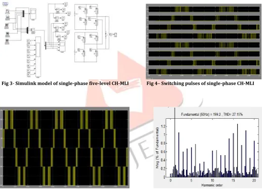
Fig 3- Simulink model of single-phase five-level CH-MLI Fig 4– Switching pulses of single-phase CH-MLI
Fig 5- Line voltages of single-phase CH-MLI using MCPWM Fig 6-Harmonic spectrum of line voltage using MCPWM
IJEDR1603032
International Journal of Engineering Development and Research (www.ijedr.org)193
Fig- 7: Simulink model of single-phase five-level CH-MLI
using S-function Fig-8: Sub-circuit of pulse generation block using s-function
Fig-9:Switching pulses of single-phase CH-MLI
using S-function Fig-10: Line voltages of single-phase CH-MLI
using S- function
Fig-11: Harmonic spectrum of line voltage using S-function
SIMULATION STUDIES
IJEDR1603032
International Journal of Engineering Development and Research (www.ijedr.org)194
A sub-circuit block designed to generate switching pulses for single-phase, five-level CH-MLI using S-function is shown in Fig.8. The switching pulses are generated for the switches of single-phase, five-level CH-MLI on the basis of a program written in MATLAB.The switching pulses generated using S-function is shown in Fig.9. Switching pulse with magnitude ‘1’ indicates that the switch is ‘on’ and the magnitude ‘0’ indicates that the switch is ‘off’. Similarly switching pulses for other phases are also generated. These switching pulses are used for turning ‘on’ and ‘off’ the switches of CH-MLI. Fig.10. shows the line voltage of single-phase, five-level cascaded CH-MLI and Fig.11.shows the harmonic spectrum of one of the line voltages using S-function. It is evident from the harmonic spectrum that the lower order harmonics reduce significantly. The total harmonic distortion (THD)is found to be 21.82%.
SINGLE-PHASE CH-MLI USING MCPWM
To compare the results of single-phase, five-level CH-MLI using S-function, the single-phase, five-level CH-MLI has been simulated using one of the widely used PWM techniques, MCPWM. Fig.3. shows the sub-circuit of single-phase, five-level CH-MLI using MCPWM. The line voltages of single-phase, five-level cascaded CH-CH-MLI is shown in Fig.5. and the harmonic spectrum of one of the line voltages using MCPWM is shown in Fig. 6. The THD is 27.15%.
IV.CONCLUSION
In this paper, a five level cascaded H-bridge multilevel with multicarrier pulse width modulation and embedded mat lab S- function, is presented. The simulation results show that the total harmonic distortion is low for multicarrier modulation method. The total harmonic distortion can be further reduced by using S-function circuit. This circuit also reduces the number of switches and sources.
REFERENCES
[1] Vivek Kumar Gupta, R. Mahanty Optimized switching scheme of cascaded H-bridge multilevel inverter using PSO- www.elsevier.com/locate/ijepes
2] Lai JS, Peng FZ. Multilevel converters—a new breed of power converters. IEEE Trans Ind Appl 1996; 32(3):509–17.
[3] Rodr´ıguez J, Lai J, Peng FZ. Multilevel inverters: a survey of topologies, controls and applications. IEEE Trans Ind Electron 2002; 49(4):724–38.
[4] Tolbert LM, Peng FZ, Habetler TG. Multilevel converter for large electric drives. IEEE Trans Ind Appl 1999; 35(1):36–44. [5] Gupta R, Ghosh A, Joshi A. Control of cascaded transformer multilevel inverter based DSTATCOM. Elect Power Syst Res 2007; 77(8):989–99.
[6] Patnaik SS, Panda AK. Three-level H-bridge and three H-briges-based three phase four-wire shunt active power filter topologies for high voltage applications. Int J Electr Power Energy Syst 2013; 51:298–306.
[7] Dahidah MSA, Agelidis VG. Single-carrier sinusoidal PWM-equivalent selective harmonic elimination for a five-level voltage source converter. Elect Power Syst Res 2008; 78(11):1826–36.
[8] Kouro S, Rebolledo J, Rodriguez J. Reduced switching-frequency modulation algorithm for high-power multilevel inverters. IEEE Trans Ind Electron 2007; 54(5):2894–901.
[9] Marzoughi A, Imaneini H, Moeini A. An optimal selective harmonic mitigation technique for high power converters. Int J Electr Power Energy Syst 2013; 49:34–9.
[10] Patel HS, Hoft RG. Generalized harmonic elimination and voltage control in thyristor inverters: part I—harmonic elimination. IEEE Trans Ind Appl 1973; 9(3):310–7.
[11] Patel HS, Hoft RG. Generalized harmonic elimination and voltage control in thyristor inverters: part II—voltage control technique. IEEE Trans Ind Appl 1974; 10(5):666–73.