Half adder capabilities of a coupled quantum dot device
P. Pfeffer,1 F. Hartmann,1 I. Neri,2 A. Schade,1 M. Emmerling,1 M. Kamp,1 L. Gammaitoni,2 S. H¨ofling,1, 3 and L. Worschech1
1)Technische Physik and Wilhelm Conrad R¨ontgen Research
Center for Complex Material Systems, Physikalisches Institut,
Universit¨at W¨urzburg, Am Hubland, D-97074 W¨urzburg,
Germany
2)NiPS Laboratory, Dipartimento di Fisica e Geologia, Universit`a di Perugia,
I-06123 Perugia, Italy
3)SUPA, School of Physics and Astronomy, University of St Andrews, St Andrews,
KY16 9SS, United Kingdom
(Dated: 25 January 2016)
ABSTRACT
In this paper we demonstrate two realizations of a half adder based on a voltage-rectifying mechanism involving two Coulomb-coupled quantum dots. First, we examine the ranges of
operation of the half adder’s individual elements, the AND and XOR gates, for a single rectifying device. It allows a switching between the two gates by a control voltage and thus enables a clocked half adder operation. The logic gates are shown to be reliably operative
in a broad noise amplitude range with negligible error probabilities. Subsequently, we study the implementation of the half adder in a combined double-device consisting of two individually tunable rectifiers. We show that this double device allows a simultaneous
operation of both relevant gates at once. The presented devices draw their power solely from electronic fluctuations and are therefore an advancement in the field of energy
1. INTRODUCTION
Making use of surplus noise and heat has become a major focus of research situated at the intersection between physics and engineering1–3. While the related basic research con-centrates on the discovery and exploration of new beneficial concepts and mechanisms such as brownian motors, phonon rectifiers, SQUID ratchets or piezoelectric nanogenerators4–14 more application-near engineering turns its attention to the elaboration of self-powered
and sustainable electronic devices15–19. Recently, we demonstrated voltage rectification and logical stochastic resonance in a semiconductor system based on Coulomb-coupled quantum cavities20,21. Here, we explore this system’s capability to be configured and utilized as a half adder.
A half adder is an electronic circuit which is able to add up two binary digits x and
y. It provides the two outputs sum (s) and carry (c). The half adder is one of the most elementary building blocks of electronic circuits which finds its use in more complex logic elements like full adders, multibit adders or arithmetic logic units22. The half adder can be realized by various interconnections of logic gates, for instance by a combination of several AND, OR, NAND and NOR gates or alternatively of five NAND gates or of five NOR gates. The most compact form, however, is a design which uses only one AND and one XOR gate.
In this case, each gate is fed with the two inputs x and y. The XOR gate produces the output s, the AND gate the outputc22.
In this research, we examined two different devices named ”single device” and ”double device”. Both devices are made up of modulation-doped GaAs/(Al,Ga)As heterostructures including a two-dimensional electron gas situated 80 nm below the surface. The devices
were fabricated via molecular beam epitaxy and structured employing electron beam lithog-raphy and dry chemical etching methods. Whereas the single device has smaller dimensions
compared with the double device, it requires a working in two sequential steps. The double device, on the other hand, allows a time independent, simultaneous output of both the sum and the carry bits. Both devices operate using electronic noise as power source and gate
Vl (V) 0 0 0.6 0.6
Vr (V) 0 0.6 0 0.6
Input 0 1 1 2
AND 0 0 0 1
XOR 0 1 1 0
TABLE I. Definition of the variableInput and logic truth table including AND and XOR (low: 0,
high: 1) with respect to the logic input voltages which either take the high level 0.6 V or the low
level 0 V.
2. DEVICE OPERATION
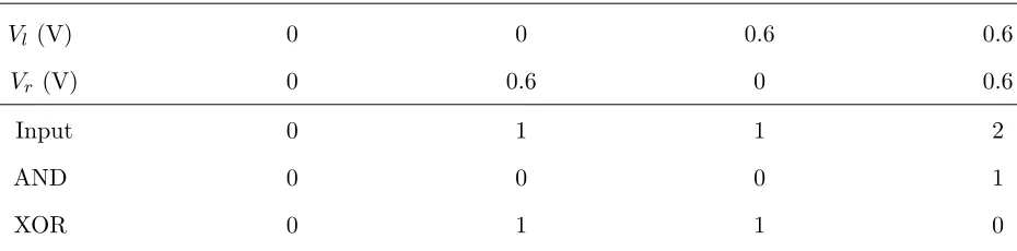
Figure 1(a) shows an electron microscopy image of the single device which features two Coulomb-coupled quantum dots QDt and QDb which are coupled via quantum point
con-tacts (QPCs) to two leads (blue shaded region) and a single reservoir (red shaded region), respectively. Two side gates (green regions) can be used to influence the conductances of the upper QPCs. Tuning these QPCs to an asymmetric configuration and applying a noise
voltageVnoise(t) to the lower reservoir causes a current flow through the upper leads. To pro-vide the noise voltage, a source with Gaussian-distributed, spectrally flat noise output with a cut-off frequency f=20 MHz and a root mean square noise amplitude σnoise was employed.
For an extended description of the basic operational details and theoretical backgrounds see references [20] and [21] as well as [10] and [11].
In order to realize logic gates, the voltages applied to the sidegates, Vl and Vr, are con-sidered as logical inputs and the output current I as logical output. Throughout this work, the values for high and low input voltages are defined to be 0.6 V and 0 V, respectively.
To simplify the notation, we introduce the parameter Input which represents the side gate voltage configurations according to Table 1. Table 1 also includes the truth table for the
relevant AND and XOR gates.
On a similar sample, we were in a recent publication able to demonstrate OR, NOR, AND and NAND gate functionalities which can be switched between, varying the root
[image:3.612.73.538.73.188.2]AND, V = -3.0 V
gbXOR, V = -2.70 V
gb0 5 10 15
0 5 10 15 20 I (nA) time (s)
0 5 10 15
I Input 20 25 0 1 2 Input
d)
500 nm QDt QDbV +V
gb noise(t)
V
lV
rI
a)
b)
time Vgb -3.0 -2.7 time Input 2 1 0c)
-4.0 -3.5 -3.0 -2.5 -2.0 -1.5 0 5 10 15 20 AND
Input = 0 Input = 1 Input = 2
I
(n
A
)
V
gb(V)
NOR XOR
AND XOR AND XOR AND
FIG. 1. (a) Electron microscopy image of the single device with attached circuit diagram. A
currentI flows through the upper part of the device (blue) when electronic fluctuations (Vnoise(t))
are applied to the lower part (red). Logic input voltages Vl and Vr can be applied to the upper
side gates (green) and enable a logic functioning of the device. (b) Simulation of the output
current depending onVgb. The yellow shaded region shows the range where an AND gate is to be
expected, the green region the XOR gate range, and the blue region the NOR gate range. Details
can be found in the main text. (c) Graphical explanation of the measurement scheme used in (d).
Vgb is switched between -2.7 and -3.0 V in order to alternate the system’s logical characteristic
between AND and XOR. While an AND or XOR functionality is established, theInputparameter
is switched between 0, 1 and 2. (d) Time-dependent measurements of the output currents for
switching input levels and sσnoise= 35.25 mV. The black lines designate the thresholdIth between
[image:4.612.74.529.72.464.2]mentioned gate functionalities, particularly the AND functionality, and moreover the XOR
functionality, which are necessary for the compact half adder. All experiments reported here were performed in the dark at 4.2 K by immersing the samples in liquid helium.
3. RESULTS AND DISCUSSION - SINGLE DEVICE
We simulated the system’s dependence on Vgb and on the input parameters according to the modelling in reference [21]. The following model parameters were used: c= 0.014, ηl,l = 3.78×10⁻³, ηl,r = 2.44×10⁻³, ηr,r = 2.84×10⁻³, ηr,l = 2.40×10⁻³, η0 = 2.4×10⁻⁴, E0,l = 7.0×10⁻³ eV, E
0,r = 5.3×10⁻³ eV and σnoise = 35.25 mV. The results are displayed in Figure 1(b). Going from lower to higher Vgb, the current traces for the individual input
configurations successively cross the current threshold, so that AND, XOR and NOR gate functionalities can be obtained. According to the simulation, the AND gate can be found in
the Vgb voltage range from -3.27 to -2.97 V, the XOR gate between -2.73 and -2.43 V and the NOR gate between -2.18 and -1.88 V.
Time-dependent current traces during a switching of the input voltages can be seen in
Figure 1(d), the switching scheme is graphically explained in Figure 1(c). We set the thresh-old Ith between high and low output currents to a value of 15 nA. For σnoise = 35.25 mV
Vgb = −3.00 V leads to an AND gate and Vgb = −2.70 V to an XOR gate. Consequently,
changing of Vgb between these two values switches the device’s output between the carry and sum bits. The possibility to switch between the gates allows the implementation of a
sequential half adder, working in a two-step cycle and requiring a clocking ofVgb. Moreover, programmable, multi-function logic gates offer the possibility to realize software based com-puting architectures which entail the chance to improve comcom-puting efficiency and speed, for
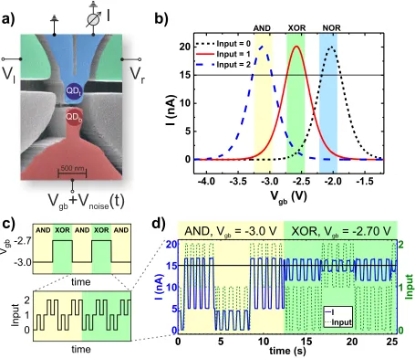
instance by adapting the logic network ideally to specific problems and upcoming calculations or by facilitating approximate computing schemes23–25. Furthermore, reconfigurable archi-tectures allow functional upgrades, ameliorations and rearrangements during their lifecycle26. In order to determine the range of σnoise in which an operation of the AND and XOR gates are possible, we measured the particular output currents for different σnoise. The
re-sults are presented in Figure 2(a) and (b), respectively. The current rises with increasing
threshold. Correspondingly, the XOR gate is available when only the Input = 1 output
values are above threshold. The green regions indicate the σnoise range where an operation of both gates and thus of the half adder is possible. Figure 2(c) shows the probabilities
of erroneous switchings for the individual gates with Ith = 15 nA. The probabilities were calculated from approx. 2000 switchings for each noise value. The σnoise ranges for low error probabilities coincide largely with the operational ranges from Figure 2(a) and(b). In
a narrower interval, the system reaches error probabilities close to zero. The optimal scope for the implementation of a sequential half adder is hence for Ith = 15 nA between approx.
33.8 and 35.3 mV.
In principle, if Ith is set to lower values, smaller σnoise can be used as well. Tests of the device at lower noise amplitudes revealed error probabilities of about 0.4 % for σnoise = 9
and 15 mV using XOR and AND gate configurations. Only if σnoise is further lowered, the error probabilities increase significantly. For those evaluations, the threshold current was chosen to yield best results. The low noise error probabilities are presented in Figure 2(d).
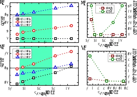
Using the same parameters as for the simulation in Figure 1(b), we can model the output current’s dependence onσnoise. As Figure 3 shows, the output currents as well as the
differ-ence between the individual curves increase with increasing noise amplitude. Consequently, higher output powers and higher signal to noise ratios are expected for higher σnoise. Figure 3(a) presents the AND gate simulation, Figure 3(b) the XOR gate simulation. For the AND
gate, it is desired, that the Input = 2 curve features significantly higher currents than the other curves. For the XOR gate, the Input = 1 currents need to be higher than the other
ones.
Since the device converts the noise into useful energy, we can calculate the highest input switching frequency at which the converted energy still exceeds the energy needed to switch
the logic functionality. The maximal switching frequency at which the converted energy just equals the energy dissipated on a single side gate (E = 1/2 CV2, V = 0.6 V) depends on the output power’s magnitude and thus on the noise amplitude. In order to evaluate the
maximal gate switching frequency for the measurements done at σnoise= 35.25 mV (Figure 1(d) ), we estimate the side gate - channel capacitance C from Coulomb-diamond
32 34 36 38 40 10 15 20 0 5 10 15 20
32 34 36 38 40
0 10 20 30 40 50
Input = 0 Input = 1 Input = 2
s
noise (mV)
I
(n
A
)
Input = 0 Input = 1 Input = 2
I (n A )
c)
b)
E rr o r P ro b a b il it y (% ) snoise (mV)
AND XOR
a)
2 4 6 8 10 12 14 16
0 2 4 6 8 10
d)
AND XOR E rr o r P ro b a b il it y (% ) snoise (mV)
FIG. 2. (a), (b) Output currents for the different Input values in dependence on σnoise. The
green areas show the region, where an AND gate (a) and an XOR gate (b) is established, the
black line designates the output threshold. (a) Vgb = −3.00 V. (b) Vgb = −2.70 V. (c) Error
probabilities versus σnoise for Vgb = −3.00 V (AND) and Vgb = −2.70 V (XOR). Ith = 15 nA.
(d) Error probabilities for lower noise amplitudes. Ith is set to the values yielding the lowest error
probability for each σnoise individually. The dotted lines are guides for the eye.
side-area of the gate next to the channel A ≈6×10⁻¹⁴ m2 (about 30 nm width and 2 µm length). The estimations yield 0.27 aF and 23 aF for the Coulomb-diamond and geometrical considerations, respectively. Assuming that the system spends equal amounts of time in
the different output states defined by the input configurations, we calculate a mean output current of Imean = 10 nA. According to reference [20] the device provides an output power of approx. 3 pW at this output current. From this, we calculate the maximal switching
[image:7.612.77.529.74.395.2]0
10
20
30
40
50
60
0
10
20
30
40
50
0
10
20
30
40
50
60
0
10
20
30
40
50
b
)
Input = 0 Input = 1 Input = 2
s
noise (mV)
I (nA)
Input = 0 Input = 1 Input = 2
a
)
s
noise (mV)
[image:8.612.75.539.77.319.2]I (nA)
FIG. 3. Simulation of the output current depending on σnoise for Input = 0, 1 and 2. a) AND
gate,Vgb =−3.0 V, b) XOR gate,Vgb=−2.7 V. The simulations in (a) and (b) correspond to the experiments shown in Fig. 2 (a) and (b) respectively.
of the side gate - channel capacitance is smaller than the energy generated by the device which theoretically allows an operation which solely relies on the noise floor as power source. In contrast to a conventional logic gate, output currents which are larger than zero for the
low output states are advantageous in our device, since higher output currents mean a higher output power which theoretically allows higher switching frequencies.
4. RESULTS AND DISCUSSION - DOUBLE DEVICE
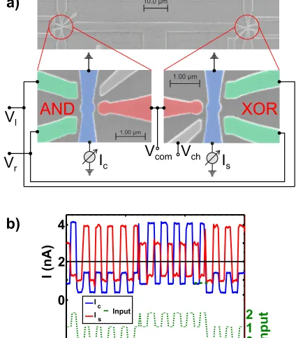
Aiming for a simultaneous operation of the half adder in a single device, we fabricated
the double device which is shown in Figure 4(a). The upper part of the figure displays an electron microscopy image of the main structured area whereas the lower part zooms into the sample’s two functional regions. These two parts are connected by a common noise
I
c
I
s
V
r
V
l
V
com
V
ch
AND
XOR
10.0 µm
1.00 µm
1.00 µm
a)
b)
0
5
10
15
0
2
4
I (nA)
t (s)
0
5
10
15
0
1
2
Input
I
c
I
s
Input
FIG. 4. (a) Electron microscopy image of the double device with attached circuit diagram. The
double device consists of two individual rectifiers which have a common contact with the applied
voltage Vcom=Vgb+Vnoise(t). Additionally, Vch can influence the conductance of solely the right
channel. (b) Time-dependent measurement of the output currents Ic and Is for switching input
[image:9.612.91.515.80.563.2]a single reservoir (where Vcom is applied and which is connected to a quantum dot, red),
of a second quantum dot (which is capacitively coupled to the first one and connected to two leads, blue), and of two side gates (which influence the second quantum dots QPCs,
green). Since Vgb now affects both functional regions at the same time, the right region is furthermore equipped with a supplementary gate where the voltage Vch has an additional effect on the right channel’s conductance. Figure 4(a) moreover displays the equivalent
circuit of the half adder where Vl and Vr are both applied to the left and right side gates simultaneously. Icrepresents the half adder’s carry signal andIsthe half adder’s sum signal.
Similar to the single device, the logical functionalities of the double device can be ma-nipulated to obtain several different gates varying Vcom, i.e. Vgb and σnoise. In order to change both subdevices’ functionalities independently, Vch needs to be employed as well.
However, a purposeful unequal fabrication of the double device’s two parts could be used to intrinsically tune one part to the AND and the other part to the XOR functionality. In this case, Vgb and Vch would no longer be necessary for a half adder operation. For the
measurement with the present sample in Figure 4(b), where the output currents are plotted versus time for switching input voltages, the control voltages were tuned to Vgb = −1.8 V
and Vch =−0.7 V, so that Ic produces the logical characteristics of an AND, Is of an XOR gate. Consequently, the device is a realization of a half adder which adds up the binary values represented by Vl and Vr and produces the output signals sumIs and carryIc.
Analogous to the single device, we estimate the capacitance between a side gate and the current carrying channel from geometrical considerations and thereby assess a maximal
switching frequency at which the energy conversion just outweighs the energy dissipated during a side gate charging. The calculations yield a capacitance of 0.44 aF (d=120 nm, A=10 nm×600 nm = 6×10⁻¹⁵ m2), a mean output current ofI
mean= 2 nA, a mean output power of Pmean = 0.2 pW and a switching frequency of approx. 0.25 MHz which is smaller than the values estimated with the single device. This is due to the lower output currents and output powers which result from a lower capacitive coupling between the two quantum
5. CONCLUSION
In summary, we introduced a nanoscale half adder powered by electronic fluctuations.
We examined the characteristics and working ranges of our voltage rectifier tuned with a control voltage to provide AND and XOR gate functionalities. A reliable functioning of both gates is shown to be possible starting from noise magnitudes as low as 9 mV. The
controllable switching between the gates allows a sequential, clocked operation, having as advantage the small size of the logic element. Moreover, we demonstrated the integration of two individually rectifying structures into a single device, making possible the realization
of a time-independent, combinational logic half adder working solely by means of voltage rectification and noise exploitation. Lastly, we assessed the maximal switching frequency at
which the generated energy just equals the energy needed for a switching operation. This frequency was found to be between 0.72 and 62 MHz for the single device and to be around 0.25 MHz for the double device.
This work presents a proof of concept. Next steps towards a fully employable device would involve research tackling the efficiency of the device and aiming for an increase of the output/input voltage ratio. Furthermore, it is conceivable to customize the design of
the rectifying elements so as to avoid the application of the control voltages Vgb and Vch and to allow a direct operation of the desired logic gate. Our findings are advances on the
way leading to autonomous and energy-efficient electronics which could rely solely on excess electronic fluctuations, waste heat or thermal gradients.
ACKNOWLEDGEMENTS
We gratefully acknowledge financial support from the European Union (FPVII,
REFERENCES
1E. Pop, “Energy dissipation and transport in nanoscale devices,” Nano Res. 3, 147–169
(2010).
2Z. L. Wang and W. Wu, “Nanotechnology-enabled energy harvesting for self-powered
micro-/nanosystems,” Angew. Chem. Int. Ed. 51, 11700–11721 (2012).
3L. Gammaitoni, “There’s plenty of energy at the bottom (micro and nano scale nonlinear
noise harvesting),” Contemporary Physics53, 119–135 (2012).
4R. D. Astumian and P. Hanggi, “Brownian motors,” Phys. Today 55, 33–39 (2002). 5Z. L. Wang and J. Song, “Piezoelectric nanogenerators based on zinc oxide nanowire
arrays,” Science312, 242–246 (2006).
6N. Zeng and J.-S. Wang, “Mechanisms causing thermal rectification: The influence of
phonon frequency, asymmetry, and nonlinear interactions,” Phys. Rev. B 78, 024305 (2008).
7Y. Qin, X. Wang, and Z. L. Wang, “Microfibre–nanowire hybrid structure for energy
scavenging,” Nature 451, 809–813 (2008).
8A. Sterck, D. Koelle, and R. Kleiner, “Rectification in a stochastically driven
three-junction squid rocking ratchet,” Phys. Rev. Lett. 103, 047001 (2009).
9S. Xu, B. J. Hansen, and Z. L. Wang, “Piezoelectric-nanowire-enabled power source for
driving wireless microelectronics,” Nature communications1, 93 (2010).
10R. S´anchez and M. B¨uttiker, “Optimal energy quanta to current conversion,” Phys. Rev.
B 83, 085428 (2011).
11B. Sothmann, R. S´anchez, A. N. Jordan, and M. B¨uttiker, “Rectification of thermal
fluctuations in a chaotic cavity heat engine,” Phys. Rev. B 85, 205301 (2012).
12A. Gnoli, A. Petri, F. Dalton, G. Pontuale, G. Gradenigo, A. Sarracino, and A. Puglisi,
“Brownian ratchet in a thermal bath driven by coulomb friction,” Phys. Rev. Lett. 110, 120601 (2013).
13M. L´opez-Su´arez, G. Abadal, L. Gammaitoni, and R. Rurali, “Noise energy harvesting in
buckled{BN}nanoribbons from molecular dynamics,” Nano Energy15, 329 – 334 (2015). 14B. Sothmann, R. S´anchez, and A. N. Jordan, “Thermoelectric energy harvesting with
15M. Lallart and D. Guyomar, “An optimized self-powered switching circuit for non-linear
energy harvesting with low voltage output,” Smart Materials and Structures 17, 035030 (2008).
16V. Leonov and R. J. Vullers, “Wearable electronics self-powered by using human body
heat: The state of the art and the perspective,” Journal of Renewable and Sustainable Energy 1, 062701 (2009).
17P.-P. Chao, “Energy harvesting electronics for vibratory devices in self-powered sensors,”
Sensors Journal, IEEE 11, 3106–3121 (2011).
18Z. L. Wang, “Self-powered nanosensors and nanosystems,” Adv. Mater. 24, 280–285
(2012).
19V. Misra, A. Bozkurt, B. Calhoun, T. Jackson, J. Jur, J. Lach, B. Lee, J. Muth, O. Oralkan,
M. Ozturk, S. Trolier-McKinstry, D. Vashaee, D. Wentzloff, and Y. Zhu, “Flexible tech-nologies for self-powered wearable health and environmental sensing,” Proceedings of the IEEE 103, 665–681 (2015).
20F. Hartmann, P. Pfeffer, S. H¨ofling, M. Kamp, and L. Worschech, “Voltage fluctuation
to current converter with coulomb-coupled quantum dots,” Phys. Rev. Lett. 114, 146805
(2015).
21P. Pfeffer, F. Hartmann, S. H¨ofling, M. Kamp, and L. Worschech, “Logical stochastic
resonance with a coulomb-coupled quantum-dot rectifier,” Phys. Rev. Applied 4, 014011
(2015).
22D. Page, A Practical Introduction to Computer Architecture, Texts in Computer Science
(Springer, 2009).
23K. Compton and S. Hauck, “Reconfigurable computing: a survey of systems and software,”
ACM Comput. Surv. 34, 171–210 (2002).
24A. Ney, C. Pampuch, R. Koch, and K. Ploog, “Programmable computing with a single
magnetoresistive element,” Nature 425, 485–487 (2003).
25S. Venkataramani, S. T. Chakradhar, K. Roy, and A. Raghunathan, “Approximate
com-puting and the quest for comcom-puting efficiency,” inProceedings of the 52Nd Annual Design
Automation Conference, DAC ’15 (ACM, New York, NY, USA, 2015) pp. 120:1–120:6.
26R. Tessier, K. Pocek, and A. DeHon, “Reconfigurable computing architectures,”