Direct Repetitive Control with Gain Scheduling
Feature for Stand-Alone Generating Applications
A. Lidozzi, L. Solero, F. Crescimbini C. Ji, P. Zanchetta
ROMA TRE University, Dept. of Engineering C-PED, Center for Power Electronics and Drives
Via della Vasca Navale 79, 00146 Roma (Italy) email: [email protected]
Dept. of Electrical and Electronic Engineering University of Nottingham, UK
email: [email protected]
Abstract—This paper deals with the gain scheduling feature for zero-phase-shift direct repetitive control (dRC) implemented in a FPGA system. Proposed control structure is intended to be used in ultra-low THD, fast transient response stand-alone generating applications. Moreover, implementation aspects of the dRC and gain scheduling algorithm are highlighted with reference to an industrial-grade μProcessor-FPGA control system and its graphical programming capabilities.
Keywords—Repetitive control, gain scheduling, stand-alone applications, FPGA target, LabVIEW, Real-Time target.
I. INTRODUCTION
The reduction of the harmonic content of current and voltage waveforms at the output of power electronic converters is of increasing interest for today's applications, with particular reference to either Distributed Generation Systems or Uninterruptible Power Supplies or active filtering, which have to comply with severe Standards. The European Standards EN- 50160 and EMC EN-61000 address the power quality limits that the utilities must satisfy; however, even if the European Union has its own regulation, each country can demand for mandatory requirements that are more restrictive. When stand- alone power generation systems are considered, the reference Standard for Uninterruptable Power Supply (UPS) equipment is the IEC 62040-3, which designates that, under specific linear and non-linear load conditions, the harmonic content of the output voltages should be within the IEC 61000-2-2 limits.
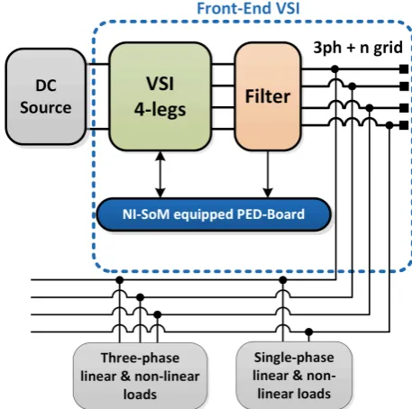
The application addressed by the investigated control strategy relates to a 3-phase 4-wire power supply unit for AC stand- alone loads, which is formed by a 4-leg VSI and its dedicated output power filter as shown in Figure 1. The conceived unit and its control have to be able to support a 3ph+n isolated grid in order to provide power supply to linear and non-linear loads, with either leading or lagging power factor.
II. REPETITIVE CONTROL AND GAIN SCHEDULING Owing to the neutral connection provided by the inverter fourth leg, the whole system can be considered as three fully independent single-phase inverters, and thus can be regulated by individual voltage controllers. This feature effectively decouples the load interaction of the three phases, which is particularly suitable for unbalanced load conditions.
[image:1.595.327.556.303.530.2]The investigated control strategy directly operates in the ABC stationary reference frame. Therefore, from the control design point of view, the plant seen by each voltage controller is an equivalent series characteristic transfer function, consisting of the PWM controlled inverter G inv (z), output filters Gf (z), equivalent load G l (z), and measurement filter G lpf(z), as shown in Figure 2.
Figure 1. Block scheme of a classical generating application.
Figure 2. Block diagram of the output voltage control on each phase.
[image:1.595.321.558.555.614.2]effective use of the resonant + repetitive combined control strategy was demonstrated for the output voltage regulation. The system performance, in term of control quality, overall stability and computational requirements are largely improved when compared to the multi-resonant control solution. With the aim of further enhancing the control performance and improving the overall harmonics regulation performance, the direct repetitive control (dRC) was presented in [5]. Owing to the use of dedicated zero-phase-shift compensators for different load conditions, an even better compensation of high order harmonics has been obtained. In this work, per-phase individual dRCs are considered for the phase-to-neutral voltage regulation of the 4-leg inverter, and a novel gain scheduling algorithm is proposed to improve the system transient performance during load step situations.
A. Direct Repetitive Control
Based on the internal model principle (IMP), repetitive control was initially proposed in [6] for dealing with periodic reference or disturbance signals in control systems. A repetitive controller iteratively adjusts the actuating signal to improve the current cycle performance on the basis of the error signal calculated with respect to the previous cycle. Theoretically, with a suitably designed repetitive controller, the output of a stable feedback system can track the periodic reference signal or/and reject the exogenous periodic disturbance with zero steady state error [7].
Since the 4-leg VSI system, target application of this paper, is internally stable, a direct type repetitive control can be adopted, to simplify the design of the ZPS compensator as discussed in [5].
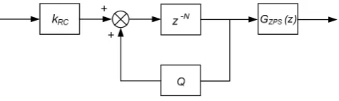
Figure 3 highlights the detailed structure of the dRC controller, where k RC is the repetitive learning gain, N is the ratio between the period of the reference and the digital
- N
[image:2.595.53.291.491.562.2]sampling time, z is the delay line for periodic signal generation, G ZPS (z) is the ZPS stability compensator, and Q is the robustness filter.
Figure 3. Detailed structure of the dRC controller.
The function of the stability compensator G ZPS (z) is to ensure the overall system is stable after including the RC controller. Different filter forms, e.g. low pass filters, can be employed for straightforward implementation. In this work, the ZPS compensator has been chosen to obtain the capability of high order harmonic compensation.
From the dRC control design point of view, the plant is the system open loop transfer function GOL (z), which can be represented in the gain-zero-pole manner as in (1). Since the system is internally stable, all the poles, p1 to pm, are located inside the unity circle. Without loss of generality, by assuming
it contains u un-cancellable zeros and n-u cancellable ones, GOL (z) can be further expressed, where Den(z) represents the
+
denominator; Num (z) and Num-(z) are the cancellable and un- cancellable parts of the numerator, respectively.
+
( - )...( -z1 zn) ( ) -( )
( -z p1)...( -z pm) D ( )z
( ) = um um
OL
en
Based on it, the ZPS compensator can be designed as in (2), - -1
k z z kN z N z
G z = (1)
where Num ) is obtained from Num-(z) with z replaced by 1/z, - (z2
and [N um is calculated by substituting z in Num-(z) with 1.
- −
(1)]
( ) (z 1)
( ) = (2)
( )[ -(1)]2
en um
ZPS
um um
As demonstrated in [5], dedicated ZPS compensators for different load conditions can be designed to achieve unitary gain and zero-phase-shift at the fundamental frequency and at all harmonic points up to Nyquist frequency, which ensures a perfect reference tracking and noise rejecting capability. When the ZPS compensator is applied, the repetitive control system is adequately stable for 0<k RC<2 [5].
The aim of implementing the robustness filter Q is to modify the internal model and thus to increase the system stability margin at the high frequency band [5]. Either moving average filters or close-to-unity constants can be applied. In this work, a close-to-unity constant of 0.99 has been chosen, since it can be easily implemented and modified. This feature is particularly useful for the proposed gain scheduling technique discussed in the following section. Table I lists the parameter of the dRC control system.
TABLE I – PARAMETER OF THE DRC CONTROL SYSTEM.
D z N
G z
kN + z N
fS Sampling frequency 12 kHz
N Delay line 240
Q Robustness filter 0.99
G ZPS(z) Stability filters ZPSs with 1kW span level
k RC Repetitive learning gain 1
B. Gain Scheduling Algorithm
0.5 0.51 0.52 0.53 0.54 0.55 0.56 Time (s)
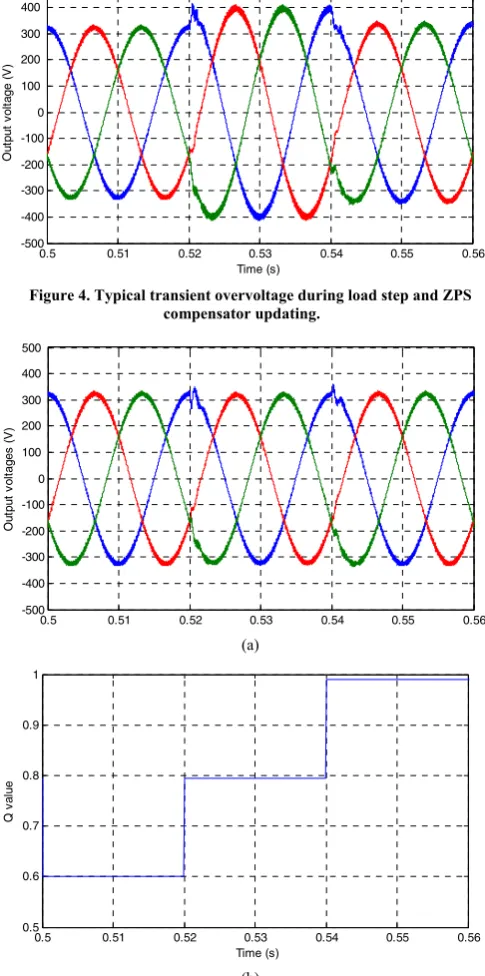
Figure 4. Typical transient overvoltage during load step and ZPS compensator updating.
(a)
[image:3.595.50.293.70.559.2](b)
Figure 5. Transient voltage during load step (a) and ZPS compensator updating, with gain scheduling of Q (b).
With the aim of eliminating the transient overvoltage, a novel gain scheduling algorithm is proposed in this work. For the dRC controller, two parameters can be considered as the candidates for gain scheduling: the repetitive gain kRC and the robustness filter Q. Due to the use of the ZPS compensator, it is preferable to hold k RC at 1, since it ensures a proper stability margin in steady state and fast error converge during transients.
500
400
300
200
100
0
-100
-200
-300
-400
-500
O
u
tp
ut v
ol
ta
ge
(V
)
Q
v
a
lue
O
ut
p
ut v
ol
ta
ge
s
(V
)
0.5 0.51 0.52 0.53 0.54 0.55 0.56 500
400
300
200
100
0
-100
-200
-300
-400
-500
0.5 0.51 0.52 0.53 0.54 0.55 0.56 Time (s)
0.9
0.8
0.7
0.6
0.5 1
Therefore, the robustness filter Q is scheduled during the load step cycles, in order to trim the transient overvoltage out. Figure 5 presents the output voltage waveform under the proposed gain scheduling algorithm, where the testing condition is identical to the one used in Figure 4. The corresponding Q value is also provided.
As it can be seen, when a load step is detected at 0.5s, the robustness filter Q is reduced to a low value of 0.6, and stepped up back to the steady state value of 0.99 through the following 3 cycles. By doing so, the transient overvoltage can be successfully eliminated. This is mainly due to the fact that, the use of a lower value of Q implies a much lower gain at the fundamental frequency and harmonic points, so that the resultant actuating signal is considerably limited accordingly. After the 3 cycles, the value of Q is resumed back to 0.99, which still set a high tracking demand to ensure a high quality output in the steady state.
The selection of the initial value of Q is considered as a trade- off, i.e. a low value can significantly mitigate the transient overshoot, but may cause some under-voltage output. A similar design compromise also applied on the gain scheduling cycle number, i.e. a small cycle number implies that the system can recover back to steady state operation quickly, but some over- voltage output may possibly take place. By evaluating the converter system performance with different set of Q and cycle number, the final values have been chosen at 0.6 and 3, respectively.
Figure 6 illustrates the basic flow chart of the proposed dRC strategy with gain scheduling of Q. For each phase, the load status is continuously monitored by a dedicated hardware chip, i.e. ADE7953 IC. Once a significant load step change is detected, the current actuating signal is recorded for one fundamental period and repeated for the following cycle, which effectively results in an open loop control action.
Figure 6. Flow chart of the proposed direct repetitive control with gain scheduling of Q.
During this open loop cycle, the ZPS parameters are updated according to the evaluated load condition.
[image:3.595.323.567.460.558.2]III. EXPERIMENTAL SETUP AND IMPLEMENTATION
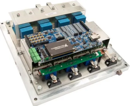
[image:4.595.62.278.154.257.2]The Inverter output filter has been designed according to [8] and its phase-to-neutral representation is shown in Figure 7. Information on damper and trap selection are reported in [8]. The 3-phase 4-leg inverter prototype and its control board are highlighted in Figure 8, whereas its main characteristics are summarized in Table II.
Figure 7. Scheme of the VSI output filter.
TABLE II - 3-PHASE 4-LEG INVERTER PROTOTYPE MAIN CHARACTERISTICS
Rated Power 40 kVA
Line-to-Line Voltage 400±10% V
Switching Frequency 12 kHz
Efficiency @ rated power
(output filter included) 0.97
Power Modules Semikron - SEMIX303GB12Vs DC-Link Capacitors MKP 3 x 150uF – 900Vdc
AC Output Inductors L = 800 μH
AC Output Main Capacitors C = MKP 5 μF – 480Vac
Control Board PED-Board®
[image:4.595.46.298.277.394.2]The proposed dRC algorithm and its Gain Scheduling feature have been implemented in a combined μProcessor-FPGA system. As core technology, the National Instruments System on Module (SoM) has been used [9], formally sbRIO-9651, which is based on the Xilinx ZYNQ-7020 [10]. NI-SoM is supported by an industrial board specifically designed for power electronics and drives applications. The complete dRC structure is then implemented on the FPGA to fully exploit its real parallelism capabilities.
Figure 8. PED-Board on the 3ph 4leg VSI.
Thanks to the National Instruments LabVIEW integrated graphical environment, FPGA and microprocessor (μP) code development is straightforwardly achieved due to its high-level of abstraction features and low-level programming capabilities. With reference to this specific application, FPGA is devoted to provide the interface to the ADCs, PWM channels, DACs and other low-level functionalities.
The whole Repetitive Control structure has been implemented on the FPGA, which is capable to execute it synchronously with the PWM modulator. On the contrary, the gain scheduling algorithm, the output power evaluation and the graphical user interface have been implemented in the on-board dual-core ARM processor. Accordingly, once the RC gains have been evaluated, new coefficients are sent to the FPGA for continuous real-time update.
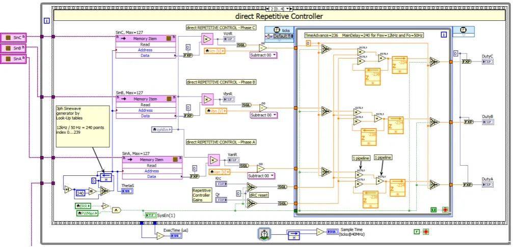
Table III highlights the FPGA requirements concerning the whole algorithm implementation when it is implemented using fixed-point (FXP) or 32-bit single precision floating-point arithmetic (SGL). It can be noticed that the FPGA space requirements are very low, allowing to simply implement multi-converter control or extending the numerical processing to floating-point numeric representation as commonly done in Digital Signal Processor (DSP). LabVIEW block diagram of the FPGA direct Repetitive Control part is shown in Figure 9, where the sinusoidal output voltage reference is generated as a memory defined look-up table and the main dRC is run within a Single Cycle Timed Loop (SCTL) [11].
TABLE III - FPGA RESOURCES WITH FIXED-POINT AND 32-BIT FLOATING- POINT IMPLEMENTATION
FPGA Resources FXP SGL
Slice registers 10.4% 13.5%
Slice LUTs 21.8% 32.9%
Block RAMs 4.3% 4.3%
DSP48s 8.6% 6.4%
IV. EXPERIMENTAL RESULTS
Experimental results are obtained with the whole control algorithm fully operating. Experimental validation started with the verifications of the behavior during steady-state operation. After that, load step tests have been performed to validate the proposed gain scheduling algorithm. The first test shown in Figure 10 is executed in stationary operating conditions, loading the 3-phase 4-leg inverter with a balanced pure resistive load. Each phase has to provide around 2 kW, resulting in a light load state where the output power filter resonance is almost undamped.
[image:4.595.59.287.512.698.2]currents are drawn from the inverter, proving the effectiveness of the illustrated control strategy. Additionally, steady state operating condition were also tested where a 4kW single phase diode bridge AC-DC converter is connected between phase A and neutral, leaving phase B and C at no-load condition. The result is shown in Figure 12, where the load side voltages still exhibits a THD close to zero.
Figure 10. Inverter output voltages and currents for balanced linear load. 200V/div, 20 A/div.
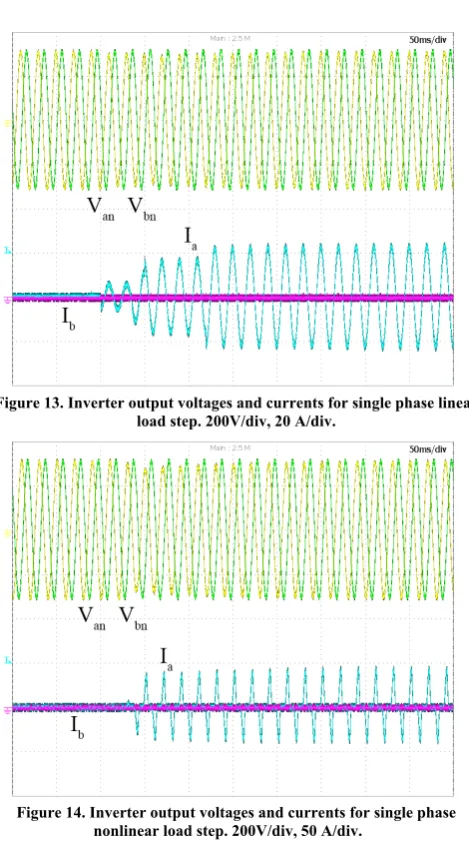
Experimental verification during a load transient is finally executed with both linear and nonlinear loads. At first, a load step is performed with a single phase pure resistive load as shown in Figure 13. As soon as the load is changed, the gain scheduling algorithm evaluates the new control parameters to be updated. As depicted in the figure, the phase A output voltage falls within the limits imposed by the standards, around -5.7%. In case of the nonlinear load step illustrated in Figure 14, obtained from a single phase diode bridge rectifier connected between phase A and neutral, due to the higher
current value and related sharpness, the phase A voltage drops till -10% of its rated value.
[image:5.595.332.553.347.699.2]Figure 11. Inverter output voltages and currents for nonlinear load condition. 200 V/div, 20 A/div.
Figure 12. Inverter output voltages and currents for single-phase nonlinear load condition. 200 V/div, 50 A/div.
[image:5.595.63.280.407.589.2]Figure 13. Inverter output voltages and currents for single phase linear load step. 200V/div, 20 A/div.
Figure 14. Inverter output voltages and currents for single phase nonlinear load step. 200V/div, 50 A/div.
CONCLUSIONS
The direct Repetitive Control strategy with zero-phase-shift capability has been improved by a novel gain scheduling algorithm to be used in stand-alone generating application. Experimental verification highlights better performance of the output voltage regulation during load step variations.
Moreover, as demonstrated by the experimental tests, near-zero THD and fast compensation can be obtained for the inverter output voltages; even when low output capacitance filter is used.
ACKNOWLEDGEMENTS
The Authors are thankful to Mr. Marco Salvi and E.D.Elettronica Dedicata S.r.l. for providing the PED-Board® used in the experimental tests. (ped-board.com).
REFERENCES
[1] H. Yi, F. Zhuo, and F. Wang, “Analysis About Overshoot Peaks Appearing in the Current Loop With Resonant Controller,” IEEE J. Emerg. Sel. Top. Power Electron., vol. 4, no. 1, pp. 26–36, Mar. 2016. [2] D. De and V. Ramanarayanan, “A Proportional-Multiresonant
Controller for Three-Phase Four-Wire High-Frequency Link Inverter,” IEEE Trans. Power Electron., vol. 25, no. 4, pp. 899–906, Apr. 2010. [3] A. Lidozzi, G. Lo Calzo, L. Solero, and F. Crescimbini, “Integral-
resonant control for stand-alone voltage source inverters,” IET Power Electron., vol. 7, no. 2, pp. 271–278, Feb. 2014.
[4] A. Lidozzi, C. Ji, L. Solero, P. Zanchetta, and F. Crescimbini, “Resonant-Repetitive Combined Control for Stand-Alone Power Supply Units,” IEEE Trans. Ind. Appl., vol. 51, no. 6, pp. 4653–4663, Nov. 2015.
[5] A. Lidozzi, L. Solero, F. Crescimbini, C. Ji, and P. Zanchetta, “Load adaptive zero-phase-shift direct repetitive control for stand-alone four- leg VSI,” presented at the 2015 IEEE Energy Conversion Congress and Exposition (ECCE), 2015, pp. 4330–4336.
[6] H. Sato, T. Sueno, T. Toyama, M. Mikawa, T. Toda, and S. Matsumoto, “High accuracy magnet power supply for proton synchrotron by repetitive control,” 1991, pp. 812–816.
[7] M. Tomizuka, T. C. Tsao, and K. K. Chew, “Discrete-Time Domain Analysis and Synthesis of Repetitive Controllers,” in American Control Conference, 1988, 1988, pp. 860–866.
[8] G. Lo Calzo, A. Lidozzi, L. Solero, and F. Crescimbini, “LC Filter Design for On-Grid and Off-Grid Distributed Generating Units,” IEEE Trans. Ind. Appl., vol. 51, no. 2, pp. 1639–1650, Mar. 2015.
[9] “sbRIO-9651 SOM,” National Instruments. [Online]. Available: http://sine.ni.com/nips/cds/view/p/lang/it/nid/212788.
[10] “Zynq-7000 All programmable SoC,” Xilinx. [Online]. Available: http://www.xilinx.com/products/silicon-devices/soc/zynq-7000.html. [11] “An Introduction to High-Throughput DSP in LabVIEW FPGA,”
National Instruments. [Online]. Available: http://www.ni.com/white- paper/13698/en/.