Accepted Manuscript
Selecting suitable image dimensions for scanning probe microscopy James Bowen , David Cheneler
PII: S2468-0230(17)30100-1
DOI: 10.1016/j.surfin.2017.09.003
Reference: SURFIN 135
To appear in: Surfaces and Interfaces
Received date: 27 June 2017 Revised date: 29 August 2017 Accepted date: 10 September 2017
Please cite this article as: James Bowen , David Cheneler , Selecting suitable image dimensions for scanning probe microscopy,Surfaces and Interfaces(2017), doi:10.1016/j.surfin.2017.09.003
ACCEPTED MANUSCRIPT
Selecting suitable image dimensions for scanning probe microscopy
James Bowen
1*, David Cheneler
21
School of Engineering and Innovation, The Open University, Walton Hall, Milton Keynes, MK7 6AA, UK
2
Engineering Department, Lancaster University, Bailrigg, Lancaster, LA1 4YR, UK
* Corresponding author: [email protected]
Abstract
The use of scanning probe microscopy to acquire topographical information from surfaces with nanoscale features is now a common occurrence in scientific and engineering research. Image sizes can be orders of magnitude greater than the height of the features being analysed, and there is often a trade-off between image quality and acquisition time. This work investigates a commonly encountered problem in nanometrology - how to choose a scan size which is representative of the entire sample. The topographies of a variety of samples are investigated, including metals, polymers, and thin films.
Keywords
Atomic force microscopy, roughness, scanning probe microscopy, surface, topography
1. Introduction
Surface metrology can be defined as the measurement of the deviations of a workpiece from its intended shape [1]. This include features such as deviations from roundness, straightness, flatness, cylindricity, and other descriptors of specimen shape. Surface topography measurement also detects the marks left on a specimen in trying to achieve the shape, such as those created by machining or polishing. Surface metrology is also highly relevant to nanotechnology and micro/nanofabrication, for example assessing the structure of thin films manufactured using vapour deposition [2-4], or using focused ion beam to etch surfaces [5-6]. Researchers in these fields represent a range of scientific and engineering disciplines, and hence may be unfamiliar with the complexities of measuring surface topography. It would be helpful if a simple set of rules or guidance could be established regarding topography measurement
The development of the scanning probe microscope, particularly the scanning tunnelling microscope (STM) [7] and the atomic force microscope (AFM) [8], revolutionised the ability to acquire three-dimensional topographical information. These techniques are now well-established as 'go-to' analytical tools when dealing with nanomaterials and nano-engineered surfaces. The versatility of AFM for imaging both conductive and insulating materials means it is particularly popular. Researchers have sought to capture the effect of scanning parameters such as scan speed [9], cantilever dynamics [10], tip size [11], and the choice of medium in which scanning is performed, e.g. liquid environment [12-13]. For example, Westra and Thomson investigated how the finite size of the AFM tip influenced surface profiles [14]. Vertical measures were found to be relatively insensitive to increasing tip size. In contrast, lateral measures became increasingly distorted as tip size increased.
The 1-dimensional average roughness, , of a surface is defined as "arithmetic mean deviation from the centre line through the profile" and is expressed mathematically by Equation 1, in which is the number of pixels in the image, and is the deviation from the centre line for each pixel.
∑ | | (1)
ACCEPTED MANUSCRIPT
ACCEPTED MANUSCRIPT
2. Experimental
2.1 Sample preparation
Samples were immobilised onto steel specimen disks (Agar Scientific, UK) using cyanoacrylate adhesive (Loctite, UK) prior to measurement. If required, samples were trimmed to dimensions of 30 mm x 30 mm or smaller. The samples prepared were
(i) Al2O3 disc (Agar Scientific, UK)
(ii) polished steel disc (Agar Scientific, UK)
(iii) poly(methyl methacrylate) tile (in-house supply) (iv) poly(styrene) Petri dish (BD Falcon, UK)
(v) poly(tetrafluoroethylene) sheet (Altec, UK) (vi) CaF2 window (Crystran, UK)
(vii) Si(100) wafer (IDB Technologies, UK)
(viii) 30 nm Au film thermally evaporated onto Si wafer (Georg Albert PVD, Germany)
(ix) 100 nm CFxOy film deposited onto Si wafer using plasma polymerisation, see Cheneler et al. [15] for further
details.
2.2 Characterisation using AFM
Surface topographies were measured within square scan windows, with equal x- and y-dimensions. The length of the x-dimension is hereafter referred to as the Image Size, . The Image Size was varied in the range 0.1 μm to 100 μm. A line pixel density, , of 512 pixels was employed throughout; this means that images were composed of a square array of pixels measuring 512 x 512.
Images were acquired using a NanoWizard II AFM (JPK Instruments, UK) operating in Contact Mode at a temperature of 18 oC and a relative humidity of <40 %. Rectangular pyramidal-tipped Si cantilevers (CSC17/noAl,
ACCEPTED MANUSCRIPT
3. Results
The results are presented in order of increasing maximum surface roughness. Inset in each figure are the x,y dimensions of the image, as well as the image height scale or z-scale, which is hereafter referred to as . Each figure shows the roughness, Ra, of the surface as a function of Image Size, .
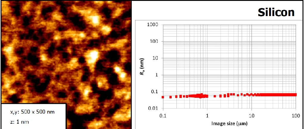
[image:5.595.36.544.174.722.2] [image:5.595.32.542.186.403.2]3.1 Silicon wafer
Figure 1 shows that the surface of a Si wafer exhibits 0.1 nm across the AFM Image Size range 0.1-100 μm. Multiple locations were scanned on the sample, and these data points overlap strongly. The lateral dimensions of the surface features are on the order 50 nm.
ACCEPTED MANUSCRIPT
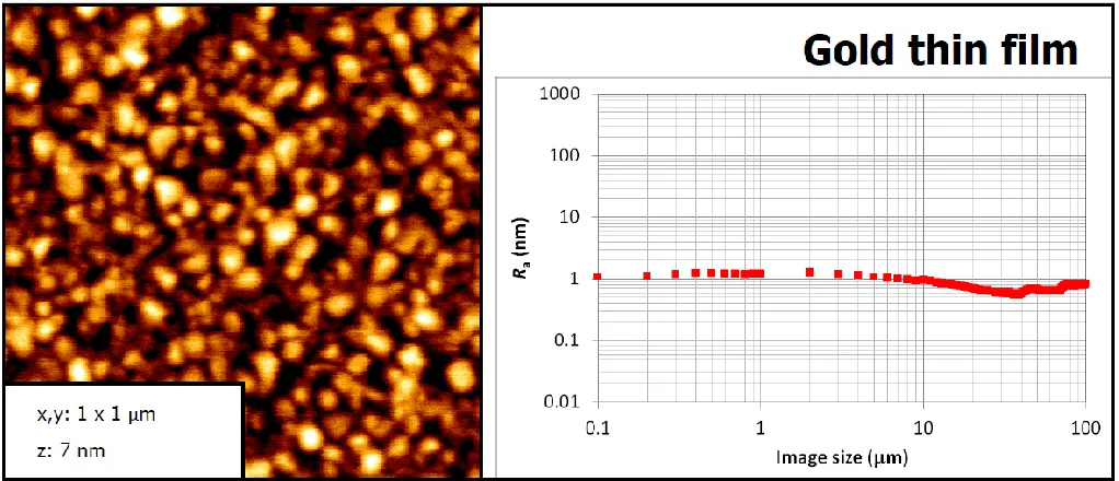
[image:6.595.32.543.155.375.2]3.2 Thermally evaporated Au thin film
Figure 2 shows that the surface of a thermally evaporated Au thin film, deposited onto a silicon wafer, exhibits 1 nm across the AFM Image Size range 0.1-100 μm. The lateral dimensions of the surface features, clusters of Au atoms, are on the order 40-80 nm. In contrast with the Si wafer (Figure 1) however, there exists a maximum , which occurs at 2 μm. For image sizes in the range 2 μm 40 μm there is a gradual decrease in . At 40 μm the increases once again, but does not exceed the maximum measured at 2 μm.
ACCEPTED MANUSCRIPT
[image:7.595.34.544.156.375.2]3.3 Plasma polymerised fluoropolymer thin film
Figure 3 shows that the surface of a plasma polymerised CFxOy thin film, deposited onto a silicon wafer, exhibits
2 nm across the AFM Image Size range 0.1-100 μm. Multiple locations were scanned on the sample, and these data points overlap closely for 5 μm. The lateral dimensions of the surface features, fluoropolymer 'blobs', are on the order 100 nm. Similarly to the Au thin film (Figure 2) the peaks at 2 μm. then decreases slightly for 2 μm 5 μm, before gradually increasing up to 100 μm, albeit with a slight decrease in the range 10 μm 30 μm.
Figure 3. AFM image (x,y = 3 μm; z = 10 nm) and as a function of image size for 100 nm CFxOy film.
[image:7.595.32.544.451.727.2]3.4 Poly(methyl methacrylate) tile
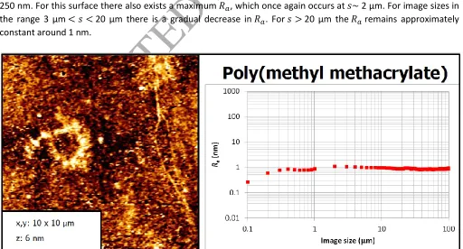
Figure 4 shows that the surface of a poly(methyl methacrylate) tile exhibits 1 nm across the AFM Image Size range 0.4-100 μm. The lateral dimensions of the surface features varies in the approximate range 30 nm 250 nm. For this surface there also exists a maximum , which once again occurs at 2 μm. For image sizes in the range 3 μm 20 μm there is a gradual decrease in . For 20 μm the remains approximately constant around 1 nm.
ACCEPTED MANUSCRIPT
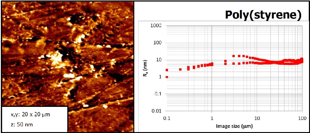
[image:8.595.32.541.156.375.2]3.5 Poly(styrene) Petri dish
Figure 5 shows that the surface of a poly(styrene) Petri dish exhibits roughness in the range 1 nm 20 nm across the AFM Image Size range 0.1-100 μm. Multiple locations were scanned on the sample. The lateral dimensions of the surface features are difficult to characterise using a single parameter, due to the complex topography presented. For this surface there also exists a maximum , around 20 nm, which occurs at 4 μm. For image sizes in the range 4 μm 100 μm the surface roughness remains in the range 6 nm 20 nm.
ACCEPTED MANUSCRIPT
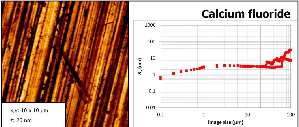
[image:9.595.32.542.170.387.2]3.6 Calcium fluoride window
Figure 6 shows that the surface of a calcium fluoride window exhibits roughness in the range 0.5 nm 3 nm across the AFM Image Size range 0.1 1 μm. The surface roughness remains in the range 2-3 nm for 1 μm 20 μm. Multiple locations were scanned on the sample, which gave rise to a variety of roughness profiles for 20 μm. It is not possible to characterise the lateral dimensions of the complex surface topography using a single parameter. However, there was a dominant direction of polishing marks visible when 30 μm. The lateral dimensions of these surface features lies in the approximate range 75 nm 150 nm. In all instances, increased significantly for 20 μm, approaching a maximum of 40 nm at 100 μm.
ACCEPTED MANUSCRIPT
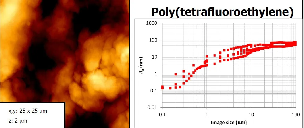
[image:10.595.35.542.144.358.2]3.7 Poly(tetrafluoroethylene) sheet
Figure 7 shows that the surface of a poly(tetrafluoroethylene) sheet exhibits increasing roughness in the range 0.15 nm 90 nm across the AFM Image Size range 0.1-100 μm. Multiple locations were scanned on the sample, which gave rise to a variety of roughness profiles. The surface topography was not suitable for characterisation using a single parameter for the lateral structure. For 40 μm, the surface roughness presented was usually in the range 40 nm 90 nm.
ACCEPTED MANUSCRIPT
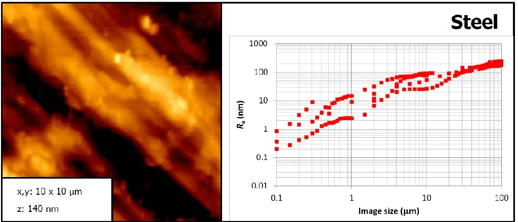
[image:11.595.32.544.125.345.2]3.8 Steel disc
Figure 8 shows that the surface of a steel disc exhibits increasing roughness in the range 0.2 nm 250 nm across the AFM Image Size range 0.1-100 μm. Multiple locations were scanned on the sample, which gave rise to a variety of roughness profiles. For 30 μm, the surface roughness presented was greater than 100 nm, increasing to 250 nm at 100 μm.
ACCEPTED MANUSCRIPT
3.9 Aluminium oxide disc
[image:12.595.40.541.142.359.2] [image:12.595.61.347.380.656.2]Figure 9 shows that the surface of an aluminium oxide disc exhibits increasing roughness in the range 0.4 nm 400 nm across the AFM Image Size range 0.1-100 μm. Multiple locations were scanned on the sample, which gave rise to a variety of roughness profiles. For 2 μm, the surface roughness presented was less than 8 nm, increasing to 160 nm at 10 μm for one sample. Other samples did not exhibit such a strong dependence on the location on which imaging centred.
ACCEPTED MANUSCRIPT
4. Discussion
4.1 Effect of pixel density
The samples can be divided into two categories: (a) those with surfaces which can be defined by a single lateral dimension; and (b) those with surfaces which are too complex to define using a single parameter. For the range of Image Sizes used in this work, 0.1 µm 100 µm, only the poly(methyl methacrylate) tile, Si(100) wafer, 30 nm Au film, and 100 nm CFxOy film fall into category (a). The CaF2 window, Al2O3 disc, poly(styrene) Petri dish, and
poly(tetrafluoroethylene) sheet, and steel disc all fall into category (b).
For samples in category (a) there appears to be a critical image size at which the measured surface roughness reaches an apparent maximum. Such behaviour is an artefact of there being insufficient pixel density available with which to construct the smallest surface features. As the image size increases further, the measured surface roughness decreases slightly, contrary to expectations. If each image size successfully captured the 'character' of the surface, there should be no decrease in roughness, unless a region of different topography were encountered as the scan area increased.
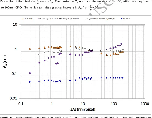
Using the data for the poly(methyl methacrylate) tile, Si(100) wafer, 30 nm Au film, and 100 nm CFxOy film, Figure
10 is a plot of the pixel size, , versus . The maximum occurs in the range , with the exception of
the 100 nm CFxOy film, which exhibits a gradual increase in from
Figure 10. Relationship between the pixel size, , and the average roughness, , for the poly(methyl methacrylate) tile, Si(100) wafer, 30 nm Au film, and 100 nm CFxOy film.
[image:13.595.34.542.293.687.2]ACCEPTED MANUSCRIPT
work, values of 20 yielded values of which did not appear to be compromised by inappropriate choice of scanning parameters relative to the dimensions of surface features.
With regards to the samples in category (b), these surfaces exhibited hierarchies of features, resulting in surface roughness profiles which tended to yield increasing values of with increasing values of . Further, scanning multiple regions of the same sample gave little overlap between roughness curves, particularly for 1 μm. Practical advice which could be applied when measuring samples such as these must include (i) scan multiple locations, (ii) scan multiple image sizes, (iii) consider acquiring data using a measurement technique which operates at lateral length scales greater than AFM, such as profilometry.
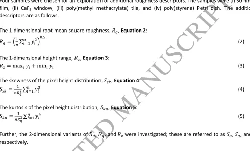
4.2 Choice of roughness descriptors
Four samples were chosen for an exploration of additional roughness descriptors. The samples were (i) 30 nm Au film, (ii) CaF2 window, (iii) poly(methyl methacrylate) tile, and (iv) poly(styrene) Petri dish. The additional
descriptors are as follows.
The 1-dimensional root-mean-square roughness, , Equation 2:
( ∑ ) (2)
The 1-dimensional height range, , Equation 3:
(3)
The skewness of the pixel height distribution, , Equation 4:
∑ (4)
The kurtosis of the pixel height distribution, , Equation 5:
∑ (5)
Further, the 2-dimensional variants of , , and were investigated; these are referred to as , , and respectively.
The pixel height distributions for the four samples are shown in Figure 11. For clarity of presentation, histograms from regularly spaced image sizes are shown. The distribution of pixel heights is approximately symmetric for Au, poly(methyl methacrylate), and poly(styrene), whereas for CaF2 the distribution displays asymmetry at all image
sizes.
Figures 12-15 show the descriptor comparisons for Au, CaF2, poly(methyl methacrylate), and poly(styrene)
respectively. For each sample, each pair of 1-dimensional and 2-dimensional descriptors follows the same trend as a function of image size. There is little difference in value between each descriptor pair for Au, CaF2, and
[image:14.595.33.523.212.509.2]ACCEPTED MANUSCRIPT
Figure 11. Pixel height distributions as a function of image size for (a) Au, (b) CaF2, (c) poly(methyl methacrylate),
(d) poly(styrene).
Figure 12. Roughness descriptors as a function of image size for Au: (a) vs , (b) vs , (c) vs , (d)
[image:15.595.32.515.380.702.2]ACCEPTED MANUSCRIPT
Figure 13. Roughness descriptors as a function of image size for CaF2: (a) vs , (b) vs , (c) vs , (d) vs .
Figure 14. Roughness descriptors as a function of image size for poly(methyl methacrylate): (a) vs , (b) vs , (c) vs , (d) vs .
(a)
(b)
[image:16.595.33.514.376.702.2]ACCEPTED MANUSCRIPT
ACCEPTED MANUSCRIPT
5. Conclusion
This work sought to investigate the influence of the choice of analysis conditions when measuring surface topography using atomic force microscopy. In particular, the importance of pixel density and image dimensions. The topography of nine samples were measured using square images of x,y-dimensions in the range 0.1-100 μm. The average roughness of each image was calculated and plotted as a function of image size. Where possible, the approximate dimension of the smallest surface feature was also defined.
Pixel sizes smaller than 20 nm appeared to be optimal for the characterisation of surfaces with nanoscale topography. Increasing the pixel density of an image should afford the possibility of imaging larger areas without compromising feature resolution. Surfaces which exhibit a hierarchy of topographies should be treated cautiously, and may not be suitable for nanoscale analysis unless well-defined regions free from machining marks are highlighted and analysed in isolation.
ACCEPTED MANUSCRIPT
Acknowledgments
The JPK Instrument NanoWizard II AFM used in this research was obtained through Birmingham Science City: Innovative Uses for Advanced Materials in the Modern World (West Midlands Centre for Advanced Materials Project 2), with support from Advantage West Midlands (AWM) and part funded by the European Regional Development Fund (ERDF).
References
1. Whitehouse, D.J.; Handbook of Surface and Nanometrology, 2nd Edition, CRC Press (Boca Raton), 2011. 2. Reichelt, K.; Lutz, H.O.; Hetero-epitaxial growth of vacuum evaporated silver and gold, J. Cryst. Growth, 1971,
103-107.
3. Chidsey, C.E.D.; Loiacono, D.N.; Sleator, T.; Nakahara, S.; STM study of the surface morphology of gold on mica, Surf. Sci., 1988, 45-66.
4. DeRose, J.A.; Thundat, T.; Nagahara, L.A.; Lindsay, S.M.; Gold grown epitaxially on mica: conditions for large area flat faces, Surf. Sci., 1991, 256, 102-108.
5. Sabouri, A.; Anthony, C.J.; Bowen, J.; Vishnyakov, V.; Prewett, P.D.; The effects of dwell time on focused ion beam machining of silicon, Microelectronic Eng., 2014, 121, 24-26.
6. Sabouri, A.; Anthony, C.J.; Prewett, P.D.; Bowen, J.; Butt, H.; Effects of current on early stages of focused ion beam nanomachining, Mater. Res. Exp., 2015, 2, 055005.
7. Binnig, G.; Rohrer, H.; Gerber, C.; Weibel, E.; Surface studies by scanning tunneling microscopy, Phys. Rev. Lett., 1982, 49, 57-61.
8. Binnig, G.; Quate, C.F.; Gerber, C.; Atomic force microscope, Phys. Rev. Lett., 1986, 56, 930-933..
9. Butt, H-J.; Siedle, P.; Seifert, K.; Fendler, K.; Seeger, T.; Bamberg, E.; Weisenhorn, A.L.; Goldie, K. Engel, A.; Scan speed limit in atomic force microscopy, J. Microscopy, 1993, 169, 75-84.
10. Kühle, A.; Sørensen, A.H.; Zandbergen, J.B.; Bohr, J.; Contrast artifacts in tapping tip atomic force microscopy,
Appl. Phys. A, 1998, 66, S329-S332.
11. Sedin, D.L.; Rowlen, K.L.; Influence of tip size on AFM roughness measurements, Appl. Surf. Sci., 2001, 182, 40-48.
12. de Souza, E.F.; Douglas, R.A.; Teschke, O.; Atomic force microscopic imaging in liquids: effects of the film compressed between the substrate and the tip, Langmuir, 1997, 13, 6012-6017.
13. Ohnesorge, F.; Towards atomic resolution non-contact dynamic force microscopy in a liquid, Surf. Interface Anal., 1999, 27, 379-385.
14. Westra, K.L.; Thomson, D.J.; Effect of tip shape on surface roughness measurements from atomic force microscopy images of thin films, J. Vac. Sci. Technol. B, 1995, 13, 344-349.