Abstract— A flexible architecture is proposed in this paper for implementation Discrete Wavelet Transform (DWT) of 5/3 filter. The proposed architecture includes transforms modules, a RAM and bus interfaces. This architecture works in non separable fashion using a serial-parallel filter with distributed control to compute all the DWT (1D-DWT and 2D-DWT) resolution levels. The so-called lifting scheme represents the fastest implementation of the DWT. A VHDL model was described and synthesized using implementation of our architecture. Synthesis results show that Xilinx XCV600E FPGA implementation can be achieved with a frequency of about 108 Mhz, allowing processing rate between 85 and 187 frames per second for a range of standard picture dimensions. Speed/Area resulting from this processor is analyzed and is shown to demonstrate that our design achieves favourable performances with other FPGA based implementations.
Index Terms— Architecture, DWT, Flexible, Lifting Scheme, 5/3 filter.
I. INTRODUCTION
For multimedia processing, Discrete Wavelet Transform (DWT) based image coding has better performance than traditional DCT based image coding, especially for low bit-rate applications [1]. Therefore many famous coders have been proposed to effectively compress images or frames processed via DWT. Besides, the DWT is employed in JPEG2000, the new standard for image compression, where the 9/7 and the 5/3 wavelet filters are employed as the default filters for lossy and lossless compression respectively. DWT has traditionally been implemented by convolution or the finite impulse response (FIR) filter bank structures. Such implementations require both large number of arithmetic computations and a large storage, features that are not desirable for either high speed or low power image/video processing applications.
Therefore a new approach is called the lifting scheme based wavelet transform or simply lifting has been proposed by Swelden based on a spatial construction of the wavelet and a very versatile scheme for its factorisation has been suggested in [2]. The architecture lifting-based 2D-DWT developed in [3] has regular data flow and low control complexity, and achieves 100% hardware utilization. The other architecture
Manuscript received March 24, 2009; revised 18 April 2009. This work was supported by Electronic and Microelectronic Laboratory, Monastir.
Dhaha Dia is with Electronic and Microelectronic Laboratory, Faculty Sciences of Monastir, 5000 Tunisia (phone: 00216-22-187-144; fax: 00216-73-501785; e-mail: [email protected]).
was based propriety of perfect reconstruction of filter bank developed in [4]. Many architectures of DWT were proposed in literature combined lossy and lossless transform like [5], the aim of this brief is to embed the 5/3 wavelet computation into the 9/7, in order to exploit as much as possible the 5/3 results to achieve the 9/7 ones, with a reduced number of adders compared to other solutions. In [6] the proposed architecture can be reconfigured for 5/3 and 9/7 wavelet transforms. This reduces significantly the required numbers of the multipliers, adders and registers, as well as the amount of accessing external memory, and leads to decrease efficiently the hardware cost and power consumption of design. In [7] the architecture for 1D-DWT principle can be extended to architectures for separable 2D-DWT like the one developed in [8], [9]. The other based pyramid algorithm was developed in [10].
In this paper our architecture is serial-parallel based bi-orthogonal filter it implement 1D-DWT and 2D-DWT, therefore we get a design of DWT reconfigurable with the multi-levels resolution for the up needs. We describe our architecture of DWT decomposition using lifting scheme structure with distributed control to compute all the resolution levels of DWT. This architecture is reconfigurable and scalable in its totality, since we change the levels and types of transforms (1D-DWT or 2D-DWT) without changing the design of the control units.
The remaining paper is organized in the following manner: the next section provides a brief overview of the lifting scheme DWT algorithm. In the section 3, the proposed architecture system and its internal components are described in details. The synthetic results of the FPGA implementation are given in the section 4. Comparisons results with other architectures related works are also presented in section 5. Finality, conclusions are discussed in section 6.
II. DWTBYLIFTINGSCHEME
The lifting scheme is an algorithm used for implementation hardware and software of DWT; it is constituted of steps of
Image
Low Pass High Pass
Split Prediction Up dating +
+
k
1 −
k
Fig.1 Lifting scheme forward transform
Multi-level Discrete Wavelet Transform
Architecture Design
predictions and updating described by the Fig.1.
The advantage of lifting scheme is the forward and inverse transform was obtained from the same architecture. The inverse goes from right to the left, by inversing the coefficients of normalized and changes the sign positive to negative.
Where
k
is the constant of normalisation and the steps of the predictions and the updating at decomposition in polyphase matrix. The polyphase representation of discrete filterh
(
n
)
is defined as:)
(
)
(
)
(
z
h
z
2z
1h
z
2h
=
e+
− o (1)where
h
e(
z
)
andh
o(
z
)
are respectively obtained from the even and odd zeta transform respectively. If we represent)
(
z
h
andg
(
z
)
the low pass and high pass coefficients of the synthesis filter respectively, the polyphase matrix written as:=
)
(
)
(
)
(
)
(
)
(
z
g
z
h
z
g
z
h
z
p
o o e e (2)The filters
h
e(
z
)
,h
o(
z
)
,g
e(
z
)
andg
o(
z
)
are Laurent polynomials, as the set of all polynomials exhibits a commutative ring structure, within which polynomial division with remainder is possible, long division between two Laurent polynomials is not a unique operation. In Euclidean algorithm decomposition can be used, the polyphasep
(
z
)
is finally obtained as:=
∏
= k k z t z s z p i m i i 1 0 0 1 ) ( 0 1 1 0 ) ( 1 ) ( 1 (3)Where
s
i(
z
)
andt
i(
z
)
primary lifting and dual lifting steps filters respectively,k
is a constant of normalisation at low and high coefficients filters.The 5/3 wavelet filter transform is more suitable lossless data compression adopted in JPEG2000 and 9/7 filter is used in JPEG2000 for lossy compression data. The 5/3 filter has one prediction and one up-dating compared to two predictions and two up-dating for 9/7 filter. The following steps are necessary to get their wavelet coefficients as the following tapes for 5/3 filter: Split the input signal (image) into coefficients at odd and even positions. Perform a predict step, that is the operation given below in (4). Perform up-dating step which is the operation given below in (5).
+ + − + = + 2 ) 2 2 ( ) 2 ( ) 1 2 ( ) 1 2
( n x n x n x n
d (4)
+ + + − + = 4 2 ) 1 2 ( ) 1 2 ( ) 2 ( ) 2
( n x n d n d n
a (5)
These equations are illustrate and presented in the Fig.2 for
direct lifting scheme of bi-orthogonal 5/3 filter, where the constant
k
is equal unit.X
)
1
2
(
n
+
d
)
2
(
n
a
2 [ (2) (2 2)]2
1 + +
− X n X n [ (2 1) (2 1) 2] 4
1d n− +d n+ +
+
+
)
1
2
(
n
+
X
)
2
(
n
X
L HFig.2 Lifting scheme decomposition of 5/3 filter The lifting based implementation of two levels 2D-DWT may be computed using filter banks as shown in Fig.3. The input samples X(n) are passed through two stages of analysis filters. They are first processed by low-pass (h(n)) and high-pass (g(n)) horizontal filters and are sub sampled by two. Subsequently, the outputs (L1, H1) are processed by
low-pass and high-pass vertical filter. Note that: L1, H1 are
the outputs of 1D-DWT; LL1, LH1, HL1 and HH1 one-level
decomposition of 2D-DWT.
X(n)
Vertical filter H1
L1
h(n) 2
2 h(n) g(n) h(n) g(n) 2 2 2 2 g(n) LL1 LH1 HL1 HH1 Horizontal filter H2 L2
h(n) 2
2 h(n)
g(n) g(n) 2
2 2 g(n) LL2 LH2 HL2 HH2
h(n) 2
Vertical filter Horizontal filter
Fig.3 Subband decomposition for two-level 2D-DWT
III. OURPROCESSORDESIGNAND IMPLEMENTATION
This section presents the architecture design of our programmable DWT processor. This processor can perform the 1D-DWT and 2D-DWT with multi-levels decomposition upon in the user needs.
A. Components of our processor design
A block based top-level implementation of our proposed processor is shown in Fig.4. The proposed system supports seven blocks. The architecture shown one level decomposition but it is reconfigurable for the multi-levels decomposition in our need.
In this Fig.4, basic units of the architecture system are shown. The following units are:
A Bus Interface Unit has been integrated in order to achieve communication efficiently with the external environment.
initialization phase, the user with the appropriate write commands selects the decomposition DWT type (1D-DWT, 2D-DWT and with multi-levels decompositions). The Control Unit coordinates all system operations and processes. After the initialization phase, the control unit is totally responsible for the system operation. The control unit manages the operation of 2D-DWT serial-parallel even-odd filter (Fig.2). It controls the data input, the synchronization of the operations, and the data output.
The block processing elements: each of them contains a multiplier and an adder. Every five clock cycle one processing element is generated for band H and band L transformed pixels. The block has the higher computation task of our architecture.
The blocks processing band H and band L are needed in the case of 2D-DWT and multi levels decompositions. These blocks used the arithmetic logic operation of details and approximation coefficients respectively. The RAM block is used for storage of the L and H coefficients for the next transformations types (2D-DWT or multi levels decomposition).
The output accumulator is the final block in the architecture. This produces output data by storing the results of different transformations; it is generated under the control of a synchronous available signal.
Band LH
Bloc 1D-DWT
Band HH
Band LL
1D-DWT
2D-DWT Band
H Band L
Band LL Band LH
Band HL Band HH One Level
Transformed Pixels
Control Start Bus Interface
Unit Processing
Controller Unit
Processing Band H
Processing Band L
Output Accumulator
B
an
d
L
Vector Pixels Pixels
Mode Level Load
RAM
B
an
d
H
Band HL
Fig.4 Our direct DWT Architecture Design
B. Working Procedures
Our design presents various transformations like the 1D-DWT, 2D-DWT and multi level decomposition of DWT. The decomposition scheme is level by level and described as follows:
The 2D-DWT, in first-level decomposition, the bus interface unit selects data (pixels) form input image. The transform module (Processing, processing band H and processing band L) decomposes to the four sub-bands LL1,
LH1, HL1 and HH1, and saves LL1 band to the RAM module.
After finishing the first level decomposition, the controller unit selects data from RAM module. The LL1 band is then
sent to the module transform to perform the second level decomposition. The transform module decomposes the LL1
band to the four sub-bands LL2, LH2, HL2 and HH2, and
saves LL2 band to the RAM module for next level
decomposition. This procedure repeats until the desired N level (last level) decomposition is finished. The 1D-DWT, in
first-level decomposition the bus interface unit selects data (pixels) form input image. The transform module (Processing) decomposes to the two sub-bands L1 and H1 and
saves L1 band to the RAM module. In second level the
controller unit selects data (band L1) from RAM module. The
module transform (processing band L) decompose the band L1 to the two sub-bands L2 and H2 and save band L2 to the
RAM module for next level decomposition. They blocs of process are shown in Fig.5.
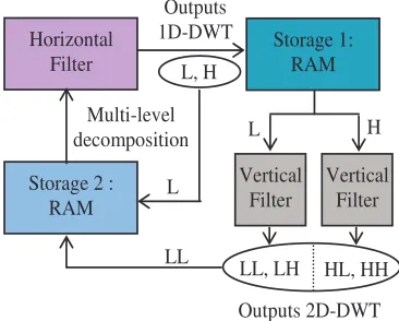
L Outputs 1D-DWT
L, H
Outputs 2D-DWT Multi-level
decomposition
LL
H L
Horizontal Filter
Vertical Filter
Storage 1: RAM
Storage 2 : RAM
LL, LH
Vertical Filter
[image:3.595.339.522.182.329.2]HL, HH
Fig.5 Serial-Parallel module transforms
IV. EXPERIMENTS RESULTS
The implementation of multi-level decomposition of 1D-DWT or 2D-DWT for image clock of size 256
×
256 is carried out Lifing Scheme (L.S) using Xilinx XCV600E. In our implementation, the number of logic elements, number of registers and the maximum operating frequency are computed and the synthetic results are given in Table I.We implemented an xilinx FPGA design that efficiently performs both 1D-DWT and 2D-DWT depending up on the control signals start and mode. Fig.4 shows the top level schematic of the integrated chip. When mode = ‘01’, it signals the data path unit that 1D-DWT with band L transformed needs to be performed. Similarly, if mode = ‘11’, 2D-DWT and band L transformed will be performed. When mode = ‘00’ or ‘10’ 1D-DWT or 2D-DWT directly must be configured. The described design has been implemented in VHDL using the ModelSim Simulator and synthesized, placed, and routed using target device of Xilinx XCV600E FPGA. The [image:3.595.55.293.363.540.2]architecture was simulated for verification of the correct functionality, by using the test images.
Table I FPGA Synthesis results
Parameter Values
Number of Slices 1835
Number of DFFs 1656
Number of LUTs 3359
Number of IOs 48
Number of GCLKs 1
Frequency (Mhz) 108
Power (mW) 47
number of GCLKs, large number of LUTs and middle number of Slices. Therefore our architecture requires less FPGA resources (LUTs, Slices) than others architectures like the one
developed in [12]. In simulations, we used 256×256 Lena coded with 8 bpp, this was taken as input for evaluating the 1D-DWT or 2-D DWT with multi-levels decompositions algorithm. Our architecture transfers image into two or more filtered and decimated image corresponding to different frequency sub-bands. The number of decompositions performed on original image obtaining sub-bands is called sub-band decomposition level.
Table II, shows computation time our architecture with different three levels decomposition of 1D-DWT and 2D-DWT for Lena and Barbara images. We find that the computation time increase according to the increase level decomposition for both DWT (1D and 2D) in them two images. The computation time of 1D-DWT are less than 2D-DWT in all decomposition levels, because the 1D-DWT uses only the bloc of processing. In opposition to 2D-DWT in this process, our architecture use three processing blocs: the bloc processing, the processing band L and processing band H. therefore our 2D-DWT process present highest time than 1D-DWT. The multi-level decomposition takes n level computation of DWT for 1D-DWT or 2D-DWT. The n level decomposition takes n times for the corresponding transform of DWT. In all case our architecture has the fastest computing time small 3ms compared than as architecture in [7], for three level decompositions. The computation time has been normalized to the same internal clock rate and calculated by the following equation (6):
(
)
21 2
3 2
2 2 2 2
1 1
2
4
1
3
2
4
...
4
4
4
2
1
4
2
1
N
T
N
N
N
N
N
T
N
T
L
L L
i i
−
− = −
−
=
+
+
+
+
+
=
=
(6)
[image:4.595.357.506.242.373.2]Where the parameter;
N
2is the image size, and L the level decomposition DWT (1D-DWT or 2D-DWT).Table II Computation time of three levels
1D-DWT 2D-DWT
Time (ms) Time(ms)
Level
decomposition decomposition Level Images
Size (256×256)
1st 2nd 3rd 1st 2nd 3rd
Lena 1.23 1.54 2.05 2.36 2.42 2.62 Barbara 1.54 1.76 1.89 2.45 2.65 2.93
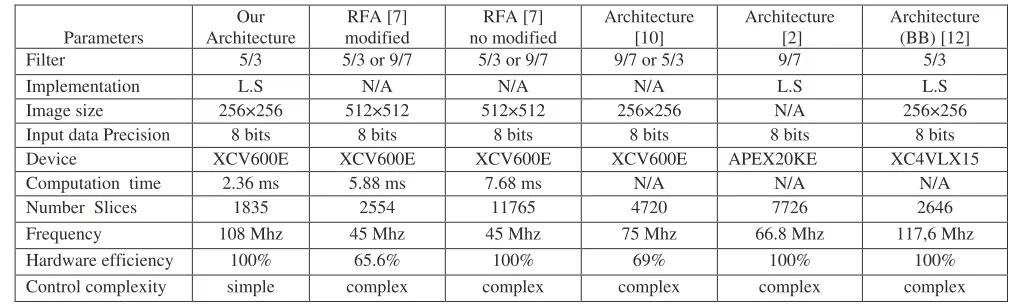
V. PERFORMANCES AND COMPARISONS
In this section, we present the different performance of our architecture serial-parallel and compare the results with the Recursive Pyramid Algorithm (RFA), modified in [7] and,
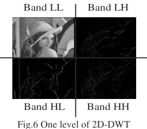
with Pyramid Algorithm Analysis developed in [10], which have the same device of our architecture. We compare our architecture with other different device like the recent work of implementation of 5/3 lifting architectures Based-Block (BB) implementation in FPGAs developed in [12], and architecture developed in [2] similar in our architecture. Therefore, this performance comparison of different architectures is presented in Table III. Our architecture uses serial input of read data (pixels of image) and parallel processing of different pixels. Therefore we compare our architecture with different topologies of 2D-DWT architectures. Our architecture is efficient and flexible like the one parallel architecture developed in [12]. In Fig.6 we showed one decomposition level Lena image of 2D-DWT by lifting scheme 5/3 filter of our architecture. We show in this Fig.6 the different bands of 2D-DWT.
Band HH Band HL
Band LH Band LL
Fig.6 One level of 2D-DWT
Table III, compares the hardware performance of the implemented architecture. This table presents comparative results of our architecture, in terms of frequency, number of FPGA slices, computing time, hardware efficiency and control complexity with others architectures. We compare our architecture at 108 Mhz with three other using same
XCV600E device; the modified RPA [7] at 45 Mhz, the no
modified RFA [7] at 45 Mhz and architecture in [10] at 75 Mhz.
We compare it again with other different devices; architecture APEX20KE [2] at 66.8 Mhz and architecture BB
XC4VLX15 in [12] at 117.6 Mhz. As well as being highly
scalable, our architecture requires 108 Mhz frequency for clock cycles. It uses the minimum storage unit RAM size possible to perform the transform. In other comparisons to the same device architectures given in [7] (modified RPA and no modified RPA) and architecture in [10]. Our architecture requires 2,36 ms computation time compared to 5,88 ms and 7,68 ms respectively for the modified RPA [7], and the no modified [7]. In number slices ours requires only 1835 slices compared to the 2554 slices for the modified RPA, 11765 slices for the no modified RPA and 4720 slices for architecture in [10]. In hardware efficiency our architecture is 100% used, compared to the modified RPA in [7] where 65.6% is used and 69% for the architecture in [10]. Therefore our architecture presents more advantages compared than the other architecture using same device.
[image:4.595.55.280.434.544.2] [image:4.595.57.282.589.719.2]compared to the other two architectures. In all different
[image:5.595.42.557.107.259.2]comparisons, our architecture presents a complexity simpler than that of all the other presented architectures.
Table III Performance and Comparisons 2D-DWT of our Architecture
Parameters Architecture Our modified RFA [7] no modified RFA [7] Architecture [10] Architecture [2] Architecture (BB) [12]
Filter 5/3 5/3 or 9/7 5/3 or 9/7 9/7 or 5/3 9/7 5/3
Implementation L.S N/A N/A N/A L.S L.S
Image size 256×256 512×512 512×512 256×256 N/A 256×256
Input data Precision 8 bits 8 bits 8 bits 8 bits 8 bits 8 bits
Device XCV600E XCV600E XCV600E XCV600E APEX20KE XC4VLX15
Computation time 2.36 ms 5.88 ms 7.68 ms N/A N/A N/A
Number Slices 1835 2554 11765 4720 7726 2646
Frequency 108 Mhz 45 Mhz 45 Mhz 75 Mhz 66.8 Mhz 117,6 Mhz
Hardware efficiency 100% 65.6% 100% 69% 100% 100%
Control complexity simple complex complex complex complex complex
VI. CONCLUSION
In this work we have proposed flexible architecture for the implementation of multi-level decomposition DWT (1D and 2D) by 5/3 filter. A VHDL based methodology has been used targeting FPGA design. The results of the synthesis on a xilinx XCV600E show a working frequency of 108 MHz
allowing the processing of images sized 256×256 pixels. Our architecture has the lowest hardware cost in comparison to the different parameters include in table III. Therefore, our architecture has been correctly verified as 100% hardware utilisation, fast computing time and low control complexity. Our works are suitable for the next generation image/video compression using multilevel decomposition DWT.
REFERENCES
[1] M.A. Suhail and M.S. Obeidat “One digital Watermarking in JPEG
2000” Electronics, Circuits and Systems. The 8th IEEE International
Conference on Volume 2, ICECS 2001, Pages: 871- 874.
[2] T. Acharya and C. Chakrabarti “A Survey Lifting-based Discrete
Wavelet Transform Architectures” Journal of VLSI Signal Processing 42, 321-339,13 February 2006.
[3] S. Barua, J.E. Charletta, K.A. Kotteri and A.E. Bell “An efficient
architecture for lifting-based two-dimensional discrete wavelet transforms” Intergration, the VLSI Journal 38, 341-352, 21 July 2004.
[4] K. A. Kotteri, A. E. Bell and J. E. Carletta “Design of Multiplierless,
High-Performance, Wavelet Filter Banks With Image Compression Applications” IEEE Transactions Circuits and Systems – I: Regular Papers, vol. 51, N° 3, March 2004.
[5] M. Martina and G. Masera “Multiplierless, Folded 9/7-5/3 Wavelet
VLSI Architecture” IEEE Transactions on Circuits and Systems- II:Express Briefs, vol.54 N°. 9, September 2007.
[6] X. Chengyi, T. Jinwen and L. Jian “ Low complexity reconfigurable
architecture for the 5/3 and 9/7 discrete wavelet transform” Journal of Systems Engineering and Electronics vol. 17 N° 2, pp. 303-308, 2006.
[7] R.J.C. Palero, R.G. Gironés and A.S. Cortes “A Novel FPGA
Architecture of a 2-D Wavelet Transform” Journal of VLSI Signal Processing 42, 273-284, August 4, 2005.
[8] P.C. Wu and L.G. Chen “An efficient architecture for two-dimensional
discrete wavelet transform” IEEE Transaction on Circuit and Systems and Systems for Video Technology, Volume 11, N° 4, April 2001, Pages 536-545.
[9] J. Jyotheswar and S. Mahapatra “Efficient FPGA implementation of
DWT and modified SPIHT for lossless image compression” Journal of Systems Architecture 53, 369-378, 19 January 2007.
[10] A. Benkrid, D. Crookes and K. Benkrid “ Design and Implementation
of Generic 2-D Biorthogonal Discrete Wavelet Transform on an
FPGA” IEEE, Proceedings of the 9th Annual IEEE Symposium on
Field-Programmable Custom Computing Machines, 2001.
[11] A. Pande, J. Zambreno “Design and analysis of efficient reconfigurable
wavelet filter” IEEE of Internnational Conference on Volume, issue 18-20, May 2008, Pages: 327-332.
[12] M.E. Angelopoulou, P.Y.K. Cheung, K. Masselos and Y.