Versatile High-level Synthesis of Self-checking Datapaths
Using an On-line Testability Metric
Petros OIKONOMAKOS
Mark ZWOLINSKI
Bashir M. AL-HASHIMI
Electronic Systems Design Group
Department of Electronics and Computer Science
University of Southampton
Southampton SO17 1BJ
United Kingdom
{po00r,mz,bmah}@ecs.soton.ac.uk
Abstract
There have been several recent attempts to include duplication-based on-line testability in behaviourally synthesized designs. In this paper, on-line testability is considered within the optimisation process of iterative, cost function-driven high-level synthesis, such that on-line testing resources are inserted automatically without any modification of the source HDL code. This involves the introduction of a metric for on-line testability. A variation of duplication testing (namely inversion testing) is also used, providing the system with an additional degree of
freedom towards minimising hardware overheads
associated with test resource insertion. Considering on-line testability within the synthesis process facilitates fast
and efficient design space exploration, resulting in a versatile high-level synthesis process, capable of producing alternative realisations according to the designer’s directions.
1. Introduction and Motivation
In designs with high reliability requirements, or when faults are expected to develop due to a hostile environment, some form of on-line testing (ideally combined with a recovery mechanism) is essential to guarantee the correct operation of the system. Typically, computed results are verified using a self-checking design technique. Several such techniques have been presented [1]; simulation results ([2]) show that parity checking and (identical or diverse) duplication are the most attractive, both in terms of fault coverage and of area overhead. In this work, we apply duplication-related techniques, taking advantage of the hardware saving potentials naturally existing in data paths, as is demonstrated in the following example.
Straightforward physical duplication clearly results in a hardware penalty of over 100%. However, when dataflow graphs (DFGs) are considered (rather than isolated cir-cuits), then algorithmic duplication, utilising components’
idle periods* can provide an economical alternative.
Consider figure 1, where three operations of the same type (additions) are scheduled over control steps (CS) 1 and 2,
*
A component in a synchronous design is considered to be idle during a particular control step, if it is not fed by useful inputs and does not produce useful results during that particular step.
and allocated to two adders (A1, A2). It can be seen that both A1 and A2 are idle during CS 3, while A2 is also idle during CS 1. We can utilise A2 during CS 1 to duplicate +1, while A1 and A2 can be
used during CS 3 to algorithmically duplicate +3 and +2 respectively. In this way, we duplicate all three additions, without inserting any new adders at all (as in physical duplication), or any overhead to the original unit (as in parity checking), just with the expense of the associated multiplexers.
An obvious issue is how to deal with designs with less module idle time than that required to duplicate all operations. Orailoglu and Karri [3] presented a hardware redundancy based technique. They imposed strict performance requirements (checkpoints), and accepted some hardware overhead (redundant units). Recently, Wu and Karri [4] proposed a time redundancy based technique. In their approach, some additional control steps are tolerated, so that no extra units need to be inserted. Karri and Iyer [5] investigated the idea of rejecting any redundancy at all, and presented their Introspection technique, which fully utilises the idle time available, but prefers untestable designs to redundancy. Antola et al [6] trade-off testability for area savings and propose
semiconcurrent error detection. In this technique, only
one of every P computed results is verified (P is defined by the designer), while checking is applied to primary outputs only.
All the above-mentioned work inserted on-line testing resources to designs either by modifying the initial design HDL descriptions (e.g. [4]), or using some post-processing step (e.g. [6]). The former is clearly limited to designs that are small enough to be handled manually, while the latter still lacks the flexibility to consider scheduling and allocation of functional and self-checking operations simultaneously, within the same synthesis process. Furthermore, all previous work imposed particular scheduling and allocation strategies from the beginning; thus, the techniques mentioned can be very efficient for specific designs in certain contexts. However,
1
2
3
+ 1
+ 3
* 1 + 2
A 1
M 1
A 2 A 1
efficiency cannot be guaranteed for every given design, and design space exploration in the search for an alternative has not been addressed.
The aim of this paper is to propose a new framework for high-level on-line test synthesis. We utilise an existing high-level synthesis system and modify its internal data structures. In this way, insertion of self-checking functionality is performed automatically, at the designer’s request, without any modification of the HDL input, guided by a cost function that reflects on-line testability requirements (together with the traditional area and delay). This enables the fast production of on-line testable designs of realistic size (as opposed to small benchmarks). Further, we do not impose a particular redundancy technique; rather, it is the designer’s requirements that direct the system towards hardware or time redundancy, or in certain cases a mixture of both techniques. As will be demonstrated in section 5, this approach allows for
efficient design space exploration, while the ability to
choose the most appropriate redundancy technique in each synthesis session makes our system versatile. As regards testability, we assume that every computed result has to be verified, and, ideally, faults need to be detected before they corrupt the primary outputs, so that any possible recovery mechanism will be able to react in time.
2. Inversion Testing
Firstly, an overview of
inversion testing [7] is given
and the hardware savings potential it adds to the syn-thesis process is demonstra-ted. The basic inversion test-ing scheme is shown in figure 2. Module 1 is the functional unit, while module 2 and the comparator have been inser-ted for testing purposes. From the figure, it is evident that inversion and comparison can be regarded as a variation of
the well known duplication and comparison scheme, the difference between the two being that in the inversion case the introduced unit (module 2) is not a replica of the functional one; rather, it is the inverse module. In this context, we use the term inverse to signify a module that reproduces the original functional input when fed by the functional output. Clearly, not all operations are invertible, that is we cannot define inverse operations and corresponding units for all operations (e.g. logic functions are non-invertible). However, when dealing with invertible operations, such as arithmetic functions, inversion is a valid alternative to duplication.
Physical inversion has no advantage over duplication. However (when considering a DFG) there are cases when
algorithmic inversion can lead to smaller designs than
duplication. This is illustrated in the DFG of figure 3. In the figure, addition +1 is scheduled at CS 1 and allocated to adder A1, while an operation of the inverse type (subtraction –1) is scheduled at CS 3 and allocated to subtractor S1. A1 is idle during both CS 2 and 3, while S1
is idle during CS 1 and 2. Let us assume that after CS 3, control returns to CS 1 (typical in designs originating from VHDL processes). We can utilise A1 and S1 during CS 2
to invert –1 and +1
respectively. Thus, we invert both, without inserting any new modules. Note that only one
adder and one subtractor are available in the example, so applying duplication would necessarily lead to physical duplication. Therefore, considering both algorithmic inversion and duplication testing within a DFG provides maximum flexibility.
3. High-level Synthesis Background
To validate our approach, we have used the Multiple
Objective Optimisation in Data and control path Synthesis (MOODS) High-Level Synthesis Suite [8]. However, our
framework is generic and can be applied to any other
iterative, transformation-based and cost function driven
system. In this section, we briefly mention those elements of MOODS functionality that are essential for our work.
When the tool is first invoked, the VHDL input is parsed, and an initial, naïve realisation of the system is formulated. In this realisation, every operation is scheduled at a dedicated CS and allocated to a dedicated data path unit. Clearly, it is the most inefficient of all possible implementations, but it serves as a starting point for subsequent refinement.
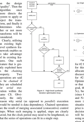
Optimisation proceeds through multiple repetitions of the optimisation loop shown in figure 4, and depends on the set of available transforms, a cost function reflecting designer requirements, and the controlling algorithm.
High-level synthesis transforms are typically related to allocation (e.g. sharing two hardware units) or scheduling (e.g. merging two control steps). In the current version of MOODS, roughly 20 transforms are available.
The whole optimisation process is controlled by a cost function of the form
n n a
c a c a c
Cost= 1× 1+ 2× 2+L+ × (1)
where :
aiare user specifications (typically n=3, and a1, a2, a3
correspond to area, delay and clock period)
ciare weight constants reflecting priorities (high or low)
It is through this function that a particular transform at a particular state of the design is characterised as beneficial or degrading.
Finally, all decisions that need to be taken during optimisation are made using a suitable algorithm. In MOODS, both simulated annealing and goal-oriented heuristics are currently available [8].
We are now able to explain the optimisation loop (figure 4). In the transform and data selection phase, the algorithm chooses a transform and suitable data. During the validity check phase, it is determined whether or not the transform can be applied at the given moment (several dependencies may prevent it). If the validity check succeeds, then the cost function is used during the cost
estimation phase to calculate the impact of the transform
Figure 2. Inversion Testing Comparator
Error
Module 1
Module 2 Functional
Output
Functional Input
1
2
3
+1
*2
-1 *1
A1
S1
M2 M1
Figure 3. Algorithmic
inversion:motivational
on the design “quality”. Then the algorithm once more directs the system to apply or reject the trans-form, and finally it determines whe-ther or not more transforms will be considered.
Clearly, utilising an existing high-level synthesis fra-mework enables us to take advantage of its existing fea-tures. One such feature that is gre-atly exploited here
is the chaining
property. Two operations are said to be chained if they are scheduled
for serial
exe-cution within the same CS. Obvi-ously, the only
reason why serial (as opposed to parallel) execution would be needed is data dependency. Chained operations are the result of merging associated (consecutive) control steps. When such merging is applied, steps are clearly saved, but the clock period may need to be lengthened, so that the series of operations can fit in a single step.
4. Versatile Implementation
As shown in section 3, optimisation within a system like MOODS relies on the following elements : transforms, the cost function and an algorithm. Therefore, to introduce a new functionality, one needs to define appropriate transforms to implement the functionality, provide a supplement to the cost function to reflect new concepts, and also choose an algorithm to automate the process.
4.1 On-line test insertion transforms
In order to include test resource insertion within the synthesis framework, three additional transforms have been implemented in about 2000 lines of C++ code (including test, estimate and perform functions for each). Two of the transforms implement test resource insertion (one for duplication and one for inversion), and the third one implements removal of (previously inserted) test resources. This last transform serves as an “undo” transform and is needed whenever a “step back and try an alternative route” approach is to be adopted.
Note that the resulting design immediately after test insertion is, once more, naïve; it is the subsequent optimisation steps that produce efficient designs. This is clarified in figure 5. Without loss of generality, we assume
that it is the du-plication testing scheme that is being applied. The original sta-te of part of a DFG is shown in 5a. Operations #1 and #2 (of the same kind) are scheduled for the same CS, N, and allocated to units C1 and C2 re-spectively. In 5b, duplication (#2´) and comparison (!=) operations for #2 have been inserted. Two new CSs have been added for this purpose, while the new operations have been allocated to new data path units. For the sake of the discussion we assume that the clock period is long enough for #2´ and != to be chained within a single CS. Optimisation can then proceed to either the situation of 5c or that of 5d. If hardware saving is the primary designer goal, then modules for #1 and #2´ will be shared (as in 5c), but an additional CS N+1 will have to be tolerated (since C1 is active during both N and N+1, therefore N and N+1 cannot be merged). Alternatively, if speed is more important than area, then we end up with the situation of 5d, where no CS needs to be added, but the price is the area of the additional module C3. Note that the decision regarding which of the two optimisation paths will be followed is taken automatically by the system, using eq. (1). Therefore, we have shown that our approach gives the designer the flexibility to choose between time or hardware redundancy, instead of imposing a particular strategy. Further, we have demonstrated a counter-intuitive result : a naïve start leads to a versatile process.
Finally, in order for the testing scheme to be valid, an operation and its duplicate cannot be assigned to the same unit (e.g. C2 and C3 in figure 5b must not be shared). For this purpose, the (existing) unit sharing transform test phase has been supplemented with appropriate checking.
4.2 A metric for on-line testability
Using the cost function (eq. (1)) with only its usual area and timing parameters, causes the test insertion transforms to look very expensive (since they are introducing both new units and new control steps, as seen in the transition from figure 5a to 5b). Therefore, eq. (1) needs to be expanded to reflect the benefit of our transforms, that is increased on-line testability. Using the terminology of section 3, n must take the value 4, and a metric a4for
on-line testability needs to be defined and included in (1), together with the appropriate weight c4. The following
expression is proposed as such a metric :
( )
[
( )
4]
1 3 1 2 2 1 1
4= =σ × +σ × ×1− +σ ×log +σ
−
− P P P L
T
a online (2)
where :
P1% is the percentage of operations made on-line testable
P2% is the average (per module) idle time availability transform
and data selection
execution validity test
cost estimation transformation
valid?
perform transformation?
perform another transformation?
yes
yes no
no no
yes
[image:3.595.61.339.67.471.2]end
Figure 4 : High-level synthesis iterative optimisation loop
optimisation loop
Figure 5. Introducing a testing scheme #2
#1 C1 C2 #1 C1 #2 C2
#2’ C3
!=
(a) Original state (b) Immediately after test resource insertion
#2 #1 C1 C2
(c) Optimising for area (d) Optimising for speed
#2 #1 C1 C2
!= #2’ C1
!= #2’ C3
N N
N+1
N+2
N
N
[image:3.595.270.541.71.508.2]L (measured in control steps) is the average (per
instruction) error latency*
σ1,σ2,σ3,σ4are constants
The first termσ1
×
P1signifies that the more the testableoperations within the design, the more testable the whole design is. The second termσ2
×
P2×
(1-P1) reflects the fact(because of P2) that designs with considerable idle time
will produce more compact on-line testable realisations. Therefore, in the first stages of optimisation (when P1→0)
the existence of idle time is an advantage; when most of the operations have been made on-line testable (therefore
P1→1), idle time is not needed anymore and this term
gradually comes out of play (because of 1-P1). As for the
third termσ3
×
[log(L-1)+σ4], it simply reflects the fact thatthe sooner the fault is detected the better.
Note that eq. (2) is ultimately normalised over its maximum value (obtained for P1=100% and L→0), and so
Ton-lineis expressed in %.
4.3 Algorithm
As mentioned in section 3, simulated annealing [8] is readily available within MOODS. Its advantage is generality (whatever can be quantified can also be optimised for); its drawback is low speed. Thus, fast area-or delay-area-oriented heuristics are also available [8]. In this work, we take advantage of the generic nature of simulated annealing to optimise for testability (that is, introduce on-line testing by means of the discussed transforms), and then use the heuristics to optimise for speed and / or area (as directed by designer goals).
5. Experimental results
In this section, we present the results of our experimentation. Three High-Level Synthesis Workshop benchmarks, namely tseng (1991), diffeq (1992) and qrs (1995), are used to illustrate our results.
5.1 Synthesis results
In all experiments, benchmarks have initially been synthesized behaviourally using the MOODS system. Subsequently, Synplicity Synplify Pro Version 6.2 has been used for RTL synthesis, while Xilinx Design Manager version 3.1i has been used for the final implementation. The results are shown in tables 1 – 8.
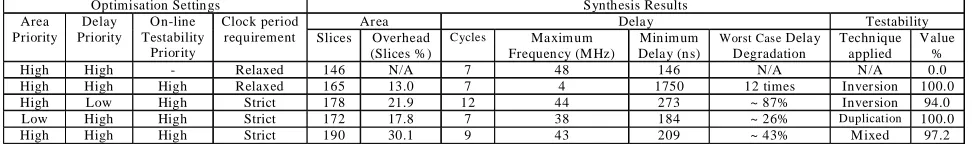
The first row of each of the tables corresponds to the untestable design, while the second, third and fourth (and fifth on table 1) rows show testable implementations produced using several combinations of user requirements. Area and performance penalties are reported with respect to the corresponding untestable design.
Designer priorities (regarding area, delay, on-line testability and clock period) for each particular experiment are given in the first four columns. Designer clock period requirements are reported on a scale of “relaxed” to “very strict”, where relaxed means that the period is long enough for the system to do as much chaining as possible,
*
The term error latency refers to the number of control steps that elapse between the occurrence and the detection of a fault.
while other classifications allow less and less chaining. In theory, allowing chaining is expected to lead to smaller realisations and fewer control steps, but low frequencies, while preventing chaining retains a high frequency value but gives rise to more control steps.
The next two columns report the area statistics of the corresponding designs (in FPGA slices), together with the associated area overhead percentage.
The next four columns show performance statistics. Number of clock cycles, maximum achievable frequency, minimum delay and the worst case delay degradation are all reported. Minimum delay is equal to (cycles / maximum frequency). That is, the reported values for the
worst case degradation reflect the degradation in delay
that would be suffered, if the designer required maximum frequency. To illustrate this point, let us refer to the second row of table 1. The total delay is reported to be degraded 12 times with respect to the corresponding untestable design. However, this only applies if the designer requires a maximum (48 MHz) frequency for the original design. If a lower value was enough for the untestable version, then the actual delay degradation would be much more tolerable. In other words, the reported delay degradation is as pessimistic as possible and the actual degradation can only be evaluated within the context of each particular application.
Finally, the last two columns report testability evaluation. This includes the applied testing technique* and the resulting testability value (calculated by eq. (2)). “Mixed” technique refers to cases where some operations are duplicated and some others inverted. All operations are made on-line testable; whenever testability is not 100%, this is due to non-zero error latency.
Table 1 shows synthesis results for the Tseng benchmark. In this small design, we can easily verify our predictions about the relationship between clock period requirements and design size. Indeed, the most compact on-line testable design in this case, is the one in the second row, which corresponds to relaxed period specification, leading to inversion testing and resulting in chains of the form (operation, inverse) executed serially within the same CS. A severe degradation in frequency is suffered (since there is data dependency between an operation and its inverse, as figure 2 shows). A much faster (yet somewhat bigger) realisation is that of the fourth row, where strict period specification leads to duplication (CS merging in a duplicated operation leads to insignificant frequency degradation, since an operation and its duplicate are scheduled to be executed in parallel). Even higher frequency values can be achieved. The third and fifth rows of the same table show such examples.
Tables 2 – 4 and 5 – 8 show our results for the more complicated Diffeq and Qrs benchmarks respectively. Because of increased complexity (especially in the Qrs case), the results do not reflect the relationships between design characteristics as clearly as in the previous case. Nevertheless, in tables 2 – 4, nine different self-checking realisations of Diffeq are presented, providing on-line testing for hardware overhead between 37.2% and 103.8%, in as few as 13 and as many as 30 clock cycles,
*
with a maximum frequency between 6 – 40 MHz, and a worst case delay degradation between 44% and 760%. Similarly, in tables 5 – 8, twelve self-checking realisations of the Qrs design can be found, providing on-line testing for a hardware overhead between 52.3% and 131%, in 31 – 144 clock cycles, with a maximum frequency between 0.8 - 7.1 MHz, and a worst case delay degradation of 65% - 1430%.
It is to be noted that all size and frequency values are those reported by the implementer tool. Therefore, they are the most realistic we can get, and they reflect all low level optimisations as well as the high-level ones.
Comparison of the achieved results with those of other approaches ([3, 4, 5, 6]) is hard to carry out, since RT and gate level synthesis in each case are performed by different tools and different technologies are targeted. In any case, though, the most important feature of our approach demonstrated in this section is not hardware savings or improved performance; rather, it is fast design
space exploration, with minimal designer effort (limited
to changing priority settings), provided by fully automating on-line test resource insertion within behavioural synthesis. Ultimately, it is the designer who makes the decision regarding which one of the realisations best accommodates his or her needs. None of them can be favoured or rejected in advance; each one can only be evaluated in the context of the project the design is part of. Further, even if a synthesis session fails to meet designer’s requirements (as is probably the case e.g. in the last row of table 8, where a hardware penalty of 131% and considerable delay penalty are reported), an alternative realisation can be obtained efficiently and painlessly, simply by changing a limited number of settings and repeating the session. As the tables show, much better results are very likely to be achieved (for example, row 3 of table 5 gives a hardware overhead of just 56.6%).
5.2 Simulation results
In order to verify that our implementations in fact detect system faults, we have conducted a number of fault injection and simulation experiments. We have been experimenting with the Tseng benchmark mentioned above, and we performed fault simulations using a variation of the transparent fault injection technique presented in [9]. In this method, the VHDL architecture of every RTL module is replaced by an alternative architecture, which includes structures to simulate faulty behaviour in the presence of each modelled fault.
The single stuck-at fault model is used. While this model is not “literally” valid in the on-line context (since any signal “physically” stuck at a value should have been detected during production test), it still provides a convenient way to emulate faulty behaviour. Therefore, it would be better to say that we simulated against defects whose effect can be modelled using stuck-at faults. Further, we targeted faults in data path units only, while the controller, interconnect, sto-rage, and “glue” logic parts are considered for the
time being to be fault free. Finally, introduced comparators are also for the purposes of the current state of our work regarded as fault free.
We simulated against random faults, for a variety of
random inputs. Thus, we imitated the behaviour of a
system for which we cannot know the functional inputs a priori. Table 9 shows our results. Masked faults refer to faults that do not corrupt module outputs; therefore they
should not be detected. Due to the fault secure nature of
duplication and invertion testing, we expect that all non-masked faults will be detected. Indeed, this is verified by the presented results.
6. Conclusions
In this paper, we have presented an integral, cost
function driven on-line test synthesis framework, which is
able to incorporate a variety of alternative algorithms and techniques. The three main contributions of this work are : - Insertion of self-checking resources does not require any modification of input HDL code, and it is part of the design optimisation process. This enables efficient and versatile design space exploration, while designs of realistic complexity can be made on-line testable with no additional designer effort. To the best of our knowledge, this issue is explicitly considered for the first time.
- A metric for on-line testability is proposed and used. We expect this concept to be useful in other cost function-driven systems.
- Inversion testing provides an additional degree of freedom to the system towards minimising overheads.
Current work involves replacing the conventional comparator modules currently used with fault secure [1] ones, and modifications to the existing system to accommodate them.
7. References
[1] M. Nicolaidis, L. Anghel, “Concurrent Checking for VLSI”, Microelectronic Engineering, Vol. 49, No. 1-2, November 1999, p. 139-156.
[2] S. Mitra, E.J. McCluskey, “Which concurrent error detection scheme to choose?”, IEEE International Test Conference, 2000, p. 985-994.
[3] A. Orailoglu, R. Karri, “Automatic Synthesis of Self-Recovering VLSI Systems”, IEEE Transactions on Computers, Vol. 45, No. 2, February 1996, p. 131-142.
[4] K. Wu, R. Karri, “Exploiting Idle cycles for Algorithm Level Re-Computing”, Design Automation and Test in Europe (DATE) 2002, p. 842 – 846.
[5] R. Karri, B. Iyer, “Introspection : A Register Transfer Level Technique for Concurrent Error Detection and Diagnosis in Data Dominated Designs”, ACM Transactions on Design Automation of Electronic Systems, Vol. 6, No. 4, October 2001, p. 501-515. [6] A. Antola, F. Ferrandi, V. Piuri, M. Sami, “Semiconcurrent
Error Detection in Data Paths”, IEEE Transactions on
Computers, Vol. 50, No. 5, May 2001, p.449-465.
[7] P. Oikonomakos, M. Zwolinski, “Using High-Level Synthesis to Implement On-Line Testability”, IEEE/IEE Real-Time Embedded Systems Workshop, 2001.
[8] A.C. Williams, “A Behavioural VHDL synthesis system using data path optimisation”, PhD Thesis, University of Southampton, 1997.
[9] M. Zwolinski, “Digital System Design with VHDL”, Prentice Hall, 2000.
faults
injected masked detected escaped 100000 65912 34088 0
Optimisation Settin gs Synth esis Results
Area Delay Testability Area
Priority Delay Priority
On-line Testability
Priority
Clock period
requirement Slices Overhead (Slices %)
Cycles Maxim um Frequen cy (MHz)
Min im um Delay (n s)
Worst CaseDelay Degradation
Techn ique applied
Value % High High - Relaxed 146 N/A 7 48 146 N/A N/A 0.0 High High High Relaxed 165 13.0 7 4 1750 12 times Inversion 100.0 High Low High Strict 178 21.9 12 44 273 ~ 87% Inversion 94.0
[image:6.595.57.544.67.140.2]Low High High Strict 172 17.8 7 38 184 ~ 26% Duplication 100.0 High High High Strict 190 30.1 9 43 209 ~ 43% Mixed 97.2
TABLE 1 : Tseng Benchmark Synthesis Results (Target Technology Xilinx XCV800)
Optim isation Settin gs Synth esis Results
Area Delay Testability Area
Priority Delay Priority
On -lin e Testability
Priority
Clock period
requirement Slices Overhead (Slices %)
C ycles Maximum Frequency (MHz)
Min im um Delay (n s)
Worst CaseDelay Degradation
Technique applied
Value % High High - Relaxed 234 N/A 13 31 419 N/A N/A 0.0 High High High Relaxed 321 37.2 14 6 2333 5.5 tim es Inversion 100.0 High Low High Relaxed 327 39.7 13 7 1857 4.4 tim es Inversion 100.0 Low High High Relaxed 321 37.2 14 8 1750 4.2 tim es Inversion 100.0
TABLE 2 : Diffeq Benchmark Synthesis Results (Target Techn ology Xilinx XCV800, Relaxed Clock Period Requirement)
Optim isation Settin gs Synth esis Results
Area Delay Testability Area
Priority Delay Priority
On -lin e Testability
Priority
Clock period
requirement Slices Overhead (Slices %)
C ycles Maximum Frequency (MHz)
Min im um Delay (n s)
Worst CaseDelay Degradation
Technique applied
Value % High High - Moderate 234 N/A 13 31 419 N/A N/A 0.0 High High High Moderate 477 103.8 20 7 2857 6.8 tim es Mixed 94.3 High Low High Moderate 418 78.6 19 6 3167 7.6 tim es Inversion 94.3 Low High High Moderate 425 81.6 19 28 679 ~ 62% Duplication 94.3
TABLE 3 : Diffeq Bench mark Syn thesis Results (Target Techn olog y Xilinx XCV800, Moderate Clock Period Requirem ent)
Optim isation Settin gs Synth esis Results
Area Delay Testability Area
Priority Delay Priority
On -lin e Testability
Priority
Clock period
requirement Slices Overhead (Slices %)
C ycles M aximum Frequency (M Hz)
Min im um Delay (n s)
Worst CaseDelay Degradation
Technique applied
[image:6.595.60.540.429.496.2]Value % High High - Strict 306 N/A 19 42 452 N/A N/A 0.0 High High High Strict 424 38.6 29 34 853 ~ 88% M ixed 91.4 High Low High Strict 426 39.2 30 39 769 ~ 70% Inversion 91.2 Low High High Strict 422 37.9 26 40 650 ~ 44% Duplication 92.1
TABLE 4 : Diffeq Benchmark Synthesis Results (Target Technology Xilinx XCV800, Strict Clock Period Requirem ent)
Optim isation Settin gs Synth esis Results
Area Delay Testability Area
Priority Delay Priority
On -lin e Testability
Priority
Clock period
requirement Slices Overhead (Slices %)
C ycles M aximum Frequency (M Hz)
Min im um Delay (us)
Worst CaseDelay Degradation
Technique applied
Value % High High - Relaxed 470 N/A 34 3.1 11 N/A N/A 0.0 High High High Relaxed 738 57.0 31 1.0 31 2.8 tim es M ixed 98.7
Low High High Relaxed 736 56.6 31 0.8 39 3.5 tim es M ixed 97.9 High Low High Relaxed 947 101.5 99 7.1 14 1.3 tim es M ixed 92.7
TABLE 5 : Qrs Ben chmark Synthesis Results (Target Technolog y Xilin x XCV1000, Relaxed Clock Period Requirement)
Optim isation Settin gs Synth esis Results
Area Delay Testability Area
Priority Delay Priority
On -lin e Testability
Priority
Clock period
requirement Slices Overhead (Slices %)
C ycles M aximum Frequency (M Hz)
Min im um Delay (us)
Worst CaseDelay Degradation
Technique applied
Value % High High - Moderate 457 N/A 34 8.7 4 N/A N/A 0.0 High High High Moderate 780 70.7 36 0.9 40 10 tim es M ixed 96.6
Low High High Moderate 770 68.5 36 1.2 30 7.5 tim es M ixed 96.3 High Low High Moderate 904 97.8 96 5.3 18 4.5 tim es M ixed 93.1
TABLE 6 : Qrs Ben chmark Synthesis Results (Target Technology Xilin x XCV1000, Moderate Clock Period Requirement)
O p tim isa tion S e ttin gs S yn th esis R e sults
A r ea D ela y T esta bility
A re a P riority
D e la y P riority
O n -lin e T esta bility
P rior ity
C loc k pe riod
req u irem e nt S lice s O ve r h e a d (S lice s % )
C ycle s M a xim u m F r e qu en cy (M Hz )
M in im um D ela y (u s)
W or st C as eD ela y D eg ra da tion
T ec hn iq ue a p plied
V a lue % H igh H igh - S trict 5 1 4 N /A 4 5 2.6 17 N /A N /A 0 .0 H igh H igh Hig h S trict 8 4 4 64 .2 5 0 1.3 38 2 .2 tim es M ixe d 94 .8
L ow H igh Hig h S trict 7 8 3 52 .3 4 9 1.4 35 2 .1 tim es D u p licat ion 95 .2 H igh L ow Hig h S trict 9 2 7 80 .4 10 2 3.7 28 ~ 6 5% M ixe d 92 .9
T A B L E 7 : Qrs B en ch m a rk S yn th e sis R esu lts (T ar ge t T e ch n olog y X ilin x X C V 1 0 00, S trict C loc k P eriod R eq u ire m e nt)
O p tim isa tion S e ttin gs S yn th esis R e sults
A r ea D ela y T esta bility
A re a P riority
D e la y P riority
O n -lin e T esta bility
P rior ity
C loc k pe riod
req u irem e nt S lice s O ve r h e a d (S lice s % )
C ycle s M a xim u m F r e qu en cy (M Hz )
M in im um D ela y (u s)
W or st C as eD ela y D eg ra da tion
T ec hn iq ue a p plied
V a lue % H igh H igh - V ery S trict 5 6 4 N /A 6 6 1 9. 2 3 N /A N /A 0 .0 H igh H igh Hig h V ery S trict 1 17 8 10 8 .9 9 6 3.9 25 8 .3 tim es M ixe d 92 .3
L ow H igh Hig h V ery S trict 1 17 8 10 8 .9 7 8 1.8 43 14 .3 tim e s D u p licat ion 92 .7 H igh L ow Hig h V ery S trict 1 30 3 13 1 .0 14 4 4.4 33 1 1 tim e s M ixe d 91 .2