International Journal of Engineering
J o u r n a l H o m e p a g e : w w w . i j e . i rHarmonic Reduction Technique Using Flying Capacitor Based Z Source Inverter for
a DVR
S. Deepa a, S. Rajapandian b*
a Research Scholar, Sathyabama University, Chennai, India. b Panimalar Engineering College, Chennai, India
P A P E R I N F O
Paper history: Received 20 May 2012
Received in revised form 10 October 2012 Accepted15 November 2012
Keywords:
DVR
Z-Source Converter Flying Capacitor Voltage Sag Power Quality
A B S T R A C T
The Dynamic Voltage Restorer (DVR) is a commercially available, popular device to eliminate voltage sags and swells in the distribution lines. Its basic function is to inject the voltage difference (difference between the pre-sag and sag voltage) to the power line and maintains the pre-sag voltage condition in the load side. The efficiency of the DVR depends on the performance of the efficiency control technique involved in switching the inverters. Z-source inverters are recent topological options proposed for buck–boost energy conversion with a number of possible voltage- and current-type circuitries. Common feature noted is their inclusion of an LC impedance network, placed between the dc input source and inverter bridge. This impedance network allows the output end of a voltage-type Z-source inverter to be shorted for voltage boosting without causing a large current flow and the terminal current of a current-type inverter to be interrupted for current boosting without introducing over voltage oscillations to the system. Therefore, Z-source inverters are, in effect, safer and less complex and can be implemented using only passive elements with no additional active semiconductor needed. This paper presents a selective harmonic elimination using flying capacitor connection in Z-source inverter. Closed loop control for a simple system is modeled and simulated using MATLAB software. The simulation results are presented to demonstrate the effectiveness of the proposed DVR system.
doi: 10.5829/idosi.ije.2013.26.03c.11
1. INTRODUCTION1
The need of the electrical power is increasing and simultaneously the problems while transmitting the power through the distribution system are also increasing. Voltage fluctuations are considered as one of the most severe power quality disturbances to be dealt with. Even a short-duration voltage fluctuation could cause a malfunction or a failure of a continuous process. There are several types of voltage fluctuations that can cause the systems to malfunction, including surges and spikes, sag, swell, harmonic distortions, and momentary disruptions. Among them, voltage sag and swell are the major power quality problems. Voltage swell is the sudden increase of voltage to about more than 110% amplitude of the supply voltage, whereas the voltage sag is the sudden decrease of voltage ton about 90%amplitude of supply voltage. This is caused due to
*Corresponding Author Email: [email protected] (S.
Deepa)
the sudden reduction or addition of the load across that particular feeder. This change of voltage is compensated by injecting the voltage in series with the supply from another feeder at the time of disturbances using DVR. Electronics devices hold substantial promise for making distributed energy applications more efficient and cost effective.
toward connecting small power resources to the medium and low voltage network [2]. Power quality standards for connection of an inverter to the grid are still under development, since previously there have been a few similar high power applications. In [3] it is stated that the power quality is determined by the voltage quality, when the voltage is a controlled variable. In order to deliver a good ac power the controlled pulse width modulation (PWM) inverter and L-C output filter have to convert a dc voltage source (e.g. batteries) to a sinusoidal ac voltage with low voltage THD and fast transient response under load disturbances.
Another important aspect of power quality is harmonic distortion. General requirements for harmonic distortion can be found in standard [4] and particularly for connection of distributed resources to grid in [4]. PWM control is the most powerful technique that offers a simple method for control of analog systems with the processor's digital output [5]. With the availability of low cost high performance DSP chips characterized by the execution of most instructions in one instruction cycle, complicated control algorithms can be executed with fast speed, making very high sampling rate possible for digitally-controlled inverters [6]. The Z-source inverter, utilizing a unique LC network and previously forbidden shoot-through states, provides unique features, such as the ability to buck and boost voltage with a simple single stage structure The Z-source inverter exhibits new operation modes that have not been discussed before. This analyzes these new operation modes and the associated circuit characteristics [7]. Depending upon the boosting factor capability of impedance network the rectified DC voltage is buck or boost upto the voltage level of the inverter section (not exceed to the DC bus voltage). This network also acts as a second order filter and it should be required less number of inductor and capacitorc [8, 9]. In this paper, the modeling and control of voltage sag/swell compensation using new control technique based dynamic voltage restorer are simulated using MATLAB software. The simulation results are presented to show the effectiveness of the proposed control method.
2. DYNAMIC VOLTAGE RESTORERS
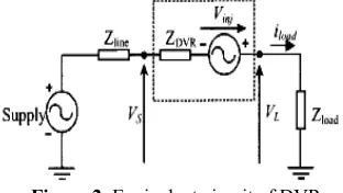
A DVR is a device that injects a dynamically controlled voltage Vinj(t) in series to the bus voltage by means of a booster transformer as depicted in Figure 1. The amplitudes of the injected phase voltages are controlled such as to eliminate any detrimental effects of a bus fault to the load voltage VL(t). This means that any differential voltage caused by transient disturbances in the AC feeder will be compensated by an equivalent voltage generated by the converter and injected on the medium voltage level through the booster transformer.
The DVR works independent of the type of fault or any event that happens in the system, provided that the whole system remains connected to the supply grid, i.e. the line breaker does not trip. For most practical cases, a more economical design can be achieved by only compensating the positive and negative sequence components of the voltage disturbance seen at the input of the DVR. This option is reasonable because for a typical distribution bus configuration, the zero sequence part of a disturbance will not pass through the step down transformers because of infinite impedance for this component. For most of the time, the DVR has virtually, "nothing to do," except monitoring the bus voltage. This means it does not inject any voltage (Vinj(t)= 0) independent of the load current. Therefore, it is suggested to particularly focus on the losses of a DVR during normal operation. Two specific features addressing this loss issue have been implemented in its design, which are a transformer design with low impedance, and the semiconductor devices used for switching Mathematically expressed, the injection satisfies
VL(t) =Vs(t)+Vinj(t) (1)
where, VL(t) is the load voltage, Vs(t) is the sagged supply voltage and Vinj(t) is the voltage injected by the mitigation device as shown in Figure 2. Under nominal voltage conditions, the load power on each phase is given by
S L = ILVL* = PL - jQL (2)
where, I is the load current, and, PL and QL are the active and reactive power taken by the load respectively during a sag.
Figure 1. Schematic diagram of DVR System
When the mitigation device is active and restores the voltage back to normal, the following applies to each phase
SL =PL-j QL=(PS-j Qs) +(Pinj-jQinj) (3) where, the sag subscript refers to the sagged supply quantities. The inject subscript refers to quantities injected by the mitigation device.
The real and reactive power is given by
Pp=|Vp|
å
=n
q 1
|Vq|(Gpq Cosdpq + Bpq Sindpq) (4)
Qp=|Vp|
å
=n
q 1
|Vq|(GpqSindpq - BpqCosdpq) (5)
3. Z-SOURCE INVERTER
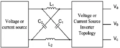
Z-source inverter has X-shaped impedance network on its DC side, which interfaces the source and inverter H-bridge. It facilitates both voltage-buck and boost capabilities. The impedance network composed of split inductors and two capacitors. The supply can be DC voltage source or DC current source or AC source. Z-source inverter can be of current or voltage Z-source type Z-Source inverter operation is controlled by multiple pulse width modulation. The output of the Z-Source inverter is controlled by using pulse width modulation, generated by comparing a triangular wave signal with an adjustable DC reference. Hence, the duty cycle of the switching pulse could be varied to synthesize the required conversion. A stream of pulse width modulation is produced to control the switch as shown in the Figure 4.
In single-phase Z-Source inverter has five switching modes. Two active modes in which the dc source, voltage is applied to load, two zero modes in which the inverter’s output terminals are short circuited by S1 and
S3 or S2 and S4 switches and a shoot-through mode which occurs as two switches on a single leg are turned on. In a symmetric impedance network, the following equations are valid:
C1 = C2 = C (6)
L1 = L2 = L (7)
V C1 = V C2 = VC (8)
The voltage of capacitors in a symmetric impedance network is as follows:
Vi = β Vdc (9)
β = 1 / [1 – 2(T0/T)] (10)
where, T0 and T show the shoot-through mode application period and switching period, respectively. F Furthermore, the following relation is valid in symmetric impedance networks:
Vi = 2VC –Vdc (11)
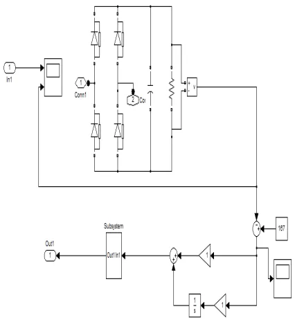
It should be noted that the relations mentioned above are extracted by averaging the ZSI operational modes. The shunt full bridge rectifier with the input capacitor Ce which feeds the impedance network is shown in Figure 6. During the commutation between diodes, it is possible to face with surge voltage due to line inductance and shoot-through mode operation. The input capacitor is used to suppress this surge voltage. Diodes D1and D4are turned on if the input voltage of rectifier is positive. Diodes D3 and D2 are turned on if the input voltage of rectifier is not positive.
Figure 3. General Block Diagram of Z-Source Inverter
Figure 4. Multiple Pulse Width Modulation
Figure 6. Active modes
Figure 7. Voltage Sag Compensation in a DVR System
Figure 8. Subsystem 1 of Closed Loop Control of Voltage Sag Compensation in a DVR System
The equivalent circuits of rectifier fed ZSI in shoot-through and active modes are presented in Figures 5 and 6, respectively. The following is obtained according to that equivalent circuit:
Vd = VL1 +VC2 (12)
VL1 =VC1 (13)
where, Vd is the impedance network input voltage.
4. VOLTAGE SAG COMPENSATION IN DVR SYSTEM
The performance of the designed DVR as shown in Figures 7 and 8 is evaluated using Matlab/Simulink. The proposed method was tested for voltages sag in the low voltage distribution system.
In case of voltage sag, the source voltage has decreased about 20-25% of its nominal value. It shows the grid voltage which has dropped to 25% at t=0.3 sec and the sag lasts 0.7 sec and then voltage will restore back to its normal value. The function of the DVR will injects the missing voltage in order to regulate the load voltage from any disturbance due to immediate distort of source voltage.
Figure 8 shows the subsystem 1 of the closed loop DVR system. It contains the PI controller. The AC output voltage is rectified to DC supply and then a reference voltage is given for the error. This error is sent to the PI controller. The saturator value is given as pulses for controlling the Z-Source inverter.
In the Figure 9, subsystem 2 contains the Z-Source inverter which is being controlled by the PI controller. The Z-Source starts conducting when it obtains the pulse from the saturator. The selected value of switching frequency of PWM is 5 kHz. It has a dynamic response timeof about one cycle. The parameters of PI controller are selected based on conventional method. The reference for firing angle is zero. Figure 10 shows the output waveform of closed loop control of voltage
sag compensation. Figure 10(a) shows the
uncompensated AC voltage with 25% sag. Figure 10(b) shows the injected DVR voltage. Figure 10(c) gives the compensated output voltage.
Figure 9. Subsystem 2 of Closed Loop Control of Voltage Sag Compensation in a DVR System
Figure 10. Simulation results of Closed Loop Control DVR with 30% swell (a.)Uncompensated Voltage(b). Injected DVR Voltage (c). Compensated Voltage
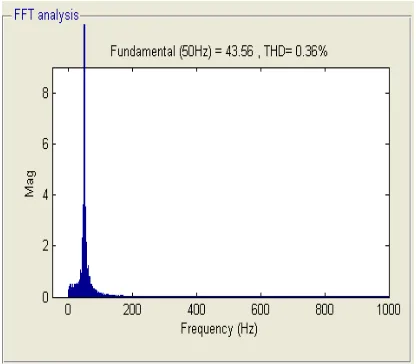
Figure 11. FFT analysis for firing angle α=60
TABLE 1. Voltage harmonics for different values of firing angle (α)
α Degree
THD Harmonic
eliminated order n Conventional
method (%)
Proposed method (%)
25.5 1.52 0.13 7th
36 1.48 0.25 5th
60 1.89 0.36 3rd
5. CONCLUSION
The power quality problems related to voltage sag and swell are presented in this paper. The transient models of custom power equipment, namely, DVR and IDVR were presented and applied to the study of power quality. From the simulation results the following conclusions are drawn:
· The DVR compensates the disturbance caused by sag and swell effectively while utilizing the stored energy fully with the use of buck-boost capability of the proposed Z-source inverter.
· The proposed Z source inverter is a viable alternative to conventional inverters, since it can boost the input voltage and control the short circuit current.
· Load voltage compensation results in maintaining the system voltage at the normal level.
· The proposed impedance source inverter based DVR is found to produce the lowest harmonics.
· The simulation results validate that the implemented control strategy compensates the voltage sag and swell with high accuracy.
6. REFERENCES
1. Wang, B., Venkataramanan, G. and Illindala, M., "Operation and control of a dynamic voltage restorer using transformer coupled H-bridge converters", IEEE Transactions on Power Electronics, Vol. 21, No. 4, (2006), 1053-1061.
2. Goharrizi, A. Y., Hosseini, S. H., Sabahi, M. and Gharehpetian, G. B., "Three-Phase HFL-DVR With Independently Controlled Phases", IEEE Transactions on Power Electronics, Vol. 27, No. 4, (2012), 1706-1718.
3. Barros, J. D. and Silva, J. F., "Multilevel optimal predictive dynamic voltage restorer", IEEE Transactions on Industrial Electronics, Vol. 57, No. 8, (2010), 2747-2760.
4. Nguyen, P. and Saha, T., "DVR against balanced and unbalanced Voltage sags: Modeling and simulation", IEEE-School of Information Technology and Electrical Engineering, University of Queesland, Australia, (2004).
5. Chung, Y., Won, D.-J., Park, S.-Y., Moon, S.-I. and Park, J.-K., "The DC lin energy control method in dynamic voltage restorer system", International Journal on Electric Power and Energy System, Vol. 25, No. 7, (2003), 525-531.
Power Electronics and ECCE Asia (ICPE & ECCE), 8th International Conference on, IEEE, (2011), 1843-1847. 7. Rabi, B. J. and Arumugam, R., "Harmonics study and
comparison of Z-source inverter with traditional inverters",
American Journal of Applied Sciences, Vol. 2, No. 10, (2005), 1418-1426.
8. Shen, M., Joseph, A., Wang, J., Peng, F. Z. and Adams, D. J., "Comparison of traditional inverters and Z-source inverter for
fuel cell vehicles", IEEE Transactions on Power Electronics,
Vol. 22, No. 4, (2007), 1453-1463.
9. Ibrahim, A. O., Nguyen, T. H., Lee, D. C. and Kim, S. C., "A fault ride-through technique of DFIG wind turbine systems using dynamic voltage restorers", IEEE Transactions on Energy Conversion, Vol. 26, No. 3, (2011), 871-882.
Harmonic Reduction Technique Using Flying Capacitor Based Z Source Inverter for
a DVR
S. Deepa a, S. Rajapandian b
a Research Scholar, Sathyabama University, Chennai, India. b Panimalar Engineering College, Chennai, India
P A P E R I N F O
Paper history: Received 20 May 2012
Received in revised form 10 October 2012 Accepted15 November 2012
Keywords: DVR Z-Source Converter Flying Capacitor Voltage Sag Power Quality هﺪﯿﮑﭼ هﺎﮕﺘﺳد نادﺮﮔﺮﺑ ژﺎﺘﻟوﯽﮑﯿﻣﺎﻨﯾد ) DVR ( ، ﻪﮐ
سﺮﺘﺳدرديرﺎﺠﺗترﻮﺻﻪﺑ
ﺪﺷﺎﺑﯽﻣ
ندﺮﺑﻦﯿﺑزاياﺮﺑ تﺎﻧﺎﺳﻮﻧ
ردژﺎﺘﻟو
ﻊﯾزﻮﺗطﻮﻄﺧ
دﺮﯿﮔﯽﻣراﺮﻗهدﺎﻔﺘﺳادرﻮﻣ
.
ژﺎﺘﻟوفﻼﺘﺧاﻖﯾرﺰﺗياﺮﺑﻪﮐﺖﺳاﻦﯾانآﯽﻠﺻادﺮﮑﻠﻤﻋ
)
ﻦﯿﺑتوﺎﻔﺗ
دﺎﯾزوﻢﮐ
نﺪﺷ و ژﺎﺘﻟ
(
زاﻞﺒﻗژﺎﺘﻟوﺖﯿﻌﺿوﻆﻔﺣوترﺪﻗﻂﺧﻪﺑ
نﺎﺳﻮﻧ ﺪﺷﺎﺑﯽﻣرﺎﺑ
. يروهﺮﻬﺑ DVR ﻪﺑﯽﮕﺘﺴﺑ هدزﺎﺑ شور يﺎﻫ لﺮﺘﻨﮐ هدﺎﻔﺘﺳادرﻮﻣ رد لﺪﺒﻣ ﮓﻨﯿﭽﯿﺋﻮﺳ دراد . لﺪﺒﻣ Z
-ﺮﯿﺧاﮏﯾژﻮﻟﻮﭘﻮﺗﻪﻨﯾﺰﮔﻊﺒﻨﻣ ا
هﺪﺷدﺎﻬﻨﺸﯿﭘ ، كﺎﺑيژﺮﻧاﻞﯾﺪﺒﺗياﺮﺑ
-ﺖﺳﻮﺑ ، ﻧﺎﯾﺮﺟوژﺎﺘﻟوزايداﺪﻌﺗﺎﺑ
يراﺪﻣيﺎﻬ
ﭘنﺎﮑﻣا
ﺖﺳاﺮﯾﺬ
.
يﺎﻫﯽﮔﮋﯾوزا
ﯽﻠﮐ هﺪﺷﺮﮐذ ﺖﯿﻓﺮﻇ، ﻪﮑﺒﺷ LC ﺲﻧاﺪﭙﻣا ﻪﮐ،ﺖﺳا
يدوروﻊﺒﻨﻣﻦﯿﺑ
DC هﺪﺷهدادراﺮﻗﻞﭘﺮﺗرﻮﻨﯾاو ﺖﺳا
.
ﺎﺗﺪﻫدﯽﻣهزﺎﺟاﺲﻧاﺪﭙﻣاﻪﮑﺒﺷﻦﯾا يﺎﻬﺘﻧا زاﯽﺟوﺮﺧ عﻮﻧ لﺪﺒﻣ ﻊﺒﻨﻣ ژﺎﺘﻟو -Z ياﺮﺑ، ژﺎﺘﻟوﺖﯾﻮﻘﺗ نوﺪﺑ دﺎﺠﯾا ﮏﯾ نﺎﯾﺮﺟ گرﺰﺑ و لﺎﻨﯿﻣﺮﺗ زا ﺮﺗرﻮﻨﯾاعﻮﻧ هﺎﺗﻮﮐلﺎﺼﺗا هدﺮﮐ و ياﺮﺑ ﺶﯾاﺰﻓا ناﻮﺗ نﺎﯾﺮﺟ و دﺎﺠﯾا تﺎﻧﺎﺳﻮﻧ ،ژﺎﺘﻟوﻪﻨﯿﺸﯿﺑ ﺐﺟﻮﻣ ﻊﻄﻗ نﺪﺷ ﻢﺘﺴﯿﺳ ددﺮﮕﻧ . ،ﻦﯾاﺮﺑﺎﻨﺑ ﺮﺗرﻮﻨﯾا Z -،ﻊﺒﻨﻣ ،ﺮﺗﺮﺛﻮﻣ ﻦﻣا ﺮﺗ و هدﻮﺑﺮﺗهدﺎﺳ و ﺎﻬﻨﺗ ﺎﺑ هدﺎﻔﺘﺳا زا ﺮﺻﺎﻨﻋ وﻞﻌﻔﻨﻣ
ﻪﺑزﺎﯿﻧنوﺪﺑ ﻪﻤﯿﻧ يدﺎﻫ يﺎﻫ ﯽﻓﺎﺿا ﻞﺑﺎﻗ اﺮﺟا ﺖﺳا . رد ﻦﯾا ﻪﻟﺎﻘﻣ فﺬﺣ ﺎﻫ ﮏﯿﻧﻮﻣرﺎﻫي ﯽﺻﺎﺧ ﺎﺑ هدﺎﻔﺘﺳا زا تﻻﺎﺼﺗا نزﺎﺧ لﺪﺒﻣ Z
-ﺖﺳاهﺪﺷﻪﺋاراﻊﺒﻨﻣ
. لﺮﺘﻨﮐ ﻪﻘﻠﺣ ،ﻪﺘﺴﺑ ياﺮﺑ ﮏﯾ ﻢﺘﺴﯿﺳ ،هدﺎﺳ ﺎﺑ هدﺎﻔﺘﺳا زا مﺮﻧ ﺐﻠﻄﻣراﺰﻓا لﺪﻣ يزﺎﺳ و ﻪﯿﺒﺷ يزﺎﺳ ﺖﺳاهﺪﺷ . ﺞﯾﺎﺘﻧ ﻪﯿﺒﺷ يزﺎﺳ ياﺮﺑ نﺎﺸﻧ نداد ﯽﺸﺨﺑﺮﺛا ﻢﺘﺴﯿﺳ DVR ﻪﺋارا هﺪﺷ ﺖﺳا .