Please cite this article as: V. Shukla, A. Jain,Design of AWG based Optical Switch for High Speed Optical Networks, International Journal of Engineering (IJE), TRANSACTIONSA: Basics Vol. 29, No. 7, (July 2016) 909-915
International Journal of Engineering
J o u r n a l H o m e p a g e : w w w . i j e . i rDesign of Arrayed Waveguide Grating based Optical Switch for High Speed Optical
Networks
V. Shukla*, A. Jain
Department of Computer Science and Engineering, Birla Institute of Technology, Mesra ,Ranchi, India
P A P E R I N F O
Paper history:
Received 05 March 2016
Received in revised form 20 April 2016 Accepted 02 June 2016
Keywords: Optical Packet Switch Bit Error Rate PLR and Average Delay Arrayed Waveguide Grating
A B S T R A C T
This paper demonstrates the design of an Arrayed Waveguide Gratings (AWG) based optical switch. In the design both physical and network layer analysis is performed. The physical layer power and noise analysis is done to obtain Bit Error Rate (BER). This has been found that at the higher bit rates, BER is not affected with number of buffer modules. Network layer analysis is done to obtain performance in terms of packet loss rate and average delay. Analysis presented in the paper clearly reveals that there is a minimum amount of power required, which is necessary for the satisfactory performance of switch both at physical and network layer.
doi: 10.5829/idosi.ije.2016.29.07a.04
1. INTRODUCTION1
For the present internet communication infrastructure optical network is becoming an important aspect due to the huge bandwidth provided by the optical fiber. Optical fiber cables are used today for more than 80 percent of the world's long-distance communication. It is envisaged that, in all-optical network, buffering, switching and routing within the network nodes will be performed optically; while traffic at the backbone network will remain in optical domain. Network elements such as optical add/drop multiplexers and optical cross-connects will have full control on all wavelengths. They are expected to have full knowledge of the status of each wavelength and the traffic carrying capacity [1-4]. The main problem in such all-optical network is the unavailability of optical RAM and technology is not matured for optical processing.
Packet switching is an appropriate switching technique in all-optical network rather than circuit switching because of inefficient bandwidth utilization and is less costly in maintaining a circuit. Different contention resolution techniques are proposed which try to resolve contention.
1*Corresponding Author’s Email: [email protected] (V.
Shukla)
Optical buffers combining with tunable wavelength converters (TWCs), fiber delay lines can solve bottlenecks in limitations of optical switching.
The performance evaluation of the switches can be done both at physical as well as network layer [5-8]. Physical layer analysis is crucial in designing the basic parameters like switch size and buffering conditions. Parameter like packet loss probability is used to measure performance of the switch in network layer. For efficient switching high throughput is desired therefore low packet loss probability is to be achieved. In the physical layer, effects of system impairment on bit-error rate (BER) are studied.
2. RELATED WORK
Optical packet switch is considered as viable options for high speed data transfer and in optical data centers. For realizing on demand high bandwidth connectivity between top of rack switches; Proteus [10, 11] uses wavelength selective switch modules and optical circuit switches. For designing large switch matrix, Petabit [12] uses low radix AWG routers and tunable wavelength convertors. In the recent development [13, 14], Hy Scale (hybrid optical network based scalable switch centric architectures) is a switch centric recursively defined network that uses both optical burst switching and optical circuit switching. The switch proposed in [15] is a high speed switch, which uses TWCs and AWG to switch packets optically while buffering contending packets in a single shared electronic buffer.
In previous research ye et al. [16] performs a comparison between single wavelength fiber delay lines and electronic buffer in the context of AWG switch. In [9, 17-20], AWG based optical switch architectures are proposed with various buffer and SOA placements combinations. In [21], a hybrid optical/electronic buffering scheme and a method for efficiently integrating fiber delay line buffer capacity into the AWG wavelength assignment scheme. However, in this design O/E and E/O conversion is necessary to write and readout of the packets and may be good for data centres but not for optical switching.
In the similar directions, H. Rastegarfar [22] proposed a switch in which recirculating FDLs are used for storing the contending packets. In the switch, the packets which feel contention are directed towards recirculating FDL ports for buffering and when the contention is resolved then these packets are forwarded in the direction of output port fiber.
This switch has number of limitations which some of them are discussed as below:
The main advantage of WDM is lost; here by using the routing pattern of AWG N=32 packets can be stored in a single piece of fiber.
The another major limitation of switch is that the switch stores total of N packets in the buffer while on the other hand the proposed switch can stored, maximum of N2 packets.
In [23], authors also state that the packets remains in the buffer unit for single recirculation, then in such scenario what is the use of recirculating buffer?
This paper discusses an AWG based design. Power budget analysis is done, to evaluate the BER at the output of the switch under various power levels. This paper, also discusses how the, size of the packet and bit rate affects the BER performance of the switch. How the number of buffer modules affects the performance in terms of BER. To evaluate the performance of the switch at the network level, packet loss performance and average delay is performed, and results are compared with recently published design.
3. SWITCH DESIGN AND ANALYSIS
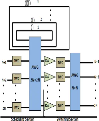
In the architecture (Figure 1), switch is divided in the scheduling and switching section. The scheduling section contains the TWCs, one 2N×2N AWG router, FDL lines for buffering of packets, and the switching section contains TWCs and an N×N AWG router [23]. The upper ‘N’ ports of scheduling AWG are connected to the ‘N’ FDL buffer modules. The other ports (N+1 to 2N) are actual input output ports. The input ports are equipped with the tunable wavelength converters (TWCs), and these TWCs are used to tune the wavelength of incoming packets as per the requirement of output packets. Suppose a packet arriving at input ‘i’ and destined to the output ‘j’ with required amount of delay of ‘k’ time slots then the packet is routed to the kth buffer module. To do so, the wavelength of the incoming packet is tuned as per the routing pattern of the cyclic AWG,
( , )i k l
, l [1 (i k 2) modN] (1)
The packet which is deflected through kth buffer module will again re-appear after the delay of ‘k’ time slots at the input port of scheduling AWG and due to the symmetric nature of scheduling AWG the packet get routed to the output port ‘i’ of the scheduling AWG. Finally, the packet is forwarded towards the appropriate output ‘j’ by tuning wavelength appropriately in the switching section.
3. 1. Physical Layer Analysis (Power Budget) 3. 1. 1. Power Analysis The loss in the power when
packet passes through the switch is:
N N AWG TWC N N AWG FDL N N AWG
TWCL L L L L
L 2 2 2 2
To fully compensate the loss, the gain of the SOA placed at the input of the switching AWG must satisfy.
2N 2N 2N 2N N N 1 TWC AWG FDL AWG TWC AWG
L L L L L L G
Power entering in the switch is:
[0,1]
s in
P bP b (2)
.The extinction ratio (ε = P0/P1) is assumed to be zero. Power at the output of the switch is:
3 0
( 1) N N
out s sp TWC AWG
P P n G h B L L (3)
3. 1. 2. Noise Analysis Various noise components are generated due to square law detection by the photo detector in the receiver. These noise components are ASE-ASE beat noise, shot noise, shot-ASE beat noise, sig-ASE beat noise, and thermal noise variances which are denoted by σ2s, σ2sp-sp, σ 2sig-sp, σ 2s-sp, and σ 2th respectively [24]. The noises available at the receiver for a particular bit b are as follows:
Shot noise 2
2
s qRPBe
ASE-ASE beat noise
2 2
2 0
2 (2 ) e
sp sp sp o e
B
R P B B
B
Sig-ASE beat noise
2 2
0
4 sp e
sig sp
P B R P
B
Shot-ASE beat noise 2
2
s sp qRP Bsp e
Thermal noise L e B th R TB K 4 2 (4)The expression for P and Psp for TWC as a transparent device will be given by
in
PbP
3 0
(
1)
N Nsp sp TWC AWG
P
n
G
h B L
L
The total noise variance for bit b is:
2 2 2 2 22 th sp s sig sp sp sp s
b
0 1 0 1 I I Q BER (5)
z z dz e z Q 2 2 2 1 (6)where, I (1) =R P(1) and I(0) =RP(0) are photocurrent sampled by receiver during bit 1 and bit 0 respectively, and R is responsivity of the receiver.
3. 1. 3. Power Budget Analysis Results In this section, results using above mathematical formulation are presented. Here, maximum allowed storage which is half of switch size is assumed, at various power levels.
The available AWG routers can work well for 40 channels. In the analysis, we consider a 32×32 switch, as the size of the switch is of multiple of 2. The length of the loop is taken equal to the packet duration equivalent of slot duration and is given by [9].
it r cb L nB (7)
Here, c=3×10⁸ m/s is the light speed, bit represents the total number of bits stored in FDL, (n =1.45) is the refractive index and Br represents the bit rate. Here, the Table 1 gives the values of all parameters used in the calculation.
As discussed in the previous section, the AWG is divided into two parts; first half port of AWG are connected with the FDL lines which are used for buffering purpose and the other half port of switch act as actual inputs and outputs. An AWG of size 32×32 is considered. In these 32 ports the first 16 ports will be used for the buffering of packets and other 16 ports are used as actual inputs/outputs.
In Table 2, results are tabulated for buffer size 16 and for different lengths of packets or time slots. Bit rate 10, 20 and 40 Gbps correspond to length of 19.3, 9.67 and 4.83 m, respectively. The length of fiber required here is small; considering loss of fiber to be 0.2 dB/Km, therefore the amount of loss will be less.
Hence, from above table, it can be concluded that for the proper operation of switch a power level of 2µW will be sufficient.
Considering power of 2µW, if the data rate is increased from 10 to 20 and 40 Gbps we see that BER reduces. Thus, as slot length decreases BER improves. The maximum data storage is not affected by the presence of crosstalk of AWG.
TABLE 1. List of Parameters [1]
Symbol Parameter Value
N Size of the switch 16
sp
n Population inversion
factor 1.2
C Speed of light 8
3 10 m s/
N Refractive index of
fiber 1.45
R Responsively 1.28 A/W
E Electronic charge 19
1.6 10 C
e
B Electrical bandwidth 20GHz
0
B Optical bandwidth 40GHz
TWC
L TWC insertion loss 2.0 dB
2N 2N AWG
L LN NAWG
Loss of Scheduling and
Switching AWG (32 channels)
3.0 dB
FDL
TABLE 2. BER analysis of switch at various power levels (buffer size =16, b=1000).
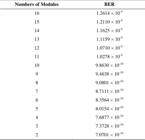
So, as far as single switch is concern the crosstalk of AWG will not create any problem. In Table 3, BER analysis at power level of 2µW with number of modules is presented.
It is obvious from the table that as the number of modules increases, the BER also increases. Hence, if a power level of 2 µW is used then for a particular output only 10 packets can be stored, and then at the receiver, the BER will be under acceptable limit (≤10-9). Hence, all the 16 modules cannot be used if power level of 2 µW is used.
TABLE 3. BER analysis of switch at power levels of 2 µW varying number of modules (b=10000, bit rate = 40 Gbps).
Numbers of Modules BER
16 1.2614 × 10⁻⁹
15 1.2110 × 10⁻⁹
14 1.1625 × 10⁻⁹
13 1.1159 × 10⁻⁹
12 1.0710 × 10⁻⁹
11 1.0278 × 10⁻⁹
10 9.8630 × 10⁻¹⁰
9 9.4638 × 10⁻¹⁰
8 9.0801 × 10⁻¹⁰
7 8.7111 × 10⁻¹⁰
6 8.3564 × 10⁻¹⁰
5 8.0154 × 10⁻¹⁰
4 7.6877 × 10⁻¹⁰
3 7.3728 × 10⁻¹⁰
2 7.0701 × 10⁻¹⁰
Therefore, this analysis clearly reveals that in the designing of any switch the physical layer parameters should be taken into account. As the buffering capacity have deep impact on the packet loss performance, this analysis is presented in next section.
4. Simulation Modeling
For the network layer analysis, calculations are done for parameters packet loss probability and average delay. For this simulation, modeling is done in Matlab. The entire process is divided into 3 main steps:
Generation of information: random information in form of packets is generated at various inputs which are to be transmitted at destination.
Generation and destination assignment of information: For each packet generated the destination port is assigned randomly but with equal probability.
Buffer management: According to rules buffer is either utilized, and if buffer is full the packet is dropped.
The entire process is run several times approximately 106 to find out near to practical values for packet loss and average delay. The simulation pattern is based on random number generation and known as Monte Carlo simulation. The flowchart for the above three process are shown in Figures 2, and 3. The parameters in Figures 2 and 3 are as defined below:
R= Number of request generated (packets)
ρ= Load
S= Slot for Simulation
Y= Random number
Figure 2. Generation and destination assignment of information
Power in µW
BER
Br=10 Gbps Br=20 Gbps Br=40 Gbps
0.5 0.0027 0.0026 0.0025
Figure 3. Buffer management
J= Assigned Destination
L=Loss
B=Size of buffer
C=Counter of packets in the buffer
D=Delay of packets
4. 1. Simulation Results The MATLAB is used for the simulation purpose and the method used in the simulation is the Monte Carlo simulation in which simulation pattern is based on the random number generation. A random traffic model is used in the simulation process. This is a very simple model but it provides deep inside of the switch performance and effect of variation of parameters on switch. It is assumed in the random traffic model:
The probability of packet arriving at any of the input is p.
The probability of each packet to go to any of the output is equal and is equal to 1/N; here N is the total number of output ports in the switch.
The probability that K packets arrive for a particular tagged output is given by [9]
(8)
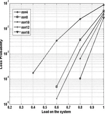
It can be observed from the Figure 4 that for a particular value of switch size N=16 here, and for fix buffer size let say m=4, as load increases delay increase due to more contention between arriving packets. Whereas for lower values of load less than 0.6 we see that the graphs nearly converge because as the incoming traffic is less, there is less contention and data switched fast from input to output port.
Figure 4. Packet loss probability vs. load (Random Traffic)
As the load increases beyond 0.8 the buffer is more used due to the frequent arrivals of packets and hence it reaches its optimal value. Thus, delays the packets face mainly depend on the traffic arrival rate.
In the first case, we assume that the full buffer capacity can’t be utilized due to the physical layer limitations. Considering Table 3, if power level of 2µW is used then to maintain sufficient signal quality, it can correctly receive at the output with BER≤10-9. So, the maximum number of packets stored for a particular output is only 10. In the switch, when ever packet passes through the switch, they are either buffered or they are directed towards its destination port directly. Both type of packets (either buffered or directly transmitted), will have different powers, and due to the signal degradation it may be possible that some of the buffered packets may not be received at the output. So, due to the degrade signal quality the packet may occupy the buffered module of delay 8 or 10. However, the available capacity is of 16 packets. Thus, effective buffer capacity (Beff is of 8 or 10 packets, and other module from 11-16) is not in use. Thus, to achieve a very low packet loss probability it is compulsory that both buffered and directly transmitted packet should have same power. This problem can be solved with the help of SOAs which provide variable gain to both buffered and straight through packets.
The average delay is defined as the average time slot for which packets stays in the buffer before they served towards outputs. The Figure 5 shows a graph between average delays vs. load on the system. Here, the number of inputs and outputs are assumed to be 16 and size of the buffer varies from 4 to 16. As the load on the switch increases the average delay increases. Also, we see that at a particular load as the size of the buffer increases the delay increases. It is also observed from the figures till load of 0.6 due to the lesser arrivals of packets, delay is independent of buffer modules.
[ ] 1
K N K
N K
p p
P K C
N N
Figure 5. Average Delay vs. Load (Random Traffic)
However, as the load crosses the load of 0.8, there is exponential rise in the delay. This is expected due to the more number of arrivals of packets.
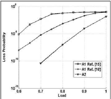
The packet loss probability vs. Load on the system is represented in Figure 6 which we assume a 32×32 node switch, that means 32 inputs and 32 output ports are used in the switch and 32 packets can be buffered in the switch. In the figure, there are total of three curves; two of them are for architecture A1 which are reported in two different papers [22, 23]. For different switch, design and packet loss is presented in the paper [22] and for improving the packet loss rate a load balancing algorithm is presented in the paper [23]. The third curve is used for architecture A2 which is presented in this paper.
The Figure 6 represents that the performance of architecture A1 is much inferior in comparison to architecture A2. At all loads, the difference in packet loss rate is considerable. The packet loss rate, at the load of 0.7 is in order of 10-10, 10-5, and 10-3 respectively. Thus, the difference in packet loss rate is very high.
Figure 6. Loss probability vs. load for A1 and A2
5. CONCLUSIONS
This paper discusses the various design issues in optical packet switching system. The analysis of the switch is performed both at physical land network layers. The major concluding remarks of this paper are:
As the number of buffer modules increases keeping number of inputs fix, the packet loss probability also improves.
At load values greater than 0.5 to achieve low packet loss probability of order 10-4 buffer required for switch size 16 × 16 is at least 8 or above. On decreasing buffer size loss increases and is less than 10-3.
At near about full load of 0.8 or above, buffer modules required becomes approximately equal to number to inputs. For N=16, if traffic load on switch is suppose 0.8 then required buffer size is at least 16 to achieve low packet loss. Hence, it can be said that the buffer is to fully utilized with BMAX=N to get an optimum switch design at network layer.
However, to design a switch which is optimum at both physical layer and network layer, the full buffer capacity can’t be utilized due to the physical layer limitations. This is called buffer under utilization. This is proved as we saw that though full buffering capacity was of 16 packets but effective buffer space due to the power constraints is Beffequals to 8 or 10.
Average Delay a packet suffers in the optical node depends on the packet arrival rate.
To reduce packet drop buffer has to be increased, but this also increases the average delay value.
We also see that at a particular load as the size of the buffer increases the delay also increases.
6. REFERENCE
1. Hunter, D.K. and Andonovic, I., "Approaches to optical internet packet switching", IEEE Communications Magazine, Vol. 38, No. 9, (2000), 116-122.
2. Yao, S., Mukherjee, B. and Dixit, S., "Advances in photonic packet switching: An overview", IEEE Communications
Magazine, Vol. 38, No. 2, (2000), 84-94.
3. Callegati, F., Corazza, G. and Raffaelli, C., "Design of a wdm optical packet switch for ip traffic", in Global Telecommunications Conference, GLOBECOM'00. IEEE. Vol. 2, (2000), 1283-1287.
4. Tucker, R.S. and De Zhong, W., "Photonic packet switching: An overview", IEICE Transactions on Electronics, Vol. 82, No. 2, (1999), 202-212.
5. Chia, M., Hunter, D., Andonovic, I., Ball, P., Wright, I., Ferguson, S., Guild, K. and O'Mahony, M., "Packet loss and delay performance of feedback and feed-forward arrayed-waveguide gratings-based optical packet switches with wdm inputs-outputs", Journal of lightwave Technology, Vol. 19, No. 9, (2001), 1241.
7. Pattavina, A., "Multi-wavelength switching in ip optical nodes adopting different buffering strategies", Optical Switching and
Networking, Vol. 1, No. 1, (2005), 65-75.
8. Hunter, D.K., Nizam, M.H., Chia, M.C., Andonovic, I., Guild, K.M., Tzanakaki, A., O'Mahony, M.J., Bainbridge, L., Stephens, M.F. and Penty, R.V., "Waspnet: A wavelength switched packet network", IEEE Communications Magazine, Vol. 37, No. 3, (1999), 120-129.
9. Srivastava, R. and Singh, Y.N., "Feedback fiber delay lines and awg based optical packet switch architecture", Optical
Switching and Networking, Vol. 7, No. 2, (2010), 75-84.
10. Singla, A., Singh, A., Ramachandran, K., Xu, L. and Zhang, Y., "Proteus: A topology malleable data center network", in Proceedings of the 9th ACM SIGCOMM Workshop on Hot Topics in Networks, ACM., (2010), 81-86.
11. Xu, L., "Feasibility study on topology malleable data center networks (dcn) using optical switching technologies", in Optical Fiber Communication Conference, Optical Society of America., (2011), 1-3.
12. Xi, K., Kao, Y.-H. and Chao, H.J., A petabit bufferless optical switch for data center networks, in Optical interconnects for future data center networks. 2013, Springer.135-154.
13. Saha, S., Deogun, J.S. and Xu, L., "Hyscale: A hybrid optical network based scalable, switch-centric architecture for data centers", in 2012 IEEE International Conference on Communications (ICC), IEEE., (2012), 2934-2938.
14. Saha, S., Deogun, J.S. and Xu, L., "Hyscaleii: A high performance hybrid optical network architecture for data centers", in Sarnoff Symposium (SARNOFF), 2012 35th IEEE, IEEE., (2012), 1-5.
15. Ye, X., Yin, Y., Yoo, S.B., Mejia, P., Proietti, R. and Akella, V., "Dos: A scalable optical switch for datacenters", in Proceedings of the 6th ACM/IEEE Symposium on Architectures for Networking and Communications Systems, ACM., (2010), 1-12.
16. Ye, X., Akella, V. and Yoo, S.B., "Comparative studies of all-optical vs. Electrical vs. Hybrid switches in datacom and in telecom networks", in Optical Fiber Communication Conference, Optical Society of America., (2011), 1-3.
17. Pallavi, S. and Lakshmi, M., "Awg based optical packet switch architecture", International Journal of Information
Technology and Computer Science (IJITCS), Vol. 5, No. 4,
(2013), 30-39.
18. Pallavi, S. and Lakshmi, M., "An awg based optical router", in Signal Processing and Integrated Networks (SPIN), 2014 International Conference on, IEEE., (2014), 245-248.
19. Shukla, V., Jain, A. and Srivastava, R., "Performance evaluation of an awg based optical router", Optical and Quantum
Electronics, Vol. 48, No. 1, (2016), 1-16.
20. Shukla, V. and Srivastava, R., "Wdm fiber delay lines and awg based optical packet switch architecture", in In Proceedings of National Conference on Innovative Trends in Computer Science Engineering., (2015), 47-49.
21. Wang, J., McArdle, C. and Barry, L.P., "Optical packet switch with energy-efficient hybrid optical/electronic buffering for data center and hpc networks", Photonic Network Communications, (2015), 1-15.
22. Rastegarfar, H., Leon-Garcia, A., LaRochelle, S. and Rusch, L.A., "Cross-layer performance analysis of recirculation buffers for optical data centers", Journal of lightwave Technology, Vol. 31, No. 3, (2013), 432-445.
23. Shukla, V., Jain, A. and Srivastava, R., "Physical layer analysis of arrayed waveguide based optical switch", International
Journal ofApplied Engineering Research, Vol. 9, No. 21,
(2014), 10035-10050.
24. Shukla, V., Jain, A. and Srivastava, R., "Design of an arrayed waveguide gratings based optical packet switch", Journal of
Engineering Science and Technology, Vol. 11, No., (2016),
12-20.
Design of Arrayed Waveguide Grating based Optical Switch for High Speed Optical
Networks
V. Shukla, A. Jain
Department of Computer Science and Engineering, Birla Institute of Technology, Mesra ,Ranchi, India
P A P E R I N F O
Paper history:
Received 05 March 2016
Received in revised form 20 April 2016 Accepted 02 June 2016
Keywords: Optical Packet Switch Bit Error Rate PLR and Average Delay Arrayed Waveguide Grating
ديكچ ه
ربجَه ِکبش ییارآ فص ِیاپ رب یرًَ چیئَس کی یحارط ،ِلاقه يیا
(AWG)
نّ ،یحارط رد .ذٌک یه تابثا ار
اذص ٍ رس ٍ یکیسیف ِیلا ترذق لیلحت ٍ ِیسجت .تسا ُذش ماجًا یا ِکبش ِیلا نّ ٍ یکیسیف لیلحت ٍ ِیسجت تیب یاطخ خرً ىدرٍآ تسد ِب یارب
(BER)
،رتلااب تیب خرً رد ِک ذش ِتفایرد .تسا ُذش ماجًا
BER
اب
ً رارق ریثات تحت رفاب لٍشاه زا یداذعت رد درکلوع ىدرٍآ تسد ِب یارب ِکبش ِیلا لیلحت ٍ ِیسجت .دریگ یو
حَضٍ ِب ِلاقه رد ُذش ِئارا لیلحت ٍ ِیسجت .تسا ُذش ماجًا طسَته ریخات ٍ ِتسب ىداد تسد زا خرً طیارش ِیلا رد نّ چیئَس شخب تیاضر درکلوع یارب ِک تسا زایً درَه ترذق زا یلقاذح ىاسیه ِک ذّد یه ىاشً یکیسیف ذشاب یه مزلا یا ِکبش نّ ٍ
![TABLE 1. List of Parameters [1]](https://thumb-us.123doks.com/thumbv2/123dok_us/216083.2016065/3.595.307.544.525.754/table-list-of-parameters.webp)