_____________________________________________________________________________________________________
Design of Common-Source/Drain Active Balun Using
90nm CMOS Technology
Frederick Ray I. Gomez
1,2*, Maria Theresa G. De Leon
1and John Richard E. Hizon
11University of the Philippines, Diliman, Quezon City, 1101, Philippines. 2
STMicroelectronics, Inc., Calamba City, Laguna, 4027, Philippines.
Authors’ contributions
This work was carried out in collaboration amongst the authors. All authors read, reviewed and approved the final manuscript.
Article Information
DOI: 10.9734/JERR/2019/v4i316906
Editor(s):
(1) Dr. Guang Yih Sheu, Associate Professor,Chang-Jung Christian University, Taiwan.
Reviewers:
(1) Tomas Ivaniga, University of Technology, Košice, Košice, Slovakia. (2)Dr. Michael Loong Peng Tan, Universiti Teknologi, Malaysia. (3)Etu Podder, Khulna University, Bangladesh. Complete Peer review History:http://www.sdiarticle3.com/review-history/48542
Received 13 January 2019 Accepted 07 April 2019 Published 19 April 2019
ABSTRACT
This research paper presents a design and study of a common-source/drain active balun circuit implemented in a standard 90-nm complementary metal-oxide semiconductor (CMOS) technology. The active balun design is intended for worldwide interoperability for microwave access (WiMAX) application, with operating frequency of 5.8GHz and supply voltage of 1V. Measurements are taken for parameters namely gain difference, phase difference, and noise figure. The common-source active balun design achieved a minimal gain difference of 0.016dB, phase difference of 180° ± 7.1°, and noise figure of 7.42-9.85dB, which are comparable to past active balun designs and researches. The design eventually achieved a low power consumption of 2.56mW.
Keywords: Common-source/drain active balun; 90nm CMOS; balun; gain; gain difference; phase difference; noise figure; WiMAX.
1. INTRODUCTION
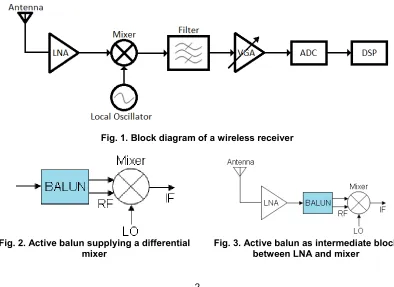
A considerable growth of interest in technologies that could deliver higher data rates over wider coverage led to the evolution of new wireless standards such as the IEEE 802.16-based WiMAX or the worldwide interoperability for microwave access. Like WiMAX, other communication systems namely Bluetooth, Wireless Fidelity (WiFi), and Long-Term Evolution (LTE) have the radio frequency (RF) receiver front-end that proves to be a critical part in the wireless system. A typical wireless receiver is represented in Fig. 1 diagram.
Some of RF front-end circuits are often designed as differential circuits. Fully-differential approach is usually preferred in RFIC design due to its advantages, particularly the high immunity to common-mode noises, rejection to parasitic couplings, and increased dynamic range [1-2]. In order to supply input signal to differential circuits, a building block capable of supplying balanced differential signals is needed without sacrificing the performance of the overall system in terms of gain, noise figure, and linearity. Active balun (balanced-unbalanced) is capable to perform the necessary tasks.
A balun circuit is a type of transformer that converts signals that are single-ended or unbalanced with respect to ground into signals
that are differential or balanced with respect to ground, and vice versa. Baluns can be classified as either active or passive baluns depending on the devices used. Active baluns, although unidirectional and more complex to implement, are preferred over their passive counterparts because they can produce gain, occupy less chip area and can operate at higher frequencies [2-3].
Active balun circuit can be used as the first block of the WiMAX receiver front-end to supply differential signal to a differential low-noise amplifier (LNA) [4]. It can also be used to supply differential signal to a mixer [5] in Fig. 2. Fig. 3 illustrates the active balun circuit as an intermediate block between the LNA and the mixer [6]. Note that the configuration depends on the gain, noise figure (NF), and linearity requirements of the system. Since LNA is the first block in the receiver front end, it is critically designed with high gain of at least 25dB and noise figure of less than 2dB. Based on past researches, active balun has relatively high noise figure and lower gain performance compared to LNA, hence cannot be considered as the first block in the receiver front-end. Finally, the challenge is to design an active balun as an intermediate block to allow the LNA’s output to connect with a differential mixer’s input, with performance conforming to the requirement for the WiMAX receiver front-end.
Fig. 1. Block diagram of a wireless receiver
Fig. 2. Active balun supplying a differential mixer
2. ACTIVE BALUN DESIGN
In this research paper, a common-source/drain active balun is designed and implemented in a standard 90nm complementary metal-oxide semiconductor (CMOS) technology. Process design kit (PDK) for standard 90nm CMOS process from CMP (Circuits Multi Projets) and STMicroelectronics was used for the design. The supply voltage (VDD) for the design is set to 1V.
The lengths (L) of all transistors are set to 100nm, which is the minimum allowed channel length for the technology used. Transistor widths (W) are carefully computed to ensure the operation of all the transistors at saturation. As mentioned earlier, the paper deals with the design of active baluns as intermediate block between LNA and mixer in the WiMAX receiver front-end. Table 1 summarizes the target specifications of the active balun design. These values are based from past active balun researches [5-8] and from the summary of parameters as per WiMAX standard [9].
Table 1. Target specifications for the common-source/drain active balun design
Parameters Value
Frequency 5.8GHz
Gain difference < 1dB Phase difference 180° ± 10° Noise figure < 10dB Power consumption < 10mW
Two important parameters of the active balun are the gain difference and phase difference. Gain difference is the difference of the gains from the two output nodes of the active balun while the phase difference is the difference between the phase of the non-inverting output node (RFout1) and the phase of inverting output node (RFout2) of the active balun. Another important parameter is the noise figure (NF), which is the measure of the amount signal-to-noise-ratio (SNR) degradation introduced by the circuit as seen in the output.
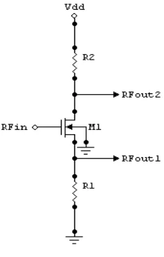
The common-source/drain active balun shown in Fig. 4 is composed of a single transistor M1. The input signal is fed into the gate of the transistor. Normal operation results in an inverted output signal at RFout2 and a non-inverted signal at RFout1. Ideally, these two outputs would have the same amplitude with a phase difference of 180º. Load resistors R1 and R2 determine the output voltages as well as the voltage gains of the two output signals with respect to the input signal.
Fig. 4. Common-source/drain active balun schematic
Common-source topology exhibits a relatively high input impedance while providing voltage gain and requiring a minimal voltage headroom. Common-drain topology or source-follower, on the other hand, is sometimes employed as level shifters or buffers, impacting the overall frequency response. It also exhibits high input impedance. With the two topologies merged to function as an active balun, common-drain will dominate the response on the overall voltage gain or attenuation because of the feedback effect of load resistor R1 with respect to the input.
Common-source/drain active balun is ideal for low voltage, low power WiMAX application due to low number of stacked devices. The active balun cannot actually produce gain in RFout1 due to its source-follower configuration. Since the two outputs should have balanced gain or attenuation, RFout2 should adjust and thus cannot produce gain. Hence, one important goal for this active balun design is to minimize the attenuation in outputs RFout1 and RFout2 and should be balanced with respect to the input RFin.
Drain current IDS of transistor M1 is also the total
supply current that is derived from the total power consumption of the active balun. With supply voltage VDD = 1V, IDS could be computed
in Eq. (1) in terms of the output DC or bias voltages V1 (or VRFout1) and V2 (or VRFout1) and the
output loads R1 and R2.
Assuming output loads R1 and R2 are equal to achieve a balanced response for V1 and V2 in
terms of output swing, Eq. (1) would become Eq. (2).
= 1 − (2)
From the expression in Eq. (1), increasing IDS
increases the output voltage V1, while output
voltage V2 decreases with IDS. To achieve the
minimum attenuation, V1 and V2 should take into
account the drain-to-source voltage VDS of
transistor M1. This will also maximize the output swing in RFout1 and RFout2. Ensuring that transistor M1 operates at saturation region, VDS
should be at least VDSAT or the overdrive voltage
VOV. With supply voltage VDD = 1V, overdrive
voltage VOV set to 200mV and with the two
outputs balanced, output voltage swings are computed as
= − ≥ → − ≥ 0.2 (3)
Substituting V1 expression in Eq. (2) into Eq. (3),
− (1 − ) ≥ 0.2 (4)
≥ 0.6 → 1 > ≥ 0.6 (5)
Output DC voltage V2 is computed to swing from
0.6V to 1V. Calculating for the output swing for V1,
− = , ≥ 0.2 → ≤ − 0.2 (6)
≤ 0.6 − 0.2 (7)
≤ 0.4 → 0.4 ≥ > 0 (8)
Output DC voltage swing for V1 is calculated to
range from 0V to 0.4V. As previously mentioned, V1 increases with IDS while V2 decreases with
IDS. To maximize the output swing in RFout1 and
RFout2, output DC voltages V1 and V2 should
have values median to their output range in Eq. (8) and Eq. (5), respectively. This would also safeguard transistor M1 to operate at saturation region with VDS of at least 200mV, while varying
IDS. The optimized values for output DC voltages
V1 and V2 are given as
= 0.2 (9)
= 0.8 (10)
With threshold voltage Vt set to 400mV, VOV set
to 200mV, V1 set to 0.2V, and VDS ≥ VDSAT = VOV,
input bias voltage could be determined in Eq. (11) to (12).
= − ≥ → ( − 0.2 ) −
0.4 = 0.2 (11)
= 0.8 (12)
With input DC voltage VIN set to 0.8V, it could
swing from maximum 1V to 0.6V. Maximum input voltage is set to align with the supply voltage VDD which is at 1V. Drain current IDS of
transistor M1 is also the total current that is derived from the total power consumption of the active balun. Using the square-law equation in Eq. (13), transconductance gm could be
computed in Eq. (14) to (15).
= ( − ) (1 + ) (13)
= = ( − )(1 + ) (14)
= ( − − 1)(1 + ) (15)
Substituting IDS from Eq. (13) into gm in Eq. (14),
an important design parameter could be determined, which is the gmoverId.
= =( )= = ∗ =( ) (16)
= =( ) (17) Proper DC input bias should be observed to realize good efficiency in terms of gmoverId. It can also be observed that the gmoverId is affected by the load resistance R1. For low power design, higher gmoverId is recommended [10]. As initially assumed, VOV is set 200mV for
minimum attenuation and/or maximum voltage swing in outputs RFout1 and RFout2 with respect to the input RFin. With this, gmoverId could be estimated in Eq. (18).
= = 10 (18)
It can be noted that to maintain the efficiency for low power consumption, lowering IDS would also
mean lowering gm. Transistor sizing depends on the target power consumption and likewise IDS,
thus, affecting gm. Transconductance gm is a key
parameter that determines the voltage gain of the active balun, which will be discussed in the succeeding section.
Resistors R1 and R2 could be determined given the setup for minimum attenuation and maximum voltage swing in the two outputs.
1 = = . 2 = = . (19)
Table 2. Common-source/drain active balun parameters expressions
Parameters Value
Input bias voltage 0.8V
Output DC voltage for maximum swing 0.2V (RFout1), 0.8V (RFout2)
Input impedance ∞
Output impedance, with resistor and capacitor loads R1 || 1/sC1 (RFout1), R2 || 1/sC2 (RFout2) Voltage gain, simplified (s = 0)
( ) (RFout1)
( ) (RFout2)
Output noise voltage [1 + ( + ) 1] (RFout1)
[1 + ( + ) 2] (RFout2)
Noise Figure 10 1 + ( )
∙ ∆ ∙ (RFout1)
10 1 + ( )
∙ ∆ ∙ (RFout2)
V2 set to the optimum value and VDD set to 1V,
decreasing the supply current (which is equal to IDS) would increase the value of R1 and R2.
Large resistor values contribute to more noise and parasitics. Since the active balun is targeted for low power consumption, tradeoff between drain current IDS and resistor values is inevitable.
Moreover, the design is optimized to meet the target performance specifications suitable for WIMAX receiver. The active balun was designed using Cadence Virtuoso software [11], a computer-aided design (CAD) tool and simulation software. The Composer Schematic program of the same software [11] is used for the transistor-level design, with the 90nm CMOS technology PDK. Moreover, Analog Artist tool of Cadence [11] was used for the simulation. Table 2 summarizes the common-source/drain active balun parameters.
3. RESULTS AND DISCUSSION
The common-source/drain active balun is characterized and designed to achieve the target specifications. The extraction of all device parameters for use in simulations is done using Synopsys Star-RCXT [12]. Simulations of the extracted view are done using Cadence Design Systems software. The active balun is designed to operate at 5.8GHz, which is a typical frequency for WiMAX applications. Measurements in the simulation plots are taken at 5.8GHz.
3.1 Gain and Gain Difference
There are many types of power gain defined for an amplifier. The most commonly specified and often the most useful is the transducer gain, GT.
It is defined as the ratio of the power delivered to the load to the power available from the source.
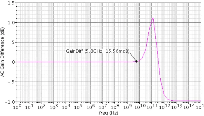
Gain difference or gain error is the difference of the gains from the two output nodes of the active balun, and is considered as one of the most important parameters of the active balun design. Ideally, the gain difference of an active balun should be zero in magnitude. The responses in Fig. 5 and Fig. 6 for the gain and gain difference, respectively, are determined using AC analysis. Ideal voltage source is used with input bias voltage VIN set to 0.8V. Drain-to-source voltage,
VDS,Q = V2 – V1, was measured at 528.6mV with
VGS – Vt = 71.6mV, confirming the transistor M1
operating at saturation. Fig. 5 shows the response using AC analysis.
Since the active balun has the configuration of common-drain, it is expected that the gains would fall below the target of at least 0dB. AC gains are at around -6dB. Take note that the three active baluns are designed with ideal voltage source at the input, thus with very high (if not infinite) input impedance, and the output is left with no termination. Since the resistor loads of the active balun are of the same value, gain difference was maintained very low at 0.015dB.
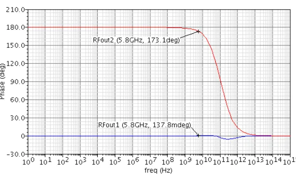
3.2 Phase and Phase Difference
Another important parameter of an active balun is the phase difference. Phase difference is the difference between the phase of the non- inverting output node and the phase of inverting output node of the active balun. Figs. 7 and 8 show the AC analysis phase and phase difference responses, with ideal input voltage source.
especially for the target phase difference with measurement at 172.9°.
3.3 Noise Figure
Noise performance is an important design consideration since it determines the susceptibility of the active balun to unwanted
signal or noise. One important design parameters is the noise figure (NF), which is a measure of the amount of signal-to-noise-ratio degradation introduced by the circuit as seen at the output. Fig. 9 shows the noise figure result using periodic steady-state + periodic noise (PSS+PNoise) analysis.
Fig. 5. AC analysis, gain plot
Noise figure of 7.422dB and 9.85dB for RFout1 and RFout2 with respect to RFin are generated using PSS+PNoise analysis with RF input power set to -20dBm. It is worth noting that the noise figure from PNoise analysis is slightly higher than the noise figure generated from SP analysis because at prf = -20dBm the active balun demonstrated very weak nonlinearity and noise as other high harmonics are convoluted.
3.4 Results Summary
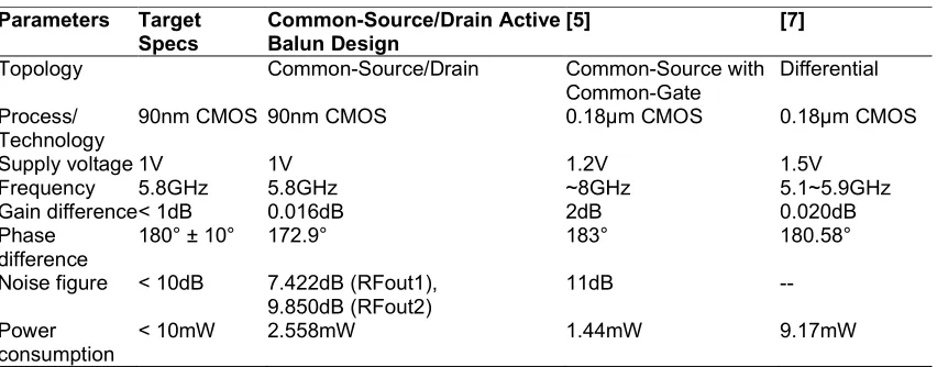
Table 3 summarizes the performance of the common-source/drain active balun design, and
comparison with past active balun designs and researches.
The common-source/drain active balun design achieved a gain difference better than 1dB and a phase difference of 180°±10° or better at frequency of 5.8GHz. The balun is affected with the input and output loading since the circuit is designed with ideal input voltage source and no termination ports included. Low power consumption of at most 2.56mW is achieved, comparable to other low power designs in the past researches.
Fig. 7. AC analysis, phase plot
Fig. 9. Noise figure plot
Table 3. Performance summary of common-source/drain active balun
Parameters Target Specs
Common-Source/Drain Active Balun Design
[5] [7]
Topology Common-Source/Drain Common-Source with
Common-Gate
Differential
Process/ Technology
90nm CMOS 90nm CMOS 0.18µm CMOS 0.18µm CMOS
Supply voltage 1V 1V 1.2V 1.5V
Frequency 5.8GHz 5.8GHz ~8GHz 5.1~5.9GHz
Gain difference < 1dB 0.016dB 2dB 0.020dB
Phase difference
180° ± 10° 172.9° 183° 180.58°
Noise figure < 10dB 7.422dB (RFout1), 9.850dB (RFout2)
11dB --
Power consumption
< 10mW 2.558mW 1.44mW 9.17mW
4. CONCLUSION AND RECOMMENDA-TIONS
A common-source/drain active balun is designed and implemented in a standard 90nm CMOS process, and carefully designed to satisfy the WiMAX receiver requirement at 5.8GHz. Simulation measurements are taken for parameters such as gain, phase, gain difference, phase difference, and noise figure.
The design achieved gain difference of less than 0.02dB and phase difference of 180° ± 7.1°. Noise figure performance is at around 7.42– 9.85dB, comparable to previous designs and researches. Low power consumption of at most
2.56mW is achieved, comparable to other low power designs.
Future work could include designing active balun with high gain. Although it will sacrifice the bandwidth, it can still be realized at lower frequencies for practical applications. One possible work would be to integrate the active balun functionality on the circuit design of a differential circuit like that of the double-balanced mixer or differential LNA.
ACKNOWLEDGMENTS
Technology (DOST), the Philippine Council for Advanced Science and Technology Research and Development under DOST (DOST-PCASTRD), and the Engineering Research and Development for Technology Consortium (DOST-ERDT) for the extensive support. The authors would also like to thank the Microelectronics and Microprocessors Laboratory team of the University of the Philippines for the technical support during the course of the study.
Author F.R. Gomez is greatly thankful to the ST Microelectronics Calamba Central
Engineering and Development Team and the Management Team for the utmost support.
COMPETING INTERESTS
Authors have declared that no competing interests exist.
REFERENCES
1. Crols J, Donnay S, Steyaert M, Gielen G. A high-level design and optimization tool for analog RF receiver front-ends. International Computer-Aided Design Conference. 1995;550-553.
2. Gomez FR, De Leon MT, Roque CR. Active balun circuits for WiMAX receiver front-end. TENCON 2010 – IEEE Region 10 Conference. 2010;1156-1161.
3. Azevedo F, Fortes F, Rosario MJ. A new on-chip CMOS active balun integrated with LNA. 14th IEEE International Conference on Electronics, Circuits and Systems. 2007;1213–1216.
4. Zhang HB, Cai M, Wu H, Chen HL. A 2.5GHz BiCMOS low noise and high-gain differential LNA for WLAN receiver. Asia Pacific Conference on Postgraduate Research in Microelectronics and Electronics. 2009;33-36.
5. Hsu TT, Kuo CN. Low voltage 2-mW 6~10.6-GHz ultra-wideband CMOS mixer with active balun. IEEE International Symposium on Circuits and Systems. 2006;5704-5707.
6. Shie CI, Hsieh CH, Chiang YC. UWB LNA and mixer with an active balun in 0.18 µm CMOS process. Asia Pacific Microwave Conference. 2009;1140-1143.
7. Do MA, Lim WM, Ma JG, Yeo KS. Design of a phase splitter for 3rd ISM band. IEEE Conference on Electron Devices and Solid-State Circuits. 2003;237-240.
8. Kawashima M, Nakagawa T, Araki K. A novel broadband active balun. 33rd European Microwave Conference. 2003;2: 495-498.
9. IEEE standard 802.16e-2005. Part 16: Air interface for fixed and mobile broadband wireless access systems, Amendment 2: Physical and medium access control layers for combined fixed and mobile operation in licensed bands, and Corrigendum 1. IEEE Computer Society and IEEE Microwave Theory and Techniques Society; 2006. 10. Yang HYD, Castaneda JA. Design and
analysis of on-chip symmetric parallel- plate coupled-line balun for silicon RF integrated circuits. IEEE Radio Frequency Integrated Circuits Symposium. 2003;527-530.
11. Cadence Design Systems, Inc. Custom IC / analog / RF design – circuit design. Available:https://www.cadence.com/conten
t/cadence- www/global/en_US/home/tools/custom-ic-analog-rf-design/circuit-design.html 12. Synopsys, Inc. StarRC – parasitic
extraction.
Available:https://www.synopsys.com/ implementation-and-signoff/signoff /starrc.html
© 2019 Gomez et al.; This is an Open Access article distributed under the terms of the Creative Commons Attribution License (http://creativecommons.org/licenses/by/4.0), which permits unrestricted use, distribution, and reproduction in any medium, provided the original work is properly cited.
Peer-review history: