Volume 3, Issue 5, May 2014
Page 94
Abstract
In this research, MgO thin films deposited on quartz glass and silicon substrate with different thicknesses 100 and 200 nm by a radio frequency (R.F.) magnetron sputtering process using magnesium oxide target under Ar gas pressure. The sputtering deposition was performed by using R.F. power of 130 Watt. The average surface roughness (Ra) measured with atomic force microscopy (AFM) was ranged between 8nm and 20nm. Spectral transmittance of MgO thin films were measured in the range of 200-1200 nm. Optical band gaps were calculated from Tauc' plots and
were found to be 5.5eV and 5.9eV for sample thickness of 100 nm and 200 nm respectively.
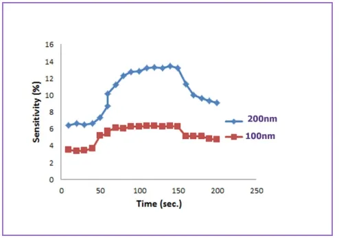
These films were tested in (NH3) gas at room temperature. The sensitivity after 100 sec from exposed to (NH3) gas were 6% and
13% for 100 and 200 nm film thickness respectively.
Keywords: MgO: Thin Film; Nanostructure; Optical; Gas Sensor and Sputtering RF.
1. INTRODUCTION
Magnesium oxide thin films are very important scientific and commercial material. They widely used as a protective layer for AC-plasma display panels because of their high durability and gas sensing systems[1].good protection characteristics against ion bombardment, high secondary electron emission coefficient and high transparency[2].MgO is a best candidate to be used as dielectric layer due to its excellent properties such as has high dielectric constant (~ 9.8), large band gap in the range of 7.3 eV -7.8 eV and has higher breakdown field (12 MV/cm) compared to commonly used dielectric layer which is silicon dioxide (SiO2) [2] . Due to its excellent dielectric properties,
MgO has been proposed to be used for capacitor applications because MgO can improve the storage capability of a capacitor. Other characteristics of MgO that comparable to SiO2are due to its chemical inertness, electrical insulation,
optical transparency, high temperature stability, high thermal conductivity and secondary-electron emission with a lattice constant of 4.21 Å [3]. Due to its excellent properties, MgO has been proposed to replace current dielectric material (SiO2) [4].Magnesium Oxide with rocksalt-structure has been extensively investigated due to its exceptional properties,
such as chemical inertness, high electrical resistivity, optical transparency, and low thermal conductivity [5–6].The most used techniques to obtain these films are organ metallic using thermal evaporation [7], flame spray paralysis [8], combustion aerosol synthesis [9], chemical vapor deposition [10], hydrothermal [11], and surfactant methods [12]
2. EXPERIMENTAL DETAILS
MgO thin films were prepared by RF magnetron sputtering system with a magnesium oxide target of 99.99% purity on quartz and (P+) silicon as substrates. Firstly, the target was pre-sputtered in an argon atmosphere in order to remove oxide layer. The argon gas was introduced into the chamber through a flow controller with fine adjustments the sputtering was performed under Ar (99.999%) atmosphere supplied as working gas through mass-flow controller. The sputtering chamber was evacuated down to 5 × 10⁻⁵ mbar by the turbo molecular pump. Microscope glass slides were used as the substrates for thin films. Prior to deposition, The quartz and (P+) silicon substrates was cleaned by chromic acid followed
by distilled water rinse.
The optical properties of the MgO films were, determined by The UV-VIS spectrum (Optima Sp – 300 Plus) was used to study the change of thickness on absorption, transmittance and band gap energy. For morphological investigations, AFM images were recorded using Nano scope IIIa scanning probe microscope controller in a tapping mode. In addition to the effect of thickness on sensitivity.
3.
Results and discussion:
3.1 Optical PropertiesThe optical characterization of thin films gives us something about the physical properties such as the absorption , transmittance and band gap energy and band structure, determined by UV-VIS spectrum(Optima Sp – 300 Plus ). Transmittance spectra recorded for MgO films as a function of wavelength range (200-1200 nm).It is observed that the
Influence of Thickness on Optical and Sensing
Properties of MgO Thin Films Deposited by RF
Magnetron Sputtering
Mahana M. Habeeb1, Muneer H. Jaddaa1, Abdul Hussein K.Elttayef2 and Hayder Mohammad Ajeel2
1
Volume 3, Issue 5, May 2014
Page 95
transmittance decreases with increase in thickness deposited with 100nm thickness shows higher transmittance compare to 200nm thickness as show in figure 1. This property of high transmittance makes it a good material for optical coatings. The optical band gaps of the films are calculated from the transmittance spectra. The absorption coefficient (α) iscalculated using the equation, [13]:
α= ln (1/T) / d …….. (1)
Where T is transmittance and d is film thickness. The absorption coefficient (α) and the incident photon energy
(hν) are related by the following equation [14]:
(αhν)2= A (hν-Eg) ……. (2)
The film it shows the representatives of optical absorbance which reveals that the absorbance of the film decreases gradually with increase in wavelength as shown in figure 2.
Fig.1. Transmittance Spectra of MgO Thin Films a. 100nm b. 200nm
Fig. 2. Absorbance Spectra of MgOThin Films a. 100nm b. 200nm
Volume 3, Issue 5, May 2014
Page 96
The typical plots of (αhν)2 versus hν for MgO thin films with 100nm thickness and 100nm thickness deposited on quartz
substrate is shown in figure (3). It is observed that increase in thickness of MgOlead to increase in optical band gap from 5.6eV to 5.9eV.
3.2 Morphology
The surface morphology of all the MgO films is offered by AFM images in tapping mode shown in Fig. 3. All the MgO films presentation a smooth surface with uniform grains.
In Fig. 3, the surface morphology discovers the nana-crystalline MgO grains, which rise to make intensive films significantly with the increased thickness. From the images, it was observed that the surfaces of the films exhibited a confirmed degree of coarseness and the film came rougher when the thickness increases.
Figure (4) Image AFM of Thickness (a) 100nm , (b) 200nm
3.3Gas sensing properties
The figure (5) shows the sensitivity to prepared MgO thin films on silicon p-type (n-p) by RF magnetron sputtering system with thickness 100nm and 200nm for the gas (NH3).The working gases were pumped in to the chamber and
recording the change in thin films resistance with time (per 10 seconds), MgO thin films suffer from the height of potential barrier in the reducer by using (NH3) gas closed to 6 ppm. The sensitivity is higher for sensors on the MgO with
200 nm thickness because increase in number of electrons lead to increased charge carries (electron - hole).
Figure (5) MgO thin Films Sensitivity NH3 a. 100nm b. 200nm
4. Conclusion
Volume 3, Issue 5, May 2014
Page 97
support the slow growth of crystallite sizes for the as-grown films and increasing thickness. The MgO films are highly transparent in the visible range and decreasing thickness causes slight increase in visible transmittance.It is observed that the allowed direct optical band gap of the films increases from 5.5 eV to 5.9eV with the increase of film thickness. The high sensitivity increasing thickness, the sensitivity was improved by increasing thickness.
References
[1] G. Ertl, H. Kno ¨zinger, J. Weitkamp (Eds.), Handbook of Heterogenous Catalysis, vol. 4, Wiley–VCH, Weinheim, 1997, p. 2111.
[2] Choi E-H, Oh H-J, Kim Y-G, J.-J. K, Lim J-Y, Kim J-G, Kim D-I, Cho G, Kang S-O, (1998) Jpn. J. Appl. Phys. 37 7015.
[3] I. -C. Ho, Y. Xu, and J. D. Mackenzie, "Electrical and Optical Properties of MgO Thin Film Prepared by Sol-Gel Technique," Journal of Sol-Gel Science and Te1. Renaud, G. Oxide surfaces and metal/oxide interfaces studied by grazing angle incidence X-ray
[4] E. Miranda, E. O'Connor, G. Hughes, P. Casey, K. Cherkaoui, S. Monaghan, R. Long, D. O'Connell, and P. K. Hurley, "Soft breakdown in MgO dielectric layers," in Reliability Physics Symposium, 2009 IEEE International, pp. 688-691, 2009
[5] Scattering. Surf. Sci. Rep. 1998, 32, 1–90. chnology, vol. 9, pp. 295-301, 1997.
[6] Nagashima, K.; Yanagida, T.; Tanaka, H.; Kawai,T. Epitaxial growth of MgO nanowires by pulsed laser deposition.J. Appl. Phys. 2007, 101, 124304:1–124304:4.
[7] Q. Yang, J. Sha, L. Wang, J. Wang, D. Yang, Mater. Sci. Eng., C 26 (2006) 1097 -1101. [8] Xie Yi, Wang Wenzhong, QianYitai, Yang Li, Chen Zhiwen, Surf. Coat.
Technol. 82 (1996) 291-293.
[1] G. Ertl, H. Kno ¨zinger, J. Weitkamp (Eds.), Handbook of Heterogenous Catalysis, vol. 4, Wiley–VCH, Weinheim, 1997, p. 2111.
[2] Choi E-H, Oh H-J, Kim Y-G, J.-J. K, Lim J-Y, Kim J-G, Kim D-I, Cho G, Kang S-O, (1998) Jpn. J. Appl. Phys. 37 7015.
[3] I. -C. Ho, Y. Xu, and J. D. Mackenzie, "Electrical and Optical Properties of MgO Thin Film Prepared by Sol-Gel Technique," Journal of Sol-Gel Science and Te1. Renaud, G. Oxide surfaces and metal/oxide interfaces studied by grazing angle incidence X-ray
[4] E. Miranda, E. O'Connor, G. Hughes, P. Casey, K. Cherkaoui, S. Monaghan, R. Long, D. O'Connell, and P. K. Hurley, "Soft breakdown in MgO dielectric layers," in Reliability Physics Symposium, 2009 IEEE International, pp. 688-691, 2009
[5] scattering. Surf. Sci. Rep. 1998, 32, 1–90. chnology, vol. 9, pp. 295-301, 1997.
[6] 4. Nagashima, K.; Yanagida, T.; Tanaka, H.; Kawai,T. Epitaxial growth of MgO nanowires by pulsed laser deposition.J. Appl. Phys., 101, 124304:1–124304:4,2007.
[7] Q. Yang, J. Sha, L. Wang, J. Wang, D. Yang, Mater. Sci. Eng., C 26 ,pp 1097 -1101,2006. [8] Xie Yi, Wang Wenzhong, QianYitai, Yang Li, Chen Zhiwen, Surf. Coat.
Technol. 82 ,pp 291-293,1996.
[9] J.J. Helble, J. Aerosol Sci. 29 ,pp 721-736,1998.
[10]Y. Li, Y. Bando, T. Sato, Chem. Phys. Lett. 359 ,pp 141-1452002.
[11]L. Kumari, W.Z. Li, C.H. Vannoy, R.M. Leblanc, D.Z. Wang, Ceram. Int. 35, pp 3355– 3364,2009. [12]P. Ouraipryvan, T. Sreethawong, S. Chavadej, Mater. Lett. 63 , 1862-1865,2009.
[13]W.Miao, X.Li, Q.Zhang, L.Huang, L.Zhang and X.Yan, “Transparent conducting In2O3 dopedMo thin films prepared by reactive direct current magnetron sputtering at room temperature”.Thin Sold Films, 500, pp 70,2006. [14]V.R.Shinde, T.P.Gujar, C.D.Lokhande, R.S.Mane and S.H.Han, “ Mn doped and undopedZnO films: A
comparative structural, optical and electrical properties study” Mater.Chem.Phys., 96, pp 326,2006.
Author
Mahana M. Habeeb, M.SC student in physics department, college of science, Wasit University. His research interest includes the preparation of nano films and applications.
Muneer H.Jaduaa, He is Assistant Proff. ,at physics dept., college of science, Wasit university. He is leading research group in the field of solid state and material Science.