RESEARCH
A fast image simulation algorithm
for scanning transmission electron microscopy
Colin Ophus
*Abstract
Image simulation for scanning transmission electron microscopy at atomic resolution for samples with realistic dimensions can require very large computation times using existing simulation algorithms. We present a new algo-rithm named PRISM that combines features of the two most commonly used algoalgo-rithms, namely the Bloch wave
and multislice methods. PRISM uses a Fourier interpolation factor f that has typical values of 4–20 for atomic
resolu-tion simularesolu-tions. We show that in many cases PRISM can provide a speedup that scales with f4 compared to
multi-slice simulations, with a negligible loss of accuracy. We demonstrate the usefulness of this method with large-scale scanning transmission electron microscopy image simulations of a crystalline nanoparticle on an amorphous carbon substrate.
Keywords: Scanning transmission electron microscopy, Electron scattering, Image simulation
© The Author(s) 2017. This article is distributed under the terms of the Creative Commons Attribution 4.0 International License (http://creativecommons.org/licenses/by/4.0/), which permits unrestricted use, distribution, and reproduction in any medium, provided you give appropriate credit to the original author(s) and the source, provide a link to the Creative Commons license, and indicate if changes were made.
Background
Transmission electron microscopy (TEM) is one of the most versatile and powerful experimental tools for imag-ing and diffraction of micrometer to sub-nanometer structures. The recent widespread adoption of hardware aberration correction has, in particular, enabled routine atomic resolution imaging of structures [1–3]. A more recent technical advance for TEM experiments is the use of direct electron detectors. These cameras have a much higher quantum efficiency than standard charge-coupled devices with a scintillator, and can also operate at much higher speeds [4–7]. Direct electron detectors have already created dramatic improvements in plane wave TEM imaging experiments, especially single-par-ticle biological cryo-EM studies [8–10]. These detec-tors have also enabled many new kinds of experiments for scanning transmission electron microscopy (STEM), where the electron probe is converged to very small dimensions and scanned across the surface of a sample, because the camera speed is high enough to record a full image of the diffracted probe at each probe position [11]. Examples include nanobeam electron diffraction strain
measurements [12, 13], orientation mapping of semi-crystalline polymers [14], and phase contrast imaging modes such as differential phase contrast [7, 15], phase plate interferometry [16], and ptychography [17]. Each of these experiments can benefit by accompanying them with STEM simulations to aid in interpretation or valida-tion of the results.
However, while the experimental capabilities of TEM and STEM have expanded, simulation methods have remained largely unchanged for some time. The two pri-mary methods currently used for atomic resolution sim-ulations are Bloch wave calcsim-ulations and the multislice method [18–20]. In the Bloch wave method, the electron wavefunction is defined using a basis set that satisfies the Schrödinger equation inside the sample. For a per-fect crystal, Bloch waves are stationary solutions with the same periodicity and symmetry as the crystalline lat-tice. After calculating the eigenvectors and eigenvalues of this basis set, the wavefunction at the entrance surface of the sample can be matched to the known electron probe coefficients, and then the resulting electron wavefunction can be computed everywhere (including the exit surface of the sample) [21, 22]. This scattering calculation can be written compactly in a scattering matrix (often called the
S-matrix) formalism [20]. Bloch wave calculations are almost never used for imaging or diffraction simulations
Open Access
*Correspondence: [email protected]
of large samples (beyond the several ‘unit cell’ scales for crystalline materials) for two reasons; the first is that eigendecomposition of a non-sparse Bloch wave matrix large enough to accurately simulate image sizes ≥10002
pixels would take an impractically long time to com-pute. The second is that the storage requirements of this scale of S-matrix are greater than a terabyte, and using it would require trillions of multiplication operations [20].
A more efficient formulation for large electron scatter-ing simulations is the multislice algorithm [23]. In this method, the atoms of the simulated sample are divided up into infinitely thin slices along the beam direction. The resulting electron scattering is calculated by alternating between a transmission operator through each slice, fol-lowed by Fresnel propagation of the electron wave to the next slice. These operations can be performed efficiently in realspace and reciprocal space, respectively, and so an efficient implementation of this method requires a for-ward and inverse Fourier transform at each step [20]. The multislice algorithm is very efficient for plane wave, conventional TEM image, or diffraction simulations. It is much less efficient for STEM simulations consisting of thousands or millions of probe positions. This is because while the atomic scattering potential can be reused for all probe positions, the transmission and propagation steps must be repeated for each additional probe position. The scattering potential calculations can be performed very efficiently using lookup tables [16, 24] or a point scatter-ing method [25], but the slow part of the calculation is usually repeated for all probe positions [20]. Many STEM studies such as high precision 2D measurements [26–28], 3D atomic electron tomography [29, 30], and others [31] make use of image simulations of many thousands of STEM probe positions. This requires long computation times, even with modern implementations of the mul-tislice method [25, 32–37]. It is therefore desirable to develop an electron scattering simulation algorithm that shares the calculation burden between STEM probe posi-tions in a more efficient manner than multislice simula-tion. Chen et al. [38] have proposed one such method, but it has not found widespread application. For a detailed discussion of the relationship between the Bloch wave and multislice simulation methods, we refer readers to the derivations of Allen, Findlay et al. [18, 19].
In this manuscript, we derive a more efficient algo-rithm for STEM simulations by combining aspects of the multislice and Bloch wave methods. We use the mul-tislice method to directly calculate a subset of the rows of the S-matrix (corresponding to plane waves of various orientations), which is then used in a similar manner as Bloch wave calculations [38] to relate the output wave-function to a given input. The key insight is that because highly converged STEM probes decay to zero quickly
with distance from the probe center position, they can be cropped out of the full S-matrix in a highly accurate Fourier interpolation scheme. The algorithm presented here is referred to as the plane wave reciprocal space interpolated scattering matrix (PRISM) algorithm. We also compare the accuracy and computation time of the PRISM and multislice algorithms, and suggest some use-ful extensions of the PRISM method.
Theory and methods
The multislice and Bloch wave methods
For previously published TEM simulation methods, we will briefly outline the required steps here. We refer read-ers to Kirkland for more information on these methods [20]. We will also only describe the scattering of the elec-tron beam while passing through a sample; probe-forming optics and the microscope transfer function mathemat-ics are described in many other works. All elastic scat-tering TEM simulations aim to describe how an electron wavefunction ψ (r) evolves over the 3D coordinates
�
r=(x,y,z) . The evolution of the slow-moving portion of the wavefunction along the optical axis z can be described by the Schrödinger equation for fast electrons [20]
where λ is the relativistic electron wavelength, ∇xy2 is the
2D Laplacian operator, σ is the relativistic beam sample interaction constant, and V(r) is the electrostatic poten-tial of the sample.
The Bloch wave method uses a basis set that satisfies Eq. 1 everywhere inside the sample boundary, which is assumed to be periodic in all directions. This basis set is calculated by calculating the eigendecomposition of a set of linear equations that approximate Eq.1 up to some maximum scattering vector |qmax|. Then, for each required initial condition such as different STEM probe positions on the sample surface, we compute the weight-ing coefficients for each element of the Bloch wave basis set. Finally, the exit wave after interaction of the sample is calculated by multiplying these coefficients by the basis set. This procedure can be written in terms of a scattering matrix S as [20]
where ψ0(r) and ψf(r) are the incident and exit
wave-functions, respectively. The Bloch wave method can be extremely efficient for very small simulations, where the field of view is on the scale of crystalline unit cells. High symmetry is also an asset for Bloch wave simulations, as we can limit the beam of plane waves (beams) included in the basis set to a small number. However, for a large STEM simulation consisting of thousands or even millions of
(1)
∂ψ (�r) ∂z =
i 4π∇xy
2ψ (�r)+iσV(�r)ψ (�r),
(2)
atoms in the simulation, the S-matrix may contain billions or more entries, which requires an impractical amount of time to calculate the eigendecomposition. And, actually using Eq. 2 many times for various electron probes could take a very long time. Thus, Bloch wave methods are typi-cally only used for very small size STEM simulations.
The most commonly employed method for large STEM simulations is the multislice algorithm. The mul-tislice method alternates between solving the two terms on the right-hand side of Eq. 1, for thin slices of thick-ness t taken from the sample. The left term is interpreted as a Fresnel propagation operator, which can be effi-ciently applied in Fourier space as [20]
where �(q)=F{ψ (r)} is the Fourier transform of ψ (r) ,
�
q=(qx,qy) is the 2D coordinate vector for Fourier space,
and the subscript p refers to the slice index. The second operator of Eq. 1 can be efficiently applied in real space as
where Vp2D(r) is the 2D electrostatic potential of all atoms inside slice p, integrated over the slice along the beam direction from the 3D potential. In practice, the atomic potentials are integrated into 2D potentials before the simulation, and then added directly to the slice poten-tial, or applied using convolution [25]. These two steps describe how the electron wavefunction evolves slice-by-slice until it has interacted with the entire sample, applied sequentially as
where F−1{} is the inverse Fourier transform. The
mul-tislice method is simple to implement and very accurate, but is not very efficient for large-scale STEM simulation. The reason is that although the atomic potentials can be reused for different probe positions, the remainder of the calculation (using Eq. 5 to propagate each probe though the sample) must be run independently. While this problem is amenable to parallelization, none of the calculations are shared between different probe posi-tions, or different probe parameters such as defocus, convergence angle, or probe tilt. In the next section, we will show how a STEM simulation can be reformulated into an S-matrix approach, where the computational load of applying Eq. 5 can be shared between different probe configurations.
The PRISM algorithm for STEM simulations
The first step of the method proposed here is to sepa-rate all atomic coordinates of the simulation cell (which
(3)
�p+1(q�)=�p(q�)exp(−iπ|�q|2t)
(4)
ψp+1(�r)=ψp(�r)exp
iσVp2D(�r),
(5)
ψp+1(�r)=F−1
Fψp(�r)eiσVp2D(�r)
e−iπ|�q|2t,
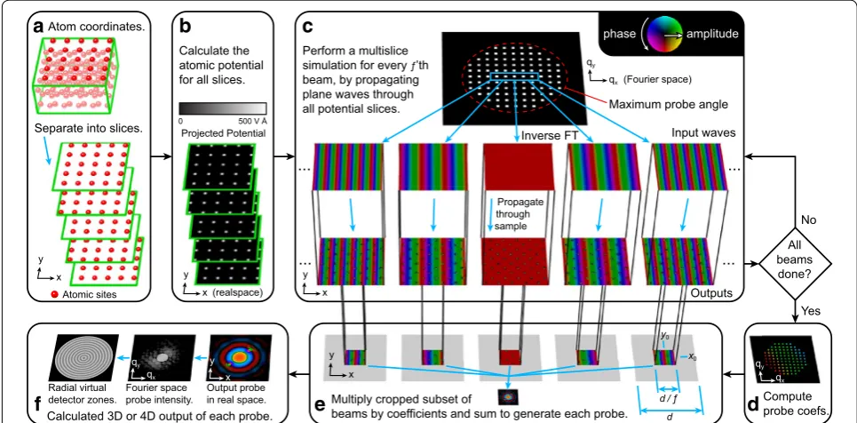
is assumed to be orthorhombic here) into slices, as shown in Fig. 1a. These slices can have unequal thickness to better match the atomic coordinates, but should not have thicknesses larger than the average atomic spacing as this could cause errors [20]. The second step is to cal-culate the 2D projected potentials V(r) for all slices, as shown in Fig. 1b.
Next, we choose an interpolation factor f. In practice, a different factor can be used in x and y, but for simplic-ity we will describe the simulation method for a square [in the (x, y) plane] simulation cell of size d. This factor
f should be chosen to be large enough so that a square area with a side length of the simulation cell size divided by f can encompass all possible STEM probes after they pass through the cell. This can be estimated by numeri-cally simulating a few probes using the conventional multislice method or the method described here. We then also choose a maximum incident probe semi-angle αmax. Note that the simulation will include larger scatter-ing angles than this value, and that this value should be equal to the largest desired probe semi-angle plus f times the Fourier space pixel size q. We then determine a set of plane wave initial conditions to simulate using the multislice method, as shown in Fig. 1c. This set of plane waves corresponds to the incident electron probe
where √m2+n2f�q≤αmax, δ(q) is the delta func-tion, and (m, n) are integers representing the plane wave index. Thus, we compute only a subset of all pos-sible periodic plane waves for the simulation cell size, reducing the number of waves calculated by a factor of
f2. These plane waves are stored in realspace in a large
array that we will refer to as the compact S-matrix, with the output plane waves defined as Sm,n(r). These output wave dimensions can be reduced by a factor of 4, if the multislice simulation uses an antialiasing aper-ture positioned at half of the maximum scattering angle [20].
Next, we calculate each converged electron probe at position �r0=(x0,y0) by first computing the required coefficients αm,n(r0) for each plane wave Sm,n(r), and then multiplying these coefficients by the associated plane wave basis and summing over a square subre-gion with side length d centered around the probe. This is shown schematically in Fig. 1d. The subregion is bounded by
(6)
�m,n(q)� =δ(qx−mf�q, qy−nf�q),
(7)
x0− d
2f ≤x<x0+ d 2f
y0− d
giving a cutout region having an area of d2/f2, which
should be periodically wrapped around the simulation cell boundaries. The wave coefficients are defined as
where A(q) is the probe aperture function defined as
The probe can also contain coherent wave aberrations such as defocus C1 or 3rd order spherical aberration C3
described by the phase shift function [20]
Finally, the terms htan(θx) and htan(θy) shift the probe back to the center of a cutout region for a given simula-tion cell of height h and probe tilt angles θx and θy. As shown in Fig. 1e, once the probe coefficients αm,n(r0) have been computed, the complex probe in realspace
ψ (r,r0) can be computed using the summation
(8) αm,n(�r0)=A(q�)exp[−iχ (q�)]exp−2iπq�
· [x0−htan(θx),y0−htan(θy)],
A(q�)= 1 where |�q| ≤qprobe 0 elsewhere.
(9)
χ (q�)=π|�q|2C1+ π 2
3|�q|4C 3+ · · ·
(10)
ψ (�r,�r0)=
m,n
Sm,n(�r) αm,n(�r0),
in the cut out region defined by Eq. 7. Note that this expression is simply an expanded form of Eq. 2. Equa-tion 10 can be evaluated more quickly if we skip the addition of all terms where αm,n(�r0)=0. After the probe is computed, we can either output the full probe diffraction pattern, or more commonly integrate a sub-set of the probe intensity after taking its Fourier trans-form, as shown in Fig. 1f. Once the output signals of all probes have been tabulated, the simulation is complete. Our method is very similar to that proposed by Chen et al. [38]; but, where they include tilts of the various beams in the propagation operator, we have included it in the initial conditions of each beam, which negates the need for an offset term to relate the relative phases of the beams.
Simulation and analysis implementation
All simulations and analysis in this study were performed using custom Matlab code. The multislice methods and the atomic potentials employed were taken from Kirk-land [20]. Thermal scattering effects were implemented using the frozen phonon approximation, which involves repeating the calculation with different phonon configu-rations (approximated with random atomic displace-ments) and summing the results incoherently.
Perform a multislice simulation for every ƒ’th beam, by propagating plane waves through all potential slices. Calculate the
atomic potential for all slices.
Projected Potential 0 500 V Å
Atom coordinates.
Separate into slices.
Maximum probe angle
Input waves
Outputs
All beams done?
Compute probe coefs.
Yes No
Multiply cropped subset of
beams by coefficients and sum to generate each probe. Calculated 3D or 4D output of each probe.
Output probe in real space. Fourier space
probe intensity. Radial virtual
detector zones.
...
...
...
... Propagate
through sample
d / ƒ x0 y0
d
a
f
e
d
b
c
phase amplitudeAtomic sites x (realspace) y
x y x
y
x y
x y
qx(Fourier space) qy
qx qy qx
qy
Inverse FT
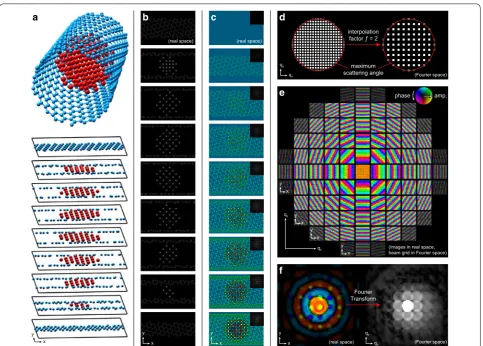
An implementation of the PRISM algorithm for a sam-ple consisting of a nanoparticle contained within a car-bon nanotube is shown in Fig. 2a–f. Each of the panels in this figure corresponds to the same step as those given in Fig. 1a–f. In Fig. 2c, e and f, the wave phase is shown as the color hue, while the wave amplitude is shown by the brightness of each pixel. All simulations were performed using an 80 kV accelerating voltage, a slice thickness of 0.2 nm, a pixel size of 0.01 nm, and we used no spherical aberration in the electron probes.
Calculation time for PRISM simulations
We will now approximate the computation time of the PRISM algorithm, relative to traditional multislice simu-lations. We will neglect the computation time of the sam-ple projected potential slices, as this calculation time is equal for both methods. We will also not consider ther-mal scattering, since it will require an increase in calcu-lation time by an equal multiplier for both methods. For
simplicity, we will assume a square simulation cell with side length N where N is a power of two. Each slice will require the transmission and propagation operations given in Eq. 5, which requires 6Nlog2(N) complex opera-tions for the forward and inverse Fourier transforms and 2N2 operations to multiply the sample potential and the
Fresnel propagation functions. If the entire STEM simu-lation consists of P unique probe positions and H slices through the sample, the total calculation time Tmulti
required is
if the simulation cell is large, i.e., N ≫1. The PRISM method requires two parts to compute the scattering of all STEM probes. The first half of the algorithm requires
B/F2 multislice simulations, where B is the number of
beams included in the full-resolution simulation, which
(11)
Tmulti=HP
6Nlog2(N)+2N2
≈2HPN2,
a b c d
interpolation factor ƒ = 2
Fourier Transform maximum scattering angle
e
f
x y
x y
x y x y
x y
x y qx
qy
qx qy qx
qy
x y
x y
phase amp. (real space) (real space)
(Fourier space)
(real space) (Fourier space) (images in real space, beam grid in Fourier space)
Fig. 2 Example implementation of the PRISM algorithm. a The sample’s atomic coordinates are divided up into slices. b The projected potential of each slide is computed. c Each required plane wave is calculated by using the multislice algorithm to propagate the wave through the sample.
will be reduced by the interpolation factor squared. The second half is the multiplication of the compact scat-tering matrix S for all beams (multislice plane waves computed in the previous step), which is required for P
total probes, as in Eq. 10. This multiplication step is only required for the reduced number of beams B/F2, and the
cut out region defined by Eq. 7 will reduce the number of multiplication operations to N2/4f2 (note the extra factor
of 1/4 is due to storing only the part of S inside the anti-aliasing aperture). Therefore, the total calculation time
TPRISM required for PRISM is
Note that for a STEM probe, the probe amplitude coef-ficients beyond the probe semi-angle are zero and so the number of beams B used in practice is often much lower than the number of possible beams. The speedup offered by the PRISM algorithm is therefore approximately equal to the ratio of Eqs. 11 and 12 given by
If the rate-limiting computation step for the PRISM algorithm is multiplying out the compact S-matrix, the speedup ratio does not depend on the number of probe positions P and the speedup will vary with f4. In
the multislice and PRISM simulations given in the first results section below, the values of the terms of Eq. 13
were H = 40, B = 104, and P = 105. Plugging these
num-bers into Eq. 13 gives a speedup factor TMulti/TPRISM of
approximately 0.5, 8, 110, and 1100 for f = 2, 4, 8, and 16, respectively.
Results and discussion
Comparison of accuracy between multislice and PRISM
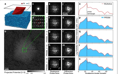
In general, PRISM will always be less accurate than cor-responding multislice calculations, unless the PRISM speedup allows for finer pixel sampling, inclusion of higher scattering angles, or a similar improvement. How-ever, the increased error is negligibly small in many cases, and will depend heavily on the microscope and sample parameters of a given simulation. To demonstrate this, we have compared the accuracy of a STEM probe cal-culation for a typical experimental geometry: a Pt nan-oparticle (NP) approximately 7 nm diameter tilted 30° from the primary axis. The NP rests upon an amorphous carbon substrate with a thickness of 5 nm, as shown in Fig. 3a. The NP has a multiply twinned decahedral struc-ture, with screw and edge dislocations present in two of
(12)
TPRISM=
HB f2
6Nlog2(N)+2N2
+ PBN
2
4f4
≈BN2
2H f2 +
P 4f4
.
(13)
TMulti
TPRISM =
8HPf4 B(8Hf2+P).
the grains. The NP atomic coordinates were taken from [39], and the amorphous carbon structure was adapted from [40].
The sample was divided up into slices 0.2 nm thick, and the projected potential was computed for all slices. The sum of these potentials is shown in Fig. 3b, with an enlarged inset shown in Fig. 3d. The initial STEM probe generated from a 25 mrads semi-angle aperture at 80 kV is shown in Fig. 3c, with the probe center position shown in Fig. 3d. We then calculated the probe wavefunction after passing through the sample using the multislice method (Fig. 3e) and the PRISM algorithm with interpo-lation factors of f = 2, 4, 8, and 16 (Fig. 3f–i). The cor-responding probe amplitudes in Fourier space are shown in Fig. 3j–n, respectively, and the logarithm of the radially integrated intensities is plotted in Fig. 3o–s, respectively. In the real space images, the channeling effect along aligned atomic columns is visible in all simulations [41].
We see that the PRISM method correctly reproduces most of the fine structure in the real space probe images. In Fig. 3i, we see that when f =16, the tails of the probe have been cut off by the edge of the cropping window, leading to small artifacts at the boundary (shown with white arrows). However, Fig. 3n, s shows that this simula-tion can still qualitatively reproduce the diffracted probe signal with good accuracy.
Two small differences between the PRISM and mul-tislice simulations are visible. The first is the “blurring” effect caused by the Fourier interpolation, an effect which increases as f increases in Fig. 3k–n. This is reflected in the radially integrated intensities, as a small mixing between adjacent detector angle bins. Secondly, there is a small decrease in intensity at the highest scattering angles. This decrease is very small, visible only because of the logarithmic intensity scale. The source is probably the interpolation step of PRISM, which will reduce the image sharpness slightly, manifesting at the highest spa-tial frequencies/scattering angles. We therefore conclude that PRISM is accurate enough to replace the traditional multislice method for STEM simulations in most cases. The primary exceptions are when the probe is very large (highly defocused or delocalized) or when fine details must be recovered from diffraction pattern, such as higher order Laue zone line measurements [42].
is slightly increased to prevent sampling artifacts at the edge of the 20 mrad semi-angle electron probe.
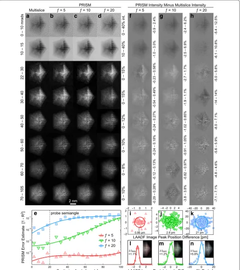
Figure 4a, b demonstrates that for relatively low inter-polation factors, PRISM is essentially identical to Mul-tislice simulations. PRISM can accurately capture the coherent diffraction image contrast present at lower scat-tering angles. Additionally, it can reproduce the clean mass-thickness contrast signal present at high scatter-ing angles. As the interpolation factor is increased, sub-tle differences from the multislice image simulations do emerge, in Fig 4c–d. However, the image contrast is still qualitatively very similar to the multislice images. The primary advantage of PRISM is the reduced calculation time; the PRISM simulations with interpolation factors of f =5, 10, and 20 gave speed up factors of approxi-mately 40, 280, and 2100, respectively, compared to the multislice simulation. The f =20 simulation shown in
Fig. 4d requires only a few minutes of calculation time on a modern desktop computer, using Matlab code that has not been highly optimized or compiled.
Figure 4e shows an error estimate for the three PRISM simulations in Fig. 4b–d. The error was estimated as
1−R2, where R2 is the correlation coefficient between the
multislice and PRISM simulation pixel intensities. The f =5 PRISM simulation error is approximately 0.005% for all scattering angles, indicating that this simulation is essentially error-free. When the interpolation factor is increased to f =10, the difference from a multislice sim-ulation increases to an error of 0.05% for low scattering angles and ≈1% error for intermediate scattering angles,
and finally ≈10% for high scattering angles. Doubling
the interpolation factor again to f =20 gives 1% error
at small scattering angles and 10% error for medium and high scattering angles. This larger error is caused by the region cropped around the STEM probe being small enough to crop out a significant portion of the probe intensity and cause boundary errors, as shown in Fig. 3i. We conclude that when using a low enough interpolation factor f, the PRISM method can simulate STEM intensi-ties at all scattering angles with negligibly low error. The Pt
0
102 103 104 20Scattering Angle [mrads]40
Log Radially Integrated Intensity [arb. units.
]
PRISM, ƒ =
4P
RISM, ƒ =
2
PRISM,
ƒ = 16
PRISM,
ƒ =
8
Multislice
Multislice
probe semiangle
PRISM
Realspace
Probe Amp. Probe Amp.Diffraction Projected Potential [V·Å]
1 nm
60 80
a
b
C e
f d
g
h
i
j
k
l
m
n
o
p
q
r
s c
2 Å 20 nm-1
Fig. 3 Comparison of Multislice and PRISM simulations of a single converged electron probe. a Three-dimensional view of the atomic structure consisting of a defected Pt decahedral nanoparticle, resting up an amorphous carbon support. Entrance and exit planes shown in black. b Sum of projected potentials with inset around probe position shown in d, and initial probe amplitude at the same location shown in c. Realspace images of probe amplitude after passing through sample for e the multislice method, and f–i using various interpolation factors f for the PRISM method. Diffraction space images of probe amplitude after passing through sample for j the multislice method, and k–n using various interpolation factors f
Multislice
a
e
b
c
d
0 – 10 mrads
10 – 15
22 – 30
30 – 40
40 – 50
50 – 60
60 – 70
70
– 105
PRISM Error Estimate [1 -
R
2]
Scattering Angle [mrads] LAADF Image Peak Intensity Difference [% Probe]
LAADF Image Peak Position Difference [pm] 0.86 pm 2.8 pm
probe semiangle
0 – 40% int
.
10 – 40
%
0 – 15
%
0 – 15
%
0 – 12
%
0 – 10
%
0
– 8%
0 – 10%
-0.9 – 2.4%
-1.0 – 3.0%
-0.23 – 0.58
%
-0.54 – 0.49
%
-0.24 – 0.27
%
-0.24 – 0.18
%
-0.12
– 0.13
%
-0.29 – 0.28
%
-2.4
–
6.2%
-2.5
– 6.9%
-2.7 – 1.7%
-1.9 –
1.1%
-1.02 –
0.85
%
-0.91
– 1.05
%
-0.82
–
0.97
%
-3.8 – 3.8%
-5.4
– 12.5%
-6.1
– 10.8
%
-5.0
–
5.8%
-14 –
14
%
-8.0 –
7.1%
-5.6 – 5.9%
-4.8
– 4.6%
-7.1
– 7.1%
ƒ = 5 PRISMƒ = 10
2 nm
ƒ = 20
ƒ = 20 ƒ = 10 ƒ = 5
ƒ = 5
PRISM Intensity Minus Multislice Intensity
ƒ = 10 ƒ = 20
0 20 40 60 80 100
10−4 10−3 10−2 10−1
−2 0 2 −2 −1 0 1 2
−2 −1 0 1 2
−2 0 2 −4 −2 0 2 4
−4 −2 0 2 4
−20 0 20 −40 −20 0 20 40
−40 −20 0 20 40
21 pm
f
g
h
i
j
k
l
m
n
∆ IRMS
=1.1% ∆ IRMS=1.2% ∆ IRMS=5.8%
Fig. 4 STEM simulations of a Pt particle on amorphous carbon, using a 20 mrad STEM probe at 80 kV. a Multislice and b–d PRISM image simula-tions for interpolation factors of f =5, 10, and 20, respectively. Each row corresponds to a different annular virtual detector, with the inner and outer
scattering angles labeled on the left. The intensity of each row was kept constant, in units of total probe intensity with the range shown to the right.
e Error estimates as a function of scattering angle for the PRISM simulations in b–d. f–g Intensity differences between PRISM and multislice images, with plot ranges given to the right. i–k Peak positions differences and l–m peak intensity differences for 360 peaks fitted from LAADF images, between multislice simulations and PRISM simulations with f=5, 10, and 20, respectively. Mean position and RMS intensity differences, and the
best value for f can be determined by testing probes at different locations in the simulation cell with both PRISM and multislice, or by using a conservative, low value; for example, in this simulation f =5 leads to a cutout region with side length 2 nm, large enough to contain the entire STEM probe for any probe semi-angle large enough to generate atomic resolution contrast.
Figure 4f–h shows the difference in intensities between the PRISM image simulations in Fig. 4b–d, respectively, and the multislice image simulations in Fig. 4a. The intensity range for each panel is set individually to show good contrast for the features present. Figure 4f shows that when f is small, PRISM will slightly over-estimate the image intensity at scattering angles below the probe semi-angle, and slightly under-estimates the intensity at higher scattering angles. These intensity differences are probably caused by the different sampling of PRISM compared to multislice for both defining the initial electron probe, and creating the virtual detectors for the output signal. The errors for f =5 also appear to be primarily intensity errors, which will not strongly affect measurements such as peak position estimation. Fig. 4g and h shows larger intensity differences for f =10 and 20. These differences
depend on the amount of local scattering and the local tilts of atomic columns, which could introduce errors in peak position measurements.
To test the accuracy of using PRISM to estimate struc-tural information, we have used non-linear least squares peak fits using a 2D Gaussian function to measure 360 of the strongest peaks on the right-hand side of the deca-hedral particle as shown in Fig. 4. These peaks were measured from low-angle annular dark field (LAADF) images created with a virtual detector from 22.5 to 105 mrads. We have plotted the differences in measured peak positions between multislice and PRISM simula-tions in Fig. 4i–k, and the peak intensity differences in Fig. 4l–m. The mean 2D position errors for the PRISM simulations are 0.86, 2.8, and 21 pm for f =5, 10, and 20, respectively. These errors will decrease if more frozen phonon configurations are included due to the increas-ing smoothness of the peak functions in the simulated images. Additionally, the errors could be reduced by using a probe sampling finer than 0.25 Å. The intensity differences in the peaks are fairly small, ≈1% for both f =5 and 10. When f is increased to 20, the intensity errors increase rapidly, underlining the importance of choosing an f value low enough for the desired accuracy.
PRISM simulations with varying probe size
In the PRISM method, once the compact S-matrix is computed for a given set of atomic coordinates, it can be used for many different simulations. The primary change between electron probes is not only the probe center
position, but we can also vary coherent wave aberrations in the probe such as defocus or spherical aberration, change the probe size by modifying the probe semi-angle radius, and also include relative tilt between the probe and sample by moving the probe center away from �
q=(0, 0). These simulation parameter changes reflect only changes in the probe weighting coefficients αm,n(r0) , given in Eq. 10.
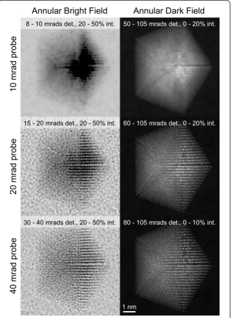
An example of using the same S-matrix to simulate STEM images with varying probe size and annular detec-tors is shown in Fig. 5, for an accelerating voltage of 80 kV and a probe spacing of 0.025 nm. Based on the previ-ous results shown in Fig. 4, we have chosen an interpola-tion factor of f =5 for these simulations. In Fig. 5, we have generated annular bright-field images by setting the detector inner and outer angles to ≈75 and 100% of the probe semi-angle, respectively. Annular dark field images were generated by setting the detector inner angle to 40 mrads outside of the probe semi-angle. These simula-tions show that for this sample, a 10 mrad probe does not generate atomic resolution contrast. However, a 20
Annular Bright Field
10 mrad probe
20 mrad probe
40 mrad prob
e
Annular Dark Field 8 - 10 mrads det., 20 - 50% int. 50 - 105 mrads det., 0 - 20% int.
60 - 105 mrads det., 0 - 20% int.
80 - 105 mrads det., 0 - 10% int.
1 nm 15 - 20 mrads det., 20 - 50% int.
30 - 40 mrads det., 20 - 50% int.
mrad probe can resolve the atomic columns of the two grains on the right-hand side of Fig. 5. Resolving atomic columns over the entire particle requires increasing the probe semi-angle to 40 mrads.
Conclusion
In summary, we have presented the PRISM algorithm for STEM image simulation, which combines aspects of the Bloch wave and multislice simulation methods. PRISM uses Fourier interpolation with an integer factor f and can lead to a decrease in computation time that is pro-portional to f4 in many cases. We have compared PRISM and multislice image simulations and shown that as long as f is kept small enough, the simulation error for PRISM is negligibly small. Large f values can be used to gener-ate a rough contrast model for a given simulation cell in very short computation times. We expect that the PRISM method will find wide application in STEM studies that require image simulation, due to its potential for a large speed up relative to the multislice method.
Acknowledgements
We thank Earl Kirkland, Christoph Koch, and Roar Kilaas for their helpful discus-sions on (S)TEM simulation methods. We also thank Hao Yang, Jim Ciston, Tyler Harvey, and Peter Ercius for their helpful suggestions on this manuscript.
Competing interests
The author declares that he has no competing interests.
Availability of data and materials
Please contact the author for code examples and updates.
Consent for publication
I consent for this manuscript to be published under the Creative Commons Attribution 4.0 International License.
Funding
Work at the Molecular Foundry was supported by the Office of Science, Office of Basic Energy Sciences, of the U.S. Department of Energy under Contract No. DE-AC02-05CH11231.
Publisher’s Note
Springer Nature remains neutral with regard to jurisdictional claims in pub-lished maps and institutional affiliations.
Received: 2 March 2017 Accepted: 27 April 2017
References
1. Batson, P., Dellby, N., Krivanek, O.: Sub-ångstrom resolution using aberra-tion corrected electron optics. Nature 418(6898), 617–620 (2002) 2. Rose, H.: Prospects for aberration-free electron microscopy.
Ultramicros-copy 103(1), 1–6 (2005)
3. Dahmen, U., Erni, R., Radmilovic, V., Ksielowski, C., Rossell, M.-D., Denes, P.: Background, status and future of the transmission electron aberration-corrected microscope project. Philos. Trans. Royal Soc. Lond. A Math. Phys. Eng. Sci. 367(1903), 3795–3808 (2009)
4. McMullan, G., Faruqi, A., Clare, D., Henderson, R.: Comparison of optimal performance at 300kev of three direct electron detectors for use in low dose electron microscopy. Ultramicroscopy 147, 156–163 (2014) 5. Gautam, A., Ophus, C., Lançon, F., Denes, P., Dahmen, U.: Analysis of grain
boundary dynamics using event detection and cumulative averaging. Ultramicroscopy 151, 78–84 (2015)
6. Park, J., Elmlund, H., Ercius, P., Yuk, J.M., Limmer, D.T., Chen, Q., Kim, K., Han, S.H., Weitz, D.A., Zettl, A., et al.: 3D structure of individual nanocrystals in solution by electron microscopy. Science 349(6245), 290–295 (2015) 7. Tate, M.W., Purohit, P., Chamberlain, D., Nguyen, K.X., Hovden, R., Chang,
C.S., Deb, P., Turgut, E., Heron, J.T., Schlom, D.G., et al.: High dynamic range pixel array detector for scanning transmission electron microscopy. Microsc. Microanal. 22(01), 237–249 (2016)
8. Li, X., Mooney, P., Zheng, S., Booth, C.R., Braunfeld, M.B., Gubbens, S., Agard, D.A., Cheng, Y.: Electron counting and beam-induced motion correction enable near-atomic-resolution single-particle cryo-EM. Nat. Methods 10(6), 584–590 (2013)
9. Nogales, E.: The development of cryo-EM into a mainstream structural biology technique. Nat. Methods 13(1), 24–27 (2016)
10. Glaeser, R.M.: How good can cryo-EM become? Nat. Methods 13(1), 28–32 (2016)
11. Ophus, C., Ercius, P., Sarahan, M., Czarnik, C., Ciston, J.: Recording and using 4D-STEM datasets in materials science. Microsc. Microanal. 20(S3), 62–63 (2014)
12. Ozdol, V., Gammer, C., Jin, X., Ercius, P., Ophus, C., Ciston, J., Minor, A.: Strain mapping at nanometer resolution using advanced nano-beam electron diffraction. Appl. Phys. Lett. 106(25), 253107 (2015)
13. Pekin, T.C., Gammer, C., Ciston, J., Minor, A.M., Ophus, C.: Optimizing disk registration algorithms for nanobeam electron diffraction strain mapping. Ultramicroscopy 176, 170–176 (2017)
14. Panova, O., Chen, X.C., Bustillo, K.C., Ophus, C., Bhatt, M.P., Balsara, N., Minor, A.M.: Orientation mapping of semicrystalline polymers using scan-ning electron nanobeam diffraction. Micron 88, 30–36 (2016)
15. Shibata, N., Findlay, S.D., Kohno, Y., Sawada, H., Kondo, Y., Ikuhara, Y.: Dif-ferential phase-contrast microscopy at atomic resolution. Nat. Phys. 8(8), 611–615 (2012)
16. Ophus, C., Ciston, J., Pierce, J., Harvey, T.R., Chess, J., McMorran, B.J., Czarnik, C., Rose, H.H., Ercius, P.: Efficient linear phase contrast in scanning transmission electron microscopy with matched illumination and detec-tor interferometry. Nat. Commun. 7, 10719 (2016)
17. Yang, H., Rutte, R., Jones, L., Simson, M., Sagawa, R., Ryll, H., Huth, M., Pennycook, T., Green, M., Soltau, H., et al.: Simultaneous atomic-resolution electron ptychography and z-contrast imaging of light and heavy ele-ments in complex nanostructures. Nat. Commun. 7, 12532 (2016) 18. Allen, L., Findlay, S., Oxley, M., Rossouw, C.: Lattice-resolution contrast
from a focused coherent electron probe. Part I. Ultramicroscopy 96(1), 47–63 (2003)
19. Findlay, S., Allen, L., Oxley, M., Rossouw, C.: Lattice-resolution contrast from a focused coherent electron probe. Part II. Ultramicroscopy 96(1), 65–81 (2003)
20. Kirkland, E.: Advanced Computing in Electron Microscopy. Springer Sci-ence & Business Media, New York (2010)
21. Bethe, H.: Theorie der beugung von elektronen an kristallen. Ann. Phys. 392(17), 55–129 (1928)
22. Zuo, J., Spence, J.: Electron Microdiffraction. Springer Science & Business Media, New York (2013)
23. Cowley, J.M., Moodie, A.F.: The scattering of electrons by atoms and crystals. I. A new theoretical approach. Acta Crystallogr. 10(10), 609–619 (1957)
24. Shukla, A.K., Ramasse, Q.M., Ophus, C., Duncan, H., Hage, F., Chen, G.: Unravelling structural ambiguities in lithium-and manganese-rich transi-tion metal oxides. Nat. Commun. 6, 8711 (2015)
25. Van den Broek, W., Jiang, X., Koch, C.: FDES, a GPU-based multislice algorithm with increased efficiency of the computation of the projected potential. Ultramicroscopy 158, 89–97 (2015)
27. Yu, M., Yankovich, A.B., Kaczmarowski, A., Morgan, D., Voyles, P.M.: Integrated computational and experimental structure refinement for nanoparticles. ACS Nano 10(4), 4031–4038 (2016)
28. Kim, H., Zhang, J.Y., Raghavan, S., Stemmer, S.: Direct observation of Sr vacancies in SrTiO3 by quantitative scanning transmission electron microscopy. Phys. Rev. X 6(4), 041063 (2016)
29. Xu, R., Chen, C.-C., Wu, L., Scott, M., Theis, W., Ophus, C., Bartels, M., Yang, Y., Ramezani-Dakhel, H., Sawaya, M.R., et al.: Three-dimensional coordinates of individual atoms in materials revealed by electron tomography. Nat. Mater. 14(11), 1099–1103 (2015)
30. Yang, Y., Chen, C.-C., Scott, M., Ophus, C., Xu, R., Pryor Jr., A., Wu, L., Sun, F., Theis, W., Zhou, J., Eisenbach, M., Kent, P.R., Sabirianov, R.F., Zeng, H., Ercius, P., Miao, J.: Deciphering chemical order/disorder and material properties at the single-atom level. Nature 542, 75–79 (2017)
31. Johnson, J.M., Im, S., Windl, W., Hwang, J.: Three-dimensional imaging of individual point defects using selective detection angles in annular dark field scanning transmission electron microscopy. Ultramicroscopy 172, 17–29 (2017)
32. Barthel, J.: Time-efficient frozen phonon multislice calculations for image simulations in high-resolution STEM. Proc. 15 th Euro. Microsc. Cong. 744 (2012). http://www.emc2012.org.uk/documents/Abstracts/Abstracts/ EMC2012_0744.pdf
33. Grillo, V., Rotunno, E.: STEM_CELL: a software tool for electron microscopy: Part I—simulations. Ultramicroscopy 125, 97–111 (2013)
34. Allen, L., D’Alfonso, A.J., Findlay, S.: Modelling the inelastic scattering of fast electrons. Ultramicroscopy 151, 11–22 (2015)
35. Hosokawa, F., Shinkawa, T., Arai, Y., Sannomiya, T.: Benchmark test of accel-erated multi-slice simulation by GPGPU. Ultramicroscopy 158, 56–64 (2015)
36. Lobato, I., Van Aert, S., Verbeeck, J.: Progress and new advances in simulat-ing electron microscopy datasets ussimulat-ing MULTEM. Ultramicroscopy 168, 17–27 (2016)
37. Kirkland, E.J.: Computation in electron microscopy. Acta Crystallogr. Sect. A Found. Adv. 72(1), 1–27 (2016)
38. Chen, J., Van Dyck, D., de Beeck, M.O., Broeckx, J., Van Landuyt, J.: Modifica-tion of the multislice method for calculating coherent STEM images. phys. Stat. Sol. (A) 150(1), 13–22 (1995)
39. Chen, C.-C., Zhu, C., White, E.R., Chiu, C.-Y., Scott, M., Regan, B., Marks, L.D., Huang, Y., Miao, J.: Three-dimensional imaging of dislocations in a nanoparticle at atomic resolution. Nature 496(7443), 74–77 (2013) 40. Ricolleau, C., Le Bouar, Y., Amara, H., Landon-Cardinal, O., Alloyeau, D.:
Random vs realistic amorphous carbon models for high resolution microscopy and electron diffraction. J. Appl. Phys. 114(21), 213504 (2013) 41. Pennycook, S.J., Nellist, P.: Scanning Transmission Electron Microscopy:
Imaging and Analysis. Springer, Berlin (2011)