An Active PFC with Fly Back Design for
Intelligence in Street Light Application
Ms. Sreerekha P Mr. Gopinath A
PG Scholar Associate Professor
Department of Electrical and Electronics Engineering Department of Electrical and Electronics Engineering
RITM, Bengaluru-64 RITM, Bengaluru-64
Abstract
As the requirement of energy demand is increasing due to rapid industrial development, it is necessary to meet the growing demand of energy. This can be achieved in two ways: find alternate resource to supply power or energy; or reduce the energy consumption of present resources available. The proposed work is basically the design and implementation of an intelligent street light of 50 W power output from the offline converter by using power LED. As power LED draws huge non sinusoidal current due to the presence of AC-DC converter, a Boost PFC and a fly back converter is used for better power factor and for dc voltage regulation. Along with this a PIR sensor and LDR sensors are also used. A PIC microcontroller is used for PWM dimming. This makes to reduce the power consumption in street light especially in urban cities in which most of the power is wasted in lighting streets during late night.
Keywords: Intelligent Street Light, Power Factor, Fly Back Converter. PIC Microcontroller, PWM Dimming
_______________________________________________________________________________________________________
I. INTRODUCTION
Industrial development and population growth makes the increase in demand of energy sources. Since world has inadequate capacity to renew the sources, the solution is energy saving. It can be improved by using electrical power efficiently and accurately.
One of the most critical load in power system is lighting load. About 30% of the total electrical power of any country is consumed in lighting the roads and streets [1]. This creates the increase in energy cost and environmental pollution by emitting CO2.
It realizes that dimming of light, which can reduce energy consumption by 40%, put away light maintenance cost by 50% and extends lamp reliability by25%.
The proposed work is carried out by using power LED as lighting source for street light and switching control of street light is depends on the PIR and LDR sensor output. The ON & OFF of street light is done based on LDR sensor output and the intensity of light during turn on depends on the PIR sensor output.
As power LED’s draws a huge current it requires a special driver circuit which provides a constant current. These driver circuits have AC-DC converters which draw harmonic current at the input terminal from the grid and deteriorate the power factor.
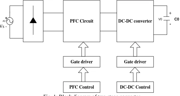
PFC Circuit DC-DC converter AC Gate driver PFC Control Gate driver DC-DC Control + -V0 C0 Vs -+
Fig. 1: Block diagram of two stage converter
II. DESIGN AND IMPLEMENTATION OF TWO STAGE AC-DC CONVERTER
Description
A boundary conduction mode (BCM) Boost power factor correction circuit is implemented. Compared to other topology the boost topology circuit requires the fewest external parts, the switch is source grounded, therefore easy to drive. Along with this the requirement of EMI filter is also minimized for this topology.
A fly back converter is used for DC-DC conversion. Compared to all other isolated converter fly back topology is simple. It is operated in discontinuous mode of operation (DCM). For low power application DCM mode is most commonly used.
Design of AC-DC Converter
Boost Power Factor Correction Circuit
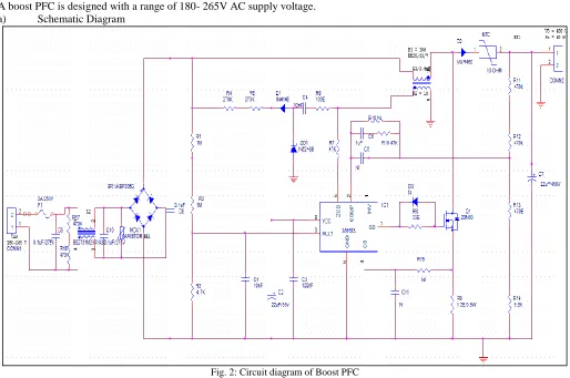
A boost PFC is designed with a range of 180- 265V AC supply voltage. a) Schematic Diagram
Fig. 2: Circuit diagram of Boost PFC
The complete schematic diagram of Boost PFC converter is shown in Fig. 2. A boost PFC operating in transition mode converts an ac supply voltage having the range of 180V- 235V is rectified by a bridge rectifier and the rectified voltage is delivered to the boost converter. By using a switching technique, the converter boosts the rectified input voltage to a regulated DC output voltage of 400V and also it shapes the input current in phase with input voltage in sine wave. A L6562A IC is used for PFC controller. b) Input specifications
Supply mains voltage range (Vac rms) Vac min = 180V
Vac max = 265V
Minimum mains frequency =47hz
Rated output power = 50W
Regulated DC output voltage (Vdc) = 400V
Expected efficiency = 94%
Expected PF = .95
c) Design Parameters
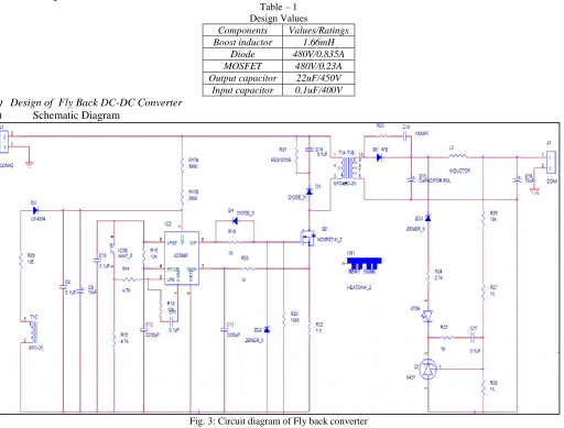
Table – 1 Design Values
Components Values/Ratings Boost inductor 1.66mH
Diode 480V/0.835A MOSFET 480V/0.23A Output capacitor 22uF/450V Input capacitor 0.1uF/400V Design of Fly Back DC-DC Converter
a) Schematic Diagram
Fig. 3: Circuit diagram of Fly back converter
A design of fly back converter operated in the switching frequency of 100 KHz with DCM mode of operation is shown. Since the input to the fly back converter is 400V dc, the design of fly back transformer is simple and has more efficiency compared to traditional fly back converter operated in AC supply.
b) Design Parameters
The major components of fly back converter are flyback transformer, output diode, input capacitor, output capacitor, MOSFET etc. The designed values of major components are described in table.
Table – 2 Design Values
Components Values/Ratings
Flyback transformer
EFD 25 Core N1/N2 =90/15 Primary inductance=2.3mH
Diode 480V/0.835A
MOSFET 700V/2A
Output capacitor 10uF/63V Input capacitor 0.1uF/1KV Arrangement of LED driver with PIC Micro Controller
Fig. 4: Arrangement of LED Array
In order to obtain PWM dimming a PIC micro controller of 18F2520 is used. A PIR sensor and LDR sensor is used as the input to the PIC micro controller. According to the signals generated from the sensors a PWM signal is generated by microcontroller and is given to the DIM pin of the LED driver.
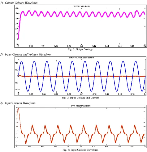
III. SIMULATION RESULTS
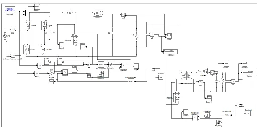
The purpose of the simulation is to investigating the operation mechanism of the converter and confirming the resultant waveforms with analytical calculation. The circuit shown in Fig.5 has been simulated in MATLAB, which is the closed loop simulation of two stage AC-DC converter. The simulation results are shown Fig.6, 7 and 8. The operating switching frequency is 100 kHz. As Fig.7 shows the input current tracks the input voltage, the power factor is almost unity. Output voltage is regulated at 48V. The simulation is done for 50W AC-DC converter.
Simulation Results
Output Voltage Waveform
Fig. 6: Output Voltage
Input Current and Voltage Waveform
Fig. 7: Input Voltage and Current
Input Current Waveform
Fig. 8: Input Current Waveform
Analysis of Simulation Results
The closed loop simulation of two stage AC-DC converter is done in MATLAB using Simulink model. The component values used in model is taken from the designed values of AC-DC converter. The output voltage of Flyback topology is 48V with less ripple. The input voltage and current are in phase and sinusoidal, so that the converter will achieve a better power factor.
IV. EXPERIMENTAL SETUP AND HARDWARE RESULTS
Hardware Results
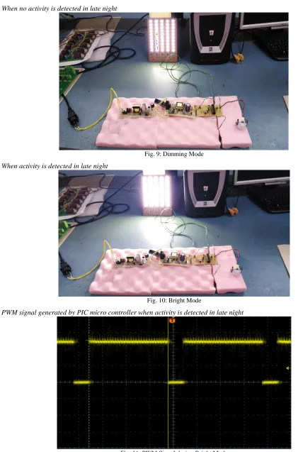
When no activity is detected in late night
Fig. 9: Dimming Mode
When activity is detected in late night
Fig. 10: Bright Mode
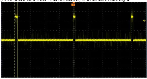
PWM signal generated by PIC micro controller when no activity is detected in late night
Fig. 12: PWM signal during dimming mode
Analysis of Hardware Results
The hardware results show that the energy consumption during late night can be reduced. Around 3 watts of energy is consuming during dim mode. This will save the energy.
V. CONCLUSION
This paper has proposed a two stage power-processing ac–dc converter with a high power factor and high power efficiency. The proposed converter has low line current harmonics and it achieves a power factor of about 0.997. And an overall efficiency of 86% is obtained.
Also, analysis, design, and experimental results for the pro-posed converter have been presented. The converter combines the full-bridge diode rectifier, a Boost PFC circuit and fly back dc–dc converter.
From hardware results the wastage of energy can be reduced and the energy efficiency can be achieved. By this proposed work, the calculation shows that a 50W of power is used during high brightness and in dim mode only 3W of power is consuming. This result shows how much amount of energy can be saved. The proposed system can autonomously adjust the minimum light intensity value to enhance both energy efficiency and user satisfaction. The main advantage of the proposed system is power saving. It requires the initial cost only for designing and installation and not for utilization. Hence this type of systems is very much useful for the government to reduce the utilization of conventional power.
REFERENCES
[1] S. K. Cho and V. Dhingra, “Street Lighting Control Based on Lon Works Power Line Communication,” IEEE International Symposium on Power Line
Communications and Its Applications Jeju City, 2-4 April 2008, pp. 396-398
[2] Zhang and J. W. Spencer, “Analysis of boost PFC converters operating in the discontinuous conduction mode,” IEEE Trans. Power Electron.vol. 26, no. 12,
pp. 3621–3628, Dec. 2011.
[3] C. Qian and K. M. Smedley, “A topology survey of single-stage power factor corrector with a boost type input-current shaper,” in Proc. IEEE Appl. Power
Electron. Conf. (APEC), pp. 460–467, Feb. 2000
[4] J. P. M. Figuerido, F. L. Tofili, and B. L. A. Silva, “A review of single-phase PFC topologies based on the boost converter,” in Proc. IEEE Int. Conf. Ind.
Appl., Sao Paulo, Brazil, pp. 1–6, Nov. 2010.
[5] T. Komine and M. Nakagawa,“Fundamental analysis forvisiblelight communication system using LED lights,”IEEE Transactions on Consumer Electronics
, vol. 50, no. 1, pp. 100 - 107, Feb. 2004.
[6] “A New Streetlight Monitoring System Based On Wireless Sensor Networks” IEEE 2010- GongSiliang
[7] “Optinal design of switching Power supply” by zhanyou sha, xiaojun wang, hongtao ma, text book
[8] AN2761Application note “Solution for designing a transition mode PFC preregulator with the L6562A”
[9] Fairchild application note AN-8035 “Design Consideration for Boundary Conduction Mode Power Factor Correction (PFC) Using FAN7930”
[10] C. Qiao and K. M. Smedley, “A topology survey of single-stage power factor corrector with a boost type
input-current-shaper,” IEEE Trans. Power Electron., vol. 16, no. 3, pp.360–368, May 2001.
[11] Q. Zhao, F. C. Lee, and F. Tsai, “Voltage and current stressreduction in singlestage power factor correction acdc
converters with bulk capacitor voltage feedback,” IEEE Trans. Power Electron., vol. 17, no. 4, pp. 477 -483, July 2002.
[12] Spiazzi, S. Buso and G. Meneghesso, “Analysis of a high-powefactor electronic ballast for high brightness light
emitting diodes,” IEEE Power Electronics Specialists Conference (PESC) Proc., pp. 1494 - 1499, 11,14 Sept.2005.