Author for correspondence:
Department of Computer Science Engineering, Nandha Engineering College
Volume-7 Issue-2
International Journal of Intellectual Advancements
and Research in Engineering Computations
Aggressive voltage and temperature control for power saving in mobile
application processors
Dr.D.Vanathi
1, Nathanial Alexander A
2, Naveen Kumar.P
2, Ramesh. A
21
Professor, Department of Computer Science and Engineering, Nandha Engineering College
2
UG Students Department of Computer Science and Engineering, Nandha Engineering College
ABSTRACT
DVFS may be a wide used methodology for reducing the facility consumption of mobile devices. This theme involves frequency scaling in accordance with a selected governor and therefore the institution of associate degree operational voltage to be paired with frequency. Incorporated into the settings for operational voltage may be a guard band that ensures safe processor operation even at the worst conditions of on-chip temperature. Typically, the processor temperature remains at a traditional vary (i.e., not the worst), thus the voltage a guard band set to ensure safe operation is excessively protected. During this paper, we tend to propose a temperature-aware DVS (T-DVS) that sharply reduces voltage guard band. We tend to explore the chance to supply minimum operational voltages for frequencies at completely different temperatures and notice a dynamic voltage management theme that reduces power consumption. The T-DVS manages temperature so it remains within the “green zone” where vermouth voltage gain is enabled for power-efficient operation. we tend to validate the effectiveness of the T-DVS beneath varied thermal conditions by mistreatment mobile application processors and completely different operational eventualities. Experimental results show that the T-DVS ends up in power gain while not degrading performance not with standing herbal conditions and chip characteristics. B y examining the real-world applications of and ready-to-wear smartphone, we tend to show that the voltage gains generated by the T-DVS leads to battery life increment.
Index Terms:
DVFS; Power Consumption; Temperature; Voltage Guard bandINTRODUCTION
Recently developed mobile devices employ high performance multicore application processors (APs) that provide complex functionalities. In these devices, performance increment is accompanied by additional power consumption, which constrains energy efficiency. Given that power optimization is a key issue in mobile device design and use, diverse methodologies have been developed to reduce power consumption. One such methodology is dynamic voltage and frequency scaling
(DVFS), which is a widely employed scheme that involves frequency scaling via a specific governor in an AP. The primary functionality of DVFS is the adequate selection of frequencies for power aware system operations. Here,
operating voltage is paired with a selected frequency. In most cases, voltage settings encompass a guard band that ensures stable execution under various operating conditions, such as temperature, voltage noise, IR drop, and circuit aging. Given that a guard band is set conservatively to support worst-case operating conditions, it can serve as an excess energy source in cases where in the aggressive addressing of power issues is required in mobile devices.
guaranteed on chip temperature1 usually ranges from –25 to 125°C. In conventional DVFS, a thoroughly tested unique voltage is adopted for each frequency in this temperature range. This unique voltage should be appropriate for safe system operation at all temperature ranges including the worst-case temperature. In other words, a voltage guard band should enable operations under the most inferior temperature conditions. In general use cases of mobile devices, however, the on-chip temperature in an AP remains at a normal range (i.e., not the worst) most of the time, and power consumption by a guard band that is intended to guarantee safe voltage is potentially wasteful.
If a guard band can be adjusted dynamically depending on temperature, the difference between adjusted and original voltages (i.e., voltage gain) can contribute to power saving. Previous research have attempted to reduce operating voltages by minimizing guard bands via diverse techniques, such as dynamic voltage reduction through error correction [4, 5], and guard band reduction with predictions of the voltage noise caused by program behavior [6]. Despite the insights provided by these studies, however, they failed to consider temperature issue
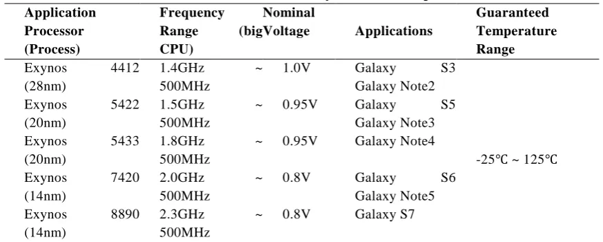
Table 1: Overview of Exynos Series of Aps Application
Processor (Process)
Frequency
Range (big
CPU)
Nominal
Voltage Applications
Guaranteed Temperature Range
Exynos 4412
(28nm)
1.4GHz ~
500MHz
1.0V Galaxy S3
Galaxy Note2
-25℃ ~ 125℃
Exynos 5422
(20nm)
1.5GHz ~
500MHz
0.95V Galaxy S5
Galaxy Note3
Exynos 5433
(20nm)
1.8GHz ~
500MHz
0.95V Galaxy Note4
Exynos 7420
(14nm)
2.0GHz ~
500MHz
0.8V Galaxy S6
Galaxy Note5
Exynos 8890
(14nm)
2.3GHz ~
500MHz
0.8V Galaxy S7
With this consideration in mind, we endeavor to acquire voltage gain by minimizing the voltage guardband2 that is conservatively provided for the worst temperature; for this purpose, we examine the relationship between on-chip temperature and operating voltage on the basis of temperature inversion. As indicated by the temperature inversion phenomenon, the minimum operating voltage, change son the basis o fon- chip temperature. Hence, the temperature voltage relationship enables dynamic guard band control and provides an opportunity to reduce power consumption. We also explore the optimal on chip temperature at which voltage gain is maximized. We define the optimal on-chip temperature by observing the temperature inversion phenomenon occurring in commercial mobile APs and call the optimal temperature range the “green zone”. To achieve these goals, we seek solutions to two challenging problems: ensuring dynamic voltage control with
temperature and providing robustness to chip variation. First, we acquire the minimum operating voltage, i.e., the minimum voltage to secure the system operation at various operating conditions, at runtime for various on chip temperatures, and aggressively control temperature to induce the maximum voltage gain while maintaining accurate system operation. Second, we develop a pragmatic solution that compensates for various chip characteristics to ensure the robustness of the solution. Specifically, we propose a temperature-aware DVS (T-DVS) as a means of addressing the aforementioned problems.
The contributions of our work are
summarized as follows
temperature toward the green zone for power efficient system operation with maximum voltage gain. We demonstrate that the T-DVS operates adequately on commercial APs and that a rescaling of voltage reduces power consumption. To the best of our knowledge, our scheme is the first work that handles the temperature issues aggressively to reduce voltage guard band. Although power reduction is an important issue for mobile devices, it should not be achieved at the expense of performance, whose degradation eventually causes a decline in the quality of service (QoS) for user. The solution put forward in this work preserves operating performance while reducing power consumption.
We confirm that temperature-aware guard band voltage reduction is feasible on the basis of observations of the temperature voltage relationship.
We propose the green zone concept and validate its efficacy for power reduction.
We implement a prototype T-DVS system, and evaluate its effectiveness through various experiments using off the helf AP chips and smartphone.
TEMPERATURE INVERSION
PHENOMENON
All clock-driven semiconductors are designed to satisfy a target frequency with a driving voltage called the process nominal voltage. Engineers ought to find ways to achieve the target frequency operation at the given process nominal voltage. Mobile APs typically operate over a wide frequency range, including the design target frequency. The available frequency range is determined by a characterization test conducted after chip manufacturing. Overdrive refers to the case wherein a frequency and a voltage higher than the design target frequency are used, where asunder-drive pertains to the opposite case. As indicated by the temperature inversion phenomenon, the minimum voltage level that drives silicon circuits changes in accordance with circuit temperature. In overdrive, the operating voltage must be increased when temperature rises. In under drive, this voltage can be reduced when temperature increases.
To reproduce temperature inversion in an actual device, we conducted experiments using commercial APs. The experiments involved measuring the of a CPU at various on-chip temperatures and observing the changes in 𝑉𝑚𝑖𝑛. The voltage noise, temperature, IR drop, and circuit aging are the key operating conditions that influence the operating voltage. In our experiment, Vmin was measured by running dynamic work loads repeatedly while the voltage level is gradually decremented till a system error occurs. We used four different mobile APs, namely, Samsung Exynos 4412, 5433, 7420, and 8890.Table 1 provides an overview of the Exynos series. Exynos 4 and 5 are manufactured using 28- and 20-nm processes and run with nominal voltages of 1.0 and 0.95V, respectively. Exynos 7 and 8 are manufactured with a14-nm.
T-DVS SYSTEM
The T-DVS enables aggressive voltage and temperature control for power conservation. In the preceding experiment, we observed that alters depending on chip variations and that its effect is maximized at the greenzone. In applying the T-DVS, therefore, we should consider the characteristics of individual chipsets in estimates of voltage gain and endeavor to direct temperature toward the green zone. To this end, the proposed scheme allows for adaptive control of voltage and temperature, and considers chipset characteristics.A voltage gain learner, a runtime temperature checker, a temperature controller, and a DVS controller. The voltage gain learner obtains the coefficient that represents the various characteristics of chipsets. The runtime temperature checker measures CPU temperature at runtime via the thermal sensors in an AP. The temperature controller drects temperature toward the green zone, thereby maximizing the effect of voltage gain. The DVS controller chang- es voltage with reference to given parameters, such as frequency, temperature, and coefficient of chip characteristics.
Voltage Gain Learning
operating voltage for each chip necessitates that the individual characteristics of the temperature voltage relationship be determined in advance. The best way to derive an accurate representation of the relationship is to test all available frequencies at various temperature conditions. This approach, however, is practically not possible given the cost and time required for such testing. We instead built a model that represents the temperature voltage relationship and performed minimum testing to obtain the coefficients for the model. We incurred negligible test cost and overhead with this approach. The actual relationship between voltage and temperature depends on many parameters, and a model that represents all the parameters is necessarily complex. Such model is inapplicable to our context, in spite of its accuracy, again because of test cost and time constraints.
We were compelled to build the simplest model possible and decided on a linear model. Specifically, the Pearson’s correlation coefficient [11] was used to measure the linear correlation between two variables, and the temperature- voltage model was validated accordingly. Using the results of the temperature inversion experiment, we calculated the Pearson’s correlation coefficient which indicates the line aristov 𝑚𝑖𝑛 with respect to on-chip temperature. For all the Exynos APs, the coefficients are greater than 0.84, and the overall averagecoefficientsofExynos4412, 5433, 7420, and 8890 are 0.9351, 0.9220, 0.9494, and 0.9160, respectively. The coefficients indicate high linearity of data and support model and the actual relationship is compensated by the actual
voltage output of PMIC, which is set at regular intervals, i.e., the voltage control step [12]. The compensated voltage reinforces the stability of the control scheme. Voltage gain learning is conducted in the chip manufacturing phase to acquire voltage gain, with the acquisition considering variations in the semiconductor process. A semiconductor manufacturing line provides an ade- quate environment for voltage gain learning because the test equipment used in the manufacturing phase enables consistent temperature control. Note that a favorable approach to learning about the voltage gain of each chipset is to do so at runtime on actual devices (e.g., during boot time), but consistent temperature management is difficult during test. First, the four s, namely, VH1, VH2, VL1, and VL2, are measured at four different temperatures, namely, t1, t2, t3, and t4, respectively. That is, the lowest frequency, is measured at low temperature t1; the highest frequency, is measured at low temperature t2 is measured at high temperature t3is measured at high temperaturet4.We checked the latency of voltage gain learning in the chip manufacturing phase for all the Exynos APs. An average latency of 90 ms is required to acquire and approximately400msisnecessaryfortheoveralltest ingof voltage gain learning for a chip. Considering that the test time of a system on chip in the manufacturing phase.
Temperature Controller
Temperature Checker
The runtime temperature checker monitors changes in on-chip temperature in real time and correspondingly notifies the DVS controller, thereby avoiding unstable situations due to rapid temperature changes. Abrupt changes in on-chip temperature occur frequently in high performance APs, and the time required to take action for these changes is shorter than the default DVFS interval in a normal Android system. Independent temperature checking is therefore safe and preferred over synchronization with the DVFS interval for three CPU intensive bench- marks: the Antutu benchmark for Android, Geek Bench for Android, and the repetitive firmware- based ZipUnzip benchmark. The CPU test for Antutu and GeekBench registers a fast temperature increment at about 15 and 22 °C in 200 ms, respectively. The test for the firmware-based ZipUnzip benchmark shows an even faster temperature increment at almost 20 °C in 100 ms. Although the test was designed to intentionally increase on-chip temperature, it also shows the possibility of fast temperature increments on high-performance mobile devices. On the basis of the results, the interval for temper aeration is illustrated. If the current temperature is below the green zone threshold (i.e., green Threshold_ temp), the temperature controller starts to increase on-chip temperature by elevating operating frequency. When the current temperature exceeds green Thres hold temp, the temperature controller does not affect system operation. That is, the system remains safe since the voltage gain is increased while temperature changes toward the green zone. The green Threshold temp is as signed a constant
value in our work to evaluate the scheme. In our future work, we intend to determine other green Threshold temp values by using feedback from data on runtime voltage gain.
DVS Controller
EVALUATION
We conducted experiments to evaluate the functionalities and effectiveness of the T-DVS. To validate the functionalities, chip-level tests were performed using commercial APs. Specifically, a firmware-based test and an Android- based real-world application test were carried out. To evaluate effectiveness, system level tests that involved Android based real-world application scenarios were performed on an off-the-shelf smartphone. Experimental Setup To validates T-DVS functionality, we set up chip-level tests using the Exynos 5433 AP, which employs the big. LITTLE CPU architecture. The highest and lowest operating frequencies of the big cores are 1.9 GHz and 800MHz, respectively. Through the tests, we validated the following key functionalities:
𝑉𝑚𝑖𝑛estimation with voltage gain learning, acquisition of voltage gains at various conditions, and temperature control with respect to the green zone. The tests were performed on the AP evaluation board with the AP tester shown in. The AP evaluation board was designed to evaluate APs and provides multiple points from which to measure power and voltage for every power domain of an AP. Voltage change and power consumption are readily captured using the measurement points on the board. The on-chip tempera ture of an AP can also be collected by reading the registers of the thermal sensors embedded in the AP. The AP tester
enables multichip testing with programmable test scripts that control chip handling, power supply, and ambient temperature for an entire test. Here, the ambient temperature does not represent the semiconductor characteristics directly, yet affects the on-chip temperature changes as an environmental factor. In our work, we conducted experiments with an ambient temperature control to emulate various thermal conditions that are similar to real operating environment for mobile devices. The AP tester can control ambient temperature with one degree of temperature resolution. Note that fine-grained temperature control is important for the validation of the T -DVS functionalities. Accuracy of Estimated Voltage The accuracy ofis crucial to estimating, ensuring the stability of the proposed solution. In the event of an erroneous decision, an inappropriate immediately causes a system malfunction. To validate the accuracy of estimation, we conducted experiments by running a firmware-based CPU memcopy test on the Exynos 5433 and 7420 APs.
that the maximum values of the five measured
𝑉𝑚𝑖𝑛values constitute the oracle. The scenario featured repetitive one minute long touch and scroll actions on the Android 4.4 menu screen. The ambient temperature was room temperature, and no external temperature control was applied. shows the trace results. The dotted line denotes the oracle voltage, and the grey line represents the set voltage that was estimated by the T-DVS and compensated with the PMIC voltage step. Given that the oracle voltage is the base line for safe operation
Voltage Gain
The T-DVS enables voltage gain as a result of estimation and leads to power saving. To validate that the voltage gains were acquired correctly by the T-DVS, we conducted an experiment with a Monkey script based test scenario run on Android 4.4.
The script consists of three simple actions: menu screen scroll, web browsing with the default browser, and text typing with the default SMS application. We consider that the repeated operation of these applications would represent smartphone users’ usual behavior and encompass typical workloads. The experiments were performed at three ambient temperatures (i.e., cold, room, hot) controlled by the AP tester to observe the voltage gains at different temperature Condi voltages indicate how much voltage gain is obtained for each frequency at a specific temperature condition. The black bars in the graph are default voltages without the T-DVS, and the five colored bars indicate the voltages of five chips with the T-DVS.We found a difference in the voltage gains of all frequencies between temperature conditions. For reference, the average on-chip temperatures
under the cold, room, and hot conditions were 12, 41, and 78 °C, respectively. At a high temperature, the voltage gain at a low frequency is higher than that at a high frequency. This situation is reversed at low temperatures. The different on- chip temperatures lead to different voltage gains a dissimilarity that coincides with the phenomenon of temperature inversion. We also found a difference from the experimental results that seems to have resulted from chip variation. Chip #1 exhibits higher voltage gains than those generated by others at high frequencies, whereas Chip #5 exhibits higher voltage gains than those derived with others at low frequencies. This phenomenon can be explained using the leakage current characteristics of the chips.
Frequency in most cases and high frequencies for specific events, such as a touch action. With this result, we consider that the voltage gain derived by the T-DVS can contribute to power saving in real-world applications of mobile devices.
Temperature Change
The temperature controller module of the T-DVS directs temperature toward the green zone when the current temperature is lower than the green zone threshold. When the temperature controller runs correctly, a change in on-chip temperature is expected. Again, we conducted an hour long Monkey script-based test and captured the on-chip temperature of a CPU. Because the temperature controller operates only when the on-chip temperature is low, we configured the ambient temperature to cold (0 °C). In other words, this test emulates green zone evaluation under the assumption that a device is exposed to cold temperature. The on-chip CPU temperature
was measured every second, and the green zone threshold was configured to 20 °C. The results show that temperature allocations in the green-zone increase by about 15% when the temperature controller is operational (i.e., white bar in the figure), whereas low temperature allocations decrease. At a high temperature, no significant change was observed. This means that as expected, the temperature controller of the T-DVS directs low temperature toward the green zone at a low temperature range and directs temperature toward the green zone.
Power Consumption
The voltage gain achieved by the T-DVS results in direct power reduction. We conducted an experiment to check how much power is reduced by the T-DVS. Given that we implemented the T-DVS only in a CPU, we measured CPU power consumption with the AP evaluation board.
For the test, we used the GeekBench3 benchmark application. Note that Geekbench3 can increase the CPU workload to a maximum level, hence enabling the observation of power saving effect of T-DVS under high CPU power consumption. The test was performed at three ambient temperatures (cold, room, and hot) and three conditions, namely, DVS disabled, T-DVS without the green zone scheme, and T-T-DVS functionality enabled including the green zone scheme. When the entire T-DVS is enabled, the power consumptions are lower than those without T-DVS application by 8.6%, 10.9%, and 9.6% at the cold, room, and hot temperatures, respectively. More effective power reduction is
achieved at room temperature than at the other temperatures. When the T-DVS is enabled without the green zone scheme, power reductions are 6.6%, 11.0%, and 9.6% at the cold, room, and hot temperatures, respectively. The incorporation of the green zone scheme results in about 2% more power reduction at the cold temperature. The power saving effect of the green zone scheme is not significant with the current implementation.
excluding high temperature range, in order to prevent the performance degradation caused from frequency decrement. We, however, believe that power saving by the green zone scheme could be achieved significantly if temperature control is performed at the high temperature range with the help of effective cooling method, such as the use of a cooling fan with dynamic speed controller. In summary, our experiment results indicate that the voltage gain achieved by the T-DVS leads to power saving and that the power saving effect of the T-DVS can be improved if on-chip temperature is maintained at the mid-point range by using the green zone scheme. Assuming that mobile devices are mostly used at mid-range temperature, users are expected to realize approximately 10%of CPU power saving with the T-DVS. Performance difference over the baseline (Geekbench 3 benchmark).Meanwhile, in order to show that T -DVS achieves power saving without degrading performance, we conducted additional experiments. We consider that benchmark applications are the good means to compare the performance because the benchmark scores represent the performance directly. Again, the evaluation was conducted with GeekBench3. We acquired the results for three cases, i.e., the baseline, T-DVS without the green zone, and T- DVS with the green zone. performance difference is within the experiment error of 0.4%. The difference varies slightly in every repetition, yet not over 0.4% for overall measurements.
Overall, T-DVS is shown to achieve power saving with negligible performance degradation-DVS Overhead We calculated the runtime overhead generated by the T- DVS. The runtime overhead originates from the temperature checker, which runs every 10 ms, and the DVS controller, which is invoked if a temperature or frequency change is detected. The overall execution time of the temperature checker and DVS controller is 45 µs with the lowest CPU clock. This value corresponds to 0.45% of CPU runtime and is a negligible over head. Improvement in Battery Lifetime In the real world, battery lifetime increment is an indicator of the effectiveness of a power saving mechanism. We conducted experiments to understand the extent of battery lifetime improvement that is achieved by the T-DVS. We
used an Exynos 5422 AP-based Galaxy S5 and wrote Comparison of battery lifetime of the Galaxy S5 smartphone with repetitive Android real-app Monkey script test. Test cases.
The default battery lifetime without the T-DVS is 7 hours, 11 minutes, and 21 seconds. With the T-DVS enabled, the smartphone runs for 7 hours, 33 minutes, and 42 seconds. This improvement in battery lifetime corresponds to 22 minutes or 4.9% with T-DVS application. Although this increment is a minor enhancement, a notable issue is that additional battery lifetime is obtained with only a software change and without a decline in performance. We also determined the voltage gains derived during the test to check how much voltage gain would be realized by the T-DVS. Shows that voltage gains are acquired during the entire lifetime of the battery. The average voltage gain is close to 12.5 mV. The voltage gains were applied to the PMIC voltage step at one (12.5 mV) to three (37.5 mV) steps. The sustainable voltage gain means that the T-DVS runs continuously, regardless of system operation conditions. We also conducted an aging test to observe whether the T-DVS runs stably on a smartphone and does not harm system operation for an extended period. We used a Galaxy S5 with a DC power supply as a substitute for the battery and ran the same Monkey script. The aging test ran for two weeks without presenting any functional problems.
RELATED WORK
Choietal. strengthened the scheduling algorithm for DVFS with thoughtful workload analysis. Many other studies have attempted to optimize frequency to reduce power consumption while preserving performance.
Although DVFS was improved, voltage scaling remained a passive component since frequency scaling is the dominant factor ofDVFS.A few recent works centered on voltage optimization. Bacha et al. achieved dynamic voltage reduction using on-chip error correction code based voltage speculation. A benchmark test with a specific firmware demonstrated that approximately 20% power conservation is possible with aggressive voltage reduction over Intel’s Itanium processor. Leng et al.endeavored to reduce the voltage guard band that is incorporated in conventional GPU operation. The authors pointed out that the guard band for voltage noises stems from various program behaviors and optimized the guard band with off-the-shelf GPUs used in desktops. The study, however, underrated the influence of temperature on guard band a tendency that was motivated by the fact that a desktop is equipped with a strong cooling system. Mobile devices have no explicit cooling control system, and temperature typically affects device power consumption significantly.
With respect to thermal management in mobile devices, Brooks et al. and Kumar et al. emphasized the importance of thermal management. Many studies supported this perspective. DTM is an advanced thermal management system that is used to protect systems from thermal damage. Kimetal. and Leeetal. Studied temperature-aware DVFS aimed at enhancing DTM through the effective management of temperature with frequency control. In general, frequency optimization is accompanied by performance degradation, which is an undesirable outcome. By contrast, voltage optimization does not affect system performance
a major benefit provided by the T-DVS. Recently, Mercatietal. focused on the temperature issue on semiconductor reliability. The proposed WARM scheme controls temperature dynamically to preserve the reliability of semiconductors, leading to lifetime increment. T-DVS, in contrast, controls temperature to improve power efficiency. Meanwhile, near threshold voltage (NTV) technology emphasizes the importance of reduced operating voltage. Kauletal introduced the concept of NTV and demonstrated that maximum energy efficiency can be achieved using this technology. Intel demonstrated the effectiveness of an NTV Pentium processor that runs on very low power. Voltage down using software techniques facilitates the NTV scheme. We expect the T-DVS to drive the development of techniques that center on reducing operating voltages and exerting synergistic effects on technologies such as NTV. In the case of combined use of the T-DVS and other methods, benefits will be retained without any loss.
CONCLUSION
We incontestable that the T-DVS can do power saving with aggressive voltage management by capitalizing on the connection between operational voltage and temperature. we tend to expect the T-DVS to line a milestone in active voltage management for power management in mobile devices. The effectiveness of the T-DVS was achieved only by mistreatment code approaches and using existing hardware options. If AP makers develop further hard- ware options that facilitate the T-DVS, the planned theme would become additional powerful and convenient. within the gift work we tend to valid the theme with solelyhuge hardware cores, however we tend to commit to extend the theme to alternative hardware parts of Aps.
REFERENCE
[1]. J. Park and H. Cha, “T-DVS: Temperature-aware DVS based on temperature inversion phenomenon,” in Proc. Int. Symp. Low Power Electronics and Designs (ISLP ED’16), 2016, 248-253
[2]. M.Halpern, Y.Zhu, and V.Reddi,“Mobile CPU’ sriseto power: Quantifying the impact of generational mobile CPU design trends on performance, energy, and user satisfaction,” in Proc. IEEE Int. Symp. High Performance Computer Architecture (HPCA ’16), 2016, 64–76.
doi:10.1109/HPCA.2016.7446054.
[4]. A. Bacha and R. Teodorescu, “Dynamic reduction of voltage margin by leveragingon-chipECCinItaniumIIprocessor,”inProc.40thAnnu.Int. Symp.Computer Architecture (ISCA `13), 2013, 297–307, doi:10.1145/2485922.2485948.
[5]. A. Bacha and R. Teodorescu, “Using ECC feedback to guidevoltage speculation in low-voltage processors,” in Proc. 47th Annu. Int. Symp. Microarchitecture (MICRO ’14), 2014, 306–318.
doi:10.1109/MICRO.2014.54.
[6]. J. Leng, A. Buyuktosunoglu, R. Bertran, P. Bose, and V. Reddi, “Safe limits on voltage reduction efficiency in GPUs,” in Proc. 48th Int. Symp. Microarchitecture (MICRO ’15), 2015, 294 –307. doi:10.1145/2830772.2830811.
[7]. W. Lee, Y. Wang, T. Cui, S. Nazarian, and M. Pedram, “Dynamic thermal management for FinFET -based circuits exploiting the temperature effect tinversion phenomenon, ”in Proc.Int. Symp. Low Power Electronics and Design (ISLPED ’14), 2014, 105–110, doi:10.1145/2627369.2627608.
[8]. A. Edman and C. Svensson, “Timing closure through aglobally syn- chronous, timing partitioned design methodology,” in Proc. 41st Annu. Design Automation Conf. (DAC ’04), 2004, 71 –74. doi:10.1145/996566.996586.
[9]. P. Gronowski, W. Bowhill, R. Preston, M. Gowan, and R.Allmon, “High-performance micro processor design,”IEEEJ.Solid- State Circuits, 33(5), 1998, 676–686.
[10].N.Kim,T.Austin, D.Baauw, T.Mudge, K.Flautner, J.Hu,M. Irwin,M. Kandemir, and V. Narayanan, “Leakage current: Moore’s law meets staticcurrent,”IEEETrans.Comput.,36(12), 68-75, 2003.
[11].J. Benesty, J. Chen, Y. Huang, and I. Cohen, “Pearson correlation coeffi- cient,” Noise Reduction in Speech Processing, Springer Topics in Signal ProcessingSeries,12, 2009, 1–4.
[12].Samsung Electronics Co. Ltd. “S2MPS11_PMIC_Datasheet,”2014.
[13].D. Gizopoulos, A. Paschalis, and Y. Zorian, Embedded Processor -based self- test. Springer Science & Business Media, DOI10.1007/978-1-4020-2801-4
[14].Antutu Benchmark, Antutu Labs, 2016. [15].Geekbench3,PrimateLabs 2016.
[16].K. Govil, E. Chan, and H. Wassermann, “Comparing algorithmsfor dynamic speed -setting of a low-power CPU,” in Proc. 1st Conf. Mobile Computing and Networking (MOBICOM ’95), 1995, 13–25. doi:10.1145/215530.215546.
[17].T.Pering, T. Burd, and R.Brodersen, “Thesimulation and evaluation of dynamic voltages calingalgorithm,” in Proc. Int. Symp. Low PowerElec- tronics and Design (ISLPED ’98), 1998, 76-81.
doi:10.1145/280756.280790.
[18].M. Weiser, B. Welch, A. Demers, and S. Shenker, “Scheduling forreduced CPU Energy,” in Mobile Computing, T. Imielinski and H. Korth, Eds., The Kluwer International Series, 1994, 449 –471. [19].F. Gruian, “Hard real-time scheduling for low-energy using stochastic data and DVS processors, “in
Proc. Int. Symp. Low Power Electronics and Design (ISLPED’01), 2001, 46–51. doi:10.1145/383082.383092.
[20].P. Pillai and K. Shin, “Real-time dynamic voltage scaling for low-power embedded operating systems,” in Proc. 18th Symp. Operating Systems Principles (SOSP ’01), 2001, 89–102.
doi:10.1145/502059.502044.
[21].J. Pouwelse, K. Langendoen, and H. Sips, “Dynamic voltage scaling on a low- power micro processor,” inProc.7thAnnu.Int.Conf.MobileCom- puting and Networking (MobiCom ’01), 2001, 251–259, doi:10.1145/381677.381701.
[22].K. Choi, R. Soma, and M. Pedram, “Dynamic voltage and frequency scaling based on workload decomposition,” in Proc. Int. Symp. Low Power Electronics and Design (ISLPED ’04), 2009, 174– 179, doi:10.1145/1013235.1013282.
[23].D. Brooks and M. Martonosi, “Dynamic thermal management for high-performance microprocessor,” in Proc. High-Performance Computer Ar- chitecture (HPCA ’01), 2001, 171–182.
[24].A.Kumar, L.Shang, L.Peh, and N.Jha, “System-level dynamic thermal management for high-performance microprocessors,” IEEE Trans. Comput.-Aided Design Integr. Circuits Syst., 27(1), 2008, 96–108, doi:10.1109/TCAD.2007.907062.
[25].J. Kim, Y. Kim, and S. Chung, “Stabilizing CPU frequency and voltage for temperature-aware DVF Sin mobile devices, ”IEEE Trans. Computer, 64(1), 2013, 286–292,Sep.,doi:10.1109/TC.2013.188. [26].J. Lee, K. Skadron, and S. Chung, “Predictive temperature-aware DVFS,’” IEEE Trans. Comput.,
59(1), 2009, 127–133, Sep. doi:10.1109/TC.2009.136.
[27].P.Mercati,F.Paterna,A.Bartolini,L.Benini,T.Rosing,“WARM:Work-load-aware reliability
management in Linux/Android”, IEEE Trans. CADo fIntegrated Circuit and Systems, 36(9), 2016, 1557-1570, doi:10.1109/TCAD.2016.2611501
[28].H. Kaul, M. Anders, S. Hsu, A. Agarwal, R. Krishnamurthy, and S. Borkar, “Near-threshold voltage (NTV) design: Opportunities and chal- lenges, ”inProc.49thDesignAutomation Conf.(DAC’12), 2012, 1153– 1158, doi:10.1145/2228360.2228572