Effect Of Annealing Temperature For CuO Thin
Films Properties Prepared By Simple Chemical
Methods
Alia A. Shehab and Maithm A. Aabed
Collage of Education for pure science, Ibn Al-Haitham University of Baghdad, Baghdad, Iraq Corresponding author: [email protected]
Abstract—In this work, copper oxide have been
prepared by chemical method and deposition as
thin films on glass substrates at different
annealing temperatures (as-prepared, 100, 200
,300) °C then, studied the effect of temperature on the structural properties, The structure of the
deposited CuO thin films characterized by X-ray
diffraction, Atomic Force Microscope AFM
(topographic image) showed that the surface
Characteristics, All thin films prepared appeared
as multi-polarization with type unilateral
inclination and direction of the prevailing (110),
increasing the size of Crystallography rate with
increasing temperature as well as the picture an
atomic force (AFM) showed that the values of
average particle size increase from (73.25nm) to
(nm106.93 ) also the values of the surface
roughness and the values of the square root and
the average square roughness (RMS) increases
with elevating of temperature, from observed the
rate values of granular size conclude appear some
compositions of nanoparticles on thin films.
Keywords—CuO, Thin Films, structure properties, AFM,
1. Introduction
Copper oxides are considered important
semiconductor of metal oxides, it nanomaterial
because have the benefit of a low surface potential
barrier which effects on electron field emission
properties. There are two types of copper oxide
formed from copper include : cupric (CuO) and
curprous (Cu2O) were p-type with narrow band
gap energy 1.21 to1.51 eV and 2.1 to 2.6 eV
respectively [1-3] Potential field emitter has been
copper oxide which a good gas sensing material
as well as an efficient catalytic agent. It also
perform an essential role in optoelectronics and
solar cell ]4-10[. It has recently studied
demonstrated the nature and their reasonably
good electrical and optical properties by Cu2O.
while CuO with different Nano shape has been
formed by different methods in many research
papers [11-17] CuO is attractive as a selective
solar absorber since it has high solar absorbency
and a low thermal emittance [18]. These oxides
can concur with copper, annealing Cu2O films in
air at 300oC converts it to copper oxide [19]. So,
the aim of study preparing CuO NPs using the
chemical reaction method and studies the
structural , topographical and optical properties.
2. Experimental
Re-distilled water was used throughout the
experiment. In a typical procedure, 1.5 g of
Cu(NO3)2.H2O (BDH Chemicals Ltd Pool
England) was dissolved in 50 mL of PVP (Sigma
Aldrich USA) 1 WT. %. The solution was added
into a round-bottom flask with stirring. The color
(1M) was rapidly added to the mixture, and a
Nano powder suspension was formed . The
suspension was kept at 75 °C for 1 h. A large
amount of black precipitate was produced. After
cooling to room temperature, the particles were
separated by centrifugation and were washed with
distilled water to remove any contaminations. The
particles were then dried in an oven at 80 °C.
Thin film deposition by drop casting method
Glass slides of (1.00 x1.50) cm2 area, were used
as a substrate. They were cleaned with alcohol in
an ultrasonic bath in order to remove the
impurities and residuals from their surface. 5
drops of the colloidal were used in preparing the
CuO thin films on glass by drop casting method
.The structural properties of the deposited thin
films at room temperature were studied by using
ray diffractometer (XRD-6000,Shimadzu
X-ray Diffractometer) The optical absorption of the
colloidal CuO NPs was measured using
spectrophotometer (CARY,100 CONC plus,
UV-Vis-NIR, Splitbeam Optics, Dual detectors) in the
range of (200-900nm), using quartz vessel. The
shape and size of CuO nanoparticles were
investigated by using AFM (A A 3000 Scanning
Probe Microscope)
3. Results and Discussion
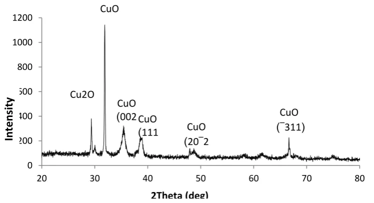
The XRD diffraction patterns of
synthesized CuO thin films deposited on glass at
as prepared are shown in figure (1). The XRD
patterns of CuO contain six main peaks at
diffraction angles : 29.400 , 31.908, 35.417,
38.714, 48.731 and 66.674 corresponding to
(110), (110), (002), (111), (20¯2) and (¯311)
planes .This result shown Cu2O at peak in
29.400, while other peaks shown CuO.
0 200 400 600 800 1000 1200
20 30 40 50 60 70 80
CuO
CuO )002 CuO
)111 CuO
)20¯2
CuO )¯311(
2Theta (deg)
In
tensit
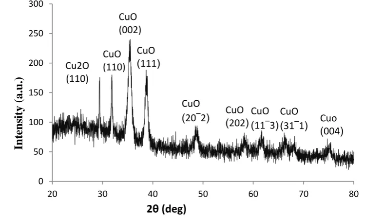
When at 100 °C the XRD patterns of CuO contain ten main peaks at diffraction angles:29.404, 31.856, 35.419, 38.737, 48.663,
58.200, 61.543, 66.262, 68.051 and 74.949. From figure 2 appear Cu2O at peak in 29.404 and remained peaks shown CuO.
Fig. 2. XRD pattern of CuO thin film at 100°C
At 200 °C the XRD patterns of CuO contain eight main peaks at diffraction angles: 29.462, 30.143, 31.921, 35.823, 38.914, 45.554, 48.468 and 66.687. Figure 3 illustrated the XRD pattern of Cu2O at peak in 29.404 and 30.143, and other peaks shown CuO.
Fig. 3. XRD pattern of CuO thin film at 200°C 0
50 100 150 200 250 300 350 400 450
20 30 40 50 60 70 80
CuO )110(
CuO )¯111(
CuO )200(
CuO )11¯2(
CuO )20¯2(
CuO )¯311( Cu2O
)110(
2θ (deg)
In
tensit
y Cu2O
0 50 100 150 200 250 300
20 30 40 50 60 70 80
CuO (110)
CuO (002)
CuO )111(
CuO
)20¯2( CuO)202(CuO )11¯3(
CuO
)31¯1( Cuo)004(
2θ (deg)
I
Intens
it
y
(a.u.)
The XRD patterns of CuO at 300 °C contain seven main peaks at diffraction angles:29.325, 29.763, 30.061, 31.811, 47.869, 62.586 and 66.582.This result
shown in figure 4 which refer Cu2O at peak in 29.325,29.763 and 30.061 while other peaks refer to CuO
Fig. 4. XRD pattern for CuO thin film at 300°C
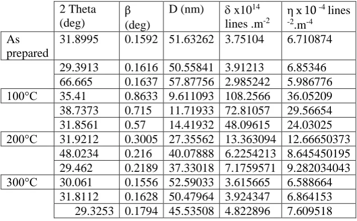
Tabel 1: parameters of XRD for CuO thin film at deferments annealing temperatures.
η x 10-4 lines
-2.m-4
x1014
lines .m-2 D (nm) β (deg) 2 Theta (deg) 6.710874 3.75104 51.63262 0.1592 31.8995 As prepared 6.85346 3.91213 50.55841 0.1616 29.3913 5.986776 2.985242 57.87756 0.1637 66.665 36.05209 108.2566 9.611093 0.8633 35.41 100°C 29.56654 72.81057 11.71933 0.715 38.7373 24.03025 48.09615 14.41932 0.57 31.8561 12.66650373 13.363094 27.35562 0.3005 31.9212 200°C 8.645450195 6.2254213 40.07888 0.216 48.0234 9.282034043 7.1759571 37.33018 0.2189 29.462 6.588664 3.615665 52.59033 0.1556 30.061 300°C 6.864153 3.924347 50.47964 0.1628 31.8112 7.609518 4.822896 45.53508 0.1794 29.3253
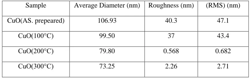
AFM depicts the surface morphology of the
copper oxide thin films analyzed by (AFM). The
surface of the (CuO) thin films as observed from
denser films significantly with the increased
temperatures. From the images ,it was observed
that the surfaces of the films exhibited ascertain 0 100 200 300 400 500 600 700 800
20 30 40 50 60 70 80
Cu2O )110(
CuO )110(
CuO )ത220(
CuO
)¯113( CuO)220(
grains with increasing temperatures leads to an
decrease in the surface roughness It is observed
that the average grain size decreases with
increasing of temperatures and the values of the
average grain size variable from (106-73) nm
depending on film temperatures as shown in
presented in Table (1) .. The average grain size
results (listed in Table) disagree with those
estimated from XRD due to the fact that the AFM
measurement directly visualizes the grains The
results obtained from the (AFM) of the
nanostructure for different temperatures as of
(CuO) thin film show that the histogram of the
percentage of (CuO) as a function of the grain size
are shown in figure (2). From this figure, the
percentage of minimum grain size were
(130-362)% for film temperatures of (as,100,200
and300) C° respectively. Also, it is clear from the
figure, that the average grain size were (106,
99,79 and73) nm with for the previous
temperatures. This structural films are very
important for many novel applications such as
optoelectronic devices, gas sensors and biological
science.
Table 2: characterization on CuO thin films
(RMS) (nm) Roughness (nm)
Average Diameter (nm) Sample
47.1 40.3
106.93 CuO(AS. prepeared)
43.4 37
99.50 CuO(100°C)
0.682 0.568
79.80 CuO(200°C)
2.71 2.26
Fig. (5)AFM images of CuO thin film
FTIR analysis of CuO nanoparticles
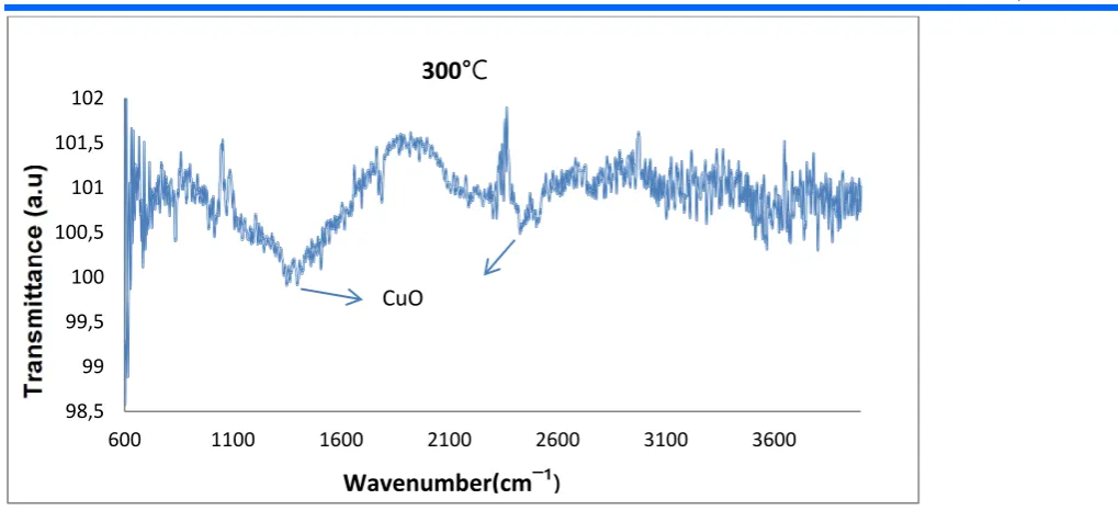
From FTIR data as shown in Figure (6) for PSi
/p-Si respectively, synthesized by 15 mA/cm2
etching current density and different etching
times, clearly there are three distinct peaks with
different intensities. The peak with intensity at
1080 indicates the presence of Si-O-Si wagging.
A a small peak at 624 can be associated with the
Si-H Waggener mode. While a peak at 2854
suggests the C-H stretching. A strong broad band
is observed at about 1080 due to Si-O-Si
asymmetry stretching vibrations mode in p-Si and
n-Si type. The weak absorption bands centered at
the species. Absorption at 2854 and 2924 is due
to the plane C–H angle deformation.It can easily
replace a silicon atom, leading to the presence of
carbon in the porous structure, since carbon is
located in the same column of the periodic table
as silicon [21].Upon anodization in air, new
chemical bonds appear on the surface as a wide
transmission band due to different Si-H and Si-O
chemical bond configurations in the IR spectra.
Also note that if a molecule is so symmetrical that
the stretching of a bond does not produce any
87
89 91 93 95 97 99 101 103
600 1100 1600 2100 2600 3100 3600
As-prepeard
Wave number(cm¯¹) CuO
Cu CuO
96,5 97 97,5 98 98,5 99 99,5 100 100,5 101
600 1600 2600 3600
Wave number (cm¯¹) 100˚C
CuO 831
98,5 99 99,5 100 100,5 101 101,5 102 102,5
600 1100 1600 2100 2600 3100 3600 200°C
Wave number(cm¯¹)
Fig. 6: FTIR spectra of the CuO thin films at different annealing temperatures
Conclusions
The synthesized CuO NPS were in nanosized
73nm at high annealing temperatures which
prepared by simple chemical reaction
method. The optical properties revealed that
the band gap of CuO NPS indicated by the
effect of quantum size. X-ray diffraction
(XRD) measurement disclosed that the CuO
NPS are polycrystalline and has tetragonal
crystal structure and no other phases were
noticed.
References
[1]. Switzer, J.A., Kothari, H.M., Poizot, P. ,
Nakanishi, S., Boha-nnan, E.W.
Enantiospecific
electrode position of a chiral catalyst, 425 ( 2003)
490–493.
[2]. Wang, X.; Hua, C.G.; Liu, H.; Du, G.J.; He,
their application for no enzymatic glucose
sensing. Sen. Actuators B,144( 2010) 220–
225.
[3]. Li, Y.M., Liang, J.; Tao, Z.L.; Chen, J. , CuO
particles and plates: Synthesis and gas-sensor
application. Mater. Res. Bull. 43( 2008) 2380–
2385.
[4]. A.S. Lane, R.S. Ningthoujam, S.J. Sharma,
R.K. Vatsa, R.B. Pode, Int. Jour. Of
Nanotech.,7 (2010) 979.
[5]. Optimization of copper oxide nanotube
synthesis .Amanda Scalza.
[6]. Optical characterization of copper oxide
nanomaterials.R .K Swankar,S.C Singh & R
Gopal.
[7]. The preparation of copper(II) oxide thin films
and the study of their microstructures and
Optical propertiesA.Y. Oral , E. Menşur, M.H. Aslan, E. Başaran
98,5 99 99,5 100 100,5 101 101,5 102
600 1100 1600 2100 2600 3100 3600
Wavenumber(cm¯¹) 300°C
[9] C.P. Poole, T. Datta, H.A. Farach, M.M.
Rigney, C.R. Sanders, Copper Oxide
Superconductors, John Wiley& Sons,
Newyork, 1988.
[10] Y. Jiang, S. Decker, C. Mohs, K.L.
Klabunde, J. Catal., 180 (1998) 24.
[11]. Lidia Armelao ; Davide Barreca , Manuel
Bertapelle , Gregorio Bottaro, Cinzia Sada,
Eugenio
Tondello , A sol – gel approach to nanophysics
copper oxide thin films, Thin Solid Films, 442
(200 3) 48–52
[12]. M.A. Dar a, Y.S. Kim b, W.B. Kim a, J.M.
Sohn c, H.S. Shin , Structural and magnetic
properties of CuO nanoneedles synthesized by
hydrothermal method , Applied Surface
Science, 254
(2008) 7477–7481.
[13]. A.R. Rastkar , A.R. Niknam, B. Shokri ,
Characterization of copper oxide nanolayers
deposited
by direct current magnetron sputtering , Thin
Solid Films, 517 (2009) 5464–5467.
[14]. Dong Ick Son , Chan Ho You, Tae Whan
Kim , Structural, optical, and electronic
properties of
colloidal CuO nanoparticles formed by
using a colloid-thermal synthesis process ,
Applied Surface
Science 255 (2009) 8794–8797.
[15]. M.A. Dar, Q. Ahsanulhaq , Y.S. Kim , J.M.
Sohn , W.B. Kim , H.S. Shin , Versatile
synthesis of rectangular shaped nanobat-like
CuO nanostructures by hydrothermal method,
structural properties and growth mechanism ,
Applied Surface Science 255 (2009) 6279–
6284
[16]. Mahdi Shahmiri, Nor Azowa Ibrahim,
Norhazlin Zainuddin, Nilofar Asim, B.
Bakhtyar, A. Zaharim, K. Sopian , Effect of
pH on the Synthesis of CuO Nanosheets by
Quick Precipitation Method , Issue 2, Volume
9, April 2013.
[17]. Zafar Hussain Ibupoto 1,*, Kimleang Khun
1, Valerio Beni 2, Xianjie Liu 3 and Magnus
Willander , Synthesis of Novel CuO
Nanosheets and Their Non-Enzymatic
Glucose Sensing Applications , Sensors 2013,
13, 7926-7938
[18] Yoon K H, Choi W J and Kang D H.2000.
Photo electrochemical properties of copper
oxide thin films coated on an n-Si substrate,
Thin Solid Films 372: 250.
[19] Pathan H. M. and Lokhande C. D.2004.
Deposition of Metal Chalcogenide Thin Films
by Successive Ionic layer Adsorption and
Reaction (SILAR) method, Bull. Mater.