Optimization of Lift Off Process in
Electrode Patterning for
Graphene based Field Effect Transistor
Reena Sri Selvarajan, Burhanuddin Yeop Majlis, Mohd Ambri Mohamed and Azrul Azlan Hamzah*
Institute of Microengineering and Nanoelectronics (IMEN),
Universiti Kebangsaan Malaysia (UKM),
43000 Bangi, Selangor, Malaysia.
First graphene was successfully produced by mechanical exfoliation and electrically characterized by Andre Geim and Konstantin Novoselov at University of Manchester in 2004. Since then, graphene based field effect transistors (GFETs) has attacted much attention in biosensing applications. Optimization of fabrication steps are essentional in order to produce complete functional unit or device, particulary patterning of electrodes in GFET device. Implementation of single layer resist profile for electrode patterning leads to complications such as retention, fencing, tails, tears and redeposition during lift off process. In contradict, implementation of bilayer resist profile with LOR as base layer aids in ease lift–off process. Therefore, this work demonstrates efficiency of monolayer and bilayer resist profiles in lift off process. The end result of the lift off process was inspected to ensure the quality of the lift off technique to form conducting electrodes. The condition specifically to produce undercut with negative slope in bilayer resist profile was optimized and reported in this work. Thenceforth, two and three point probe measurements were carried out to check the functionality of GFET device fabricated. Therefore, its essential to optimize the fabrication steps as it can ensure the efficiency, reproducibility and time efficiency of technique being used.
Keywords:
Lift off, photolithography, acetone, gold electrodes, sputtering, GFET
I. INTRODUCTION
Graphene based Field Effect Transistor (GFET) is one of the most prominent biosensor that has attracted much attention in recent years (Haslam et al., 2018; Ordonez et al., 2017; Afsahi et al., 2018). Steps such as photolithography, metallization (Feng et al., 2017) and graphene transfer are the main three steps involved in fabrication of GFET to make it as a complete functional unit. Lift off is a conventional patterning technique that is used to define fine structures and acts as an alternative technique to remove hard–etched metals such as platinum (Chen et al., 2014). In this technique, photoresist layer is used as sacrificial layer and patterned by traditional photolithography process (Hamzah et al., 2008; Marsi et al., 2015). Then, metallic film is blanket coated on top of the sacrificial layer that is previously patterned by
photolithography. Metal coated directly on top of substrate will remain intact, while layer on top of sacrificial layer will be washed away to create the desired pattern (Golden et al., 2009). This technique is vastly applied to create metallic electrodes in microfabrication process. However, retention, fencing, tails, tears and redeposition are the prevailing complications that appears in the lift off process. These abnormalities often lead to device malfunctions, such as short or device failures (Golden et al., 2009; Marsi et al., 2014).
process. Previously, researchers have used lift-off-layer (LOL) for lift off process (Mohamed et al., 2017; Inami et al., 2008). However, LOL is preferably used for lifting off thin metal as it is thin (Liang et al., 2008). Therefore, LOR is suitable resist to be used for clean lift off in electrode metallization process, particularly in fabrication GFET.
In this work, monolayer and bilayer resist profiles were implemented to compare the efficiency of these technique in lift off process. Bilayer resist profile comprised of lift-off resist layer (LOR layer) and positive photoresist layer (AZ 1500) whereas single layer profile only contains positive photoresist (AZ 1500). The end result of the lift off process was inspected to ensure the quality of the lift off technique to form conducting electrodes. The optimized condition to obtain well patterned structures are reported in this work. Then, multi-layer graphene was transferred on top of electrodes. This forms suspended graphene based field effect transistor (suspended GFET) which latter was electrically characterized using two and three point probe measurements to check ohmic contactivity and analyze electrical characteristics respectively.
II. MATERIALS AND
METHOD
The GFET device was fabricated via conventional photolithographic patterning technique and metal lift off method to form source and drain electrodes. Silicon coated with 300nm thickness of oxide layer was used as substrate for fabrication of GFET. The silicon is highly doped with boron to create p-doped silicon substrate. The introduction of boron into silicon crystal increases the conductivity of silicon by a factor of
106 (Hamzah et al., 2017). Wafer was cleaned with acetone, IPA and DI water. Then, RCA 1 technique was employed to remove any remaining organic particles staggered on top of the silicon wafer. A clean and clear surface is essential to proceed with the subsequent step.
For bilayer resist profile, firstly lift off resist (LOR 3A) was spin coated at 4000 revolutions-per-minute (RPM) for 40 seconds. After that, the sample is pre-bake at 180℃ for 4 minutes to densify the LOR resist. The sample was left to cool down at ambient temperature for few minutes. Then, positive photoresist (AZ 1500) was coated on top LOR 3A resist layer at 4000 revolutions-per-minute (RPM). Immediately after spin
coating of photoresist, the sample was post baked on a hot plate for structural stability (Liang et al., 2006). This process provides approximately 1.5 um of film thickness. In contradict, for single layer resist profile only positive photoresist (AZ 1500) was coated on top substrate. Subsequently, the coated samples were placed in a mask aligner and exposed under ultraviolet (UV) rays for pattern transfer.
AZ 300 MIF (tetramethyl ammonium hydroxide-TMAH developer (MIF)) was used to develop the sample. Using LOR as sacrificial layer requires two stage of development process. This is vital in order to produce undercut in resist profile for easy and precise lift off technique. However, single layer resist profile requires single development step. As a final stage of GFET fabrication, gold (Au) and chrome (Cr) were deposited on top of the sample by using electron beam evaporator and patterned by lift off process. 5nm thickness of Cr was coated on top of the substrate. Then, 45nm of Au film was deposited on top of Cr film. After that, lift off process was carried out using P1316 for metallization of Au /Cr electrodes. Chrome mask of source and drain electrodes with 10 µm channel length was used throughout the experiment. These fabrication steps were repeated using single layer resist profile (coating substrate with AZ 1500 only). The detailed steps are illustrated in figure 1(B).
Then, single-layer graphene was transferred on top of electrodes. This forms suspended graphene based field effect transistor (suspended GFET) which latter was electrically characterized using two and three probe points measurements to check ohmic contactivity and analyze electrical characteristics respectively.
III. RESULTS AND
DISCUSSION
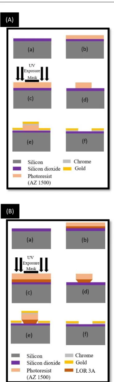
Figure 1. (A) Lift off process for gold metallization using single layer resist (B) Lift off process for gold metallization using bilayer resist; fabrication steps comprises of (a) silicon wafer
cleansing (b) spin coating of resist layer (c) UV exposure (d) development (e) metal evaporation using e-beam evaporator
(f) lift-off for patterning electrode
A. Lift Off Results
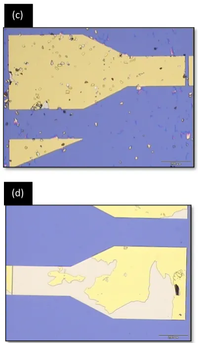
Figure 2 illustrates the results of lift off from various conditions. Figure 2 (a) demonstrates electrodes patterned from single layer resist profile. It can be clearly observed that retention has occurred at the channel area as the metal is not fully lift off. The retention in the sample remained strongly although it’s placed in an ultrasonic bath for
prolonged period of time. As reported in literatures, this is one of the most prevailing condition occurs in single layer resist profile. However, figure 2(b) demonstrates the well patterned electrodes structure from lift off process. Conditions for patterning these electrodes are optimal. It can be seen that the electrode structures are well pattern and gap in the channel area is clearly formed. This is due to implementation of bilayer resist profile and LOR as base coating.
Two stage development process in bilayer resist profile provides undercut which aids in complete lift off of metal without usage of ultrasonic bath. An undercut is the distance between leading edge of photoresist pattern and the edge of LOR structure (Wilson et al., 2015). In order to get undercut with negative slope, the bilayer resist was developed in two stage. In the first stage of developing process, the sample was developed for 20 seconds and post baked at 100℃ for 3 minutes. This is to ensure the photoresist is harden; prevent the overhang dropping off. At the second stage of development, the sample was developed at 20 seconds, 40 seconds, and 60 seconds respectively. Sample developed for 40 seconds gives perfect undercut with negative slope as illustrated in figure 3. This negative slope forms a discontinuous metal layer at the edges which are vital for penetration of lift off solution during lift off process. Our current work proved that electrode with 10 um gap size can be patterned with bilayer resist profile which gives desired undercut slope for ease lift off process. This work is compared with existing work as shown in Table 1.
However, figures 2 (c) and (d) shows the results of drawbacks and limitations faced in lift off process. Figure 2(c) shows the result of lift off process carried out in acetone for 30 minutes. It can be observed that the gold particles that has been lifted off drops back on top of the sample. This
is due to the insufficient amount of acetone in the beaker as it evaporates quickly in the air. Therefore, as lift off occurs the lifted particles drops back on the sample. Hence, amount of acetone or lift off solution needs to be taken into consideration for good lift off results. Moreover, figure 2 (d) shows the peeling of certain portion of gold materials from the substrate. This is due to the effects of ultrasonification. Lift off in ultrasonification need to be optimized by controlling the time taken and the way placing sample for ultrasonification. Placing for prolong period can leads to detachment of gold layer from its substrate.
Therefore, in order to pattern gold electrodes for the final step in photolithography which is lifting off process need to be optimized. Hence, implementation of bilayer resist profile provides well defined electrode structures. It is also worthy to take note that the acetone that being used for lift off process should have high purity for better output from lift off process.
Figure 2. (a) Pattern from optimized lift off technique (single layer resist profile) (b) Pattern from optimized lift off technique (bilayer resist profile) (c) Gold particles that have lift off falls back on sample (d) Gold detaches from
electrode during sonification
Figure 3. FESEM image of undercut image in bilayer resist profile
(a)
(d)
(b)
Table 1. Comparison on existing work on LOR as base layer for patterning electrode with 10 µm gap
Reference Type
of LOR developing First time
Second developing
time
Gap Size
Wilson et
al., 2015 10B 60 s
3.5 to 4.5 min
10 um
This work 3A 20 s 40 s um 10
B. Electrical Characterization
1. Two-point probe measurement
Two – point probe measurement was conducted to observe current –voltage relationship of the device fabricated. The linear line in the graph obtained (Figure 4) clearly demonstrates that the ohmic contact is achieved in between graphene layer and gold electrode as the work function of the both are close to each other. Therefore, it indicates that the contact resistance between electrodes and graphene is very small or negligible (Mao et al., 2013).
Figure 4. Two-point probe measurement to validate ohmic contactivity of GFET
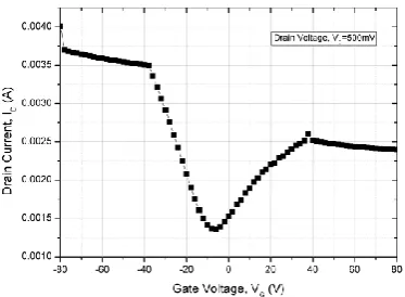
2. Three-point probe measurement
Three-point probe measurement was carried to define the operation of the GFET device fabricated. Back gate was formed using silver paste and I-V measurements were carried out to study the impact of gate voltage on the conductivity of GFET. Figure 5 illustrates the curve of drain current, Id as a function of gate voltage, Vg at minimum drain bias of 0.5 V. The curve demonstrates unique electronic ability of GFET where it
operates both in n-type and p-type conduction regions (Transistors et al., 2011). The charge neutrality point, commonly known as Dirac point occurs at Vg = - 4.0 V. The drain current, Id remains at a finite value of 0.00134 A at
VDirac = - 4.0 V. This clearly shows that the GFET
experienced minimum conductivity and highest resistivity at this point. Dirac point at – 4.0 V indicates that the graphene sheet behaves as p-type semiconductor and the channel is dominated by holes as majority charge carriers. Additional factors such as charges at the interface of graphene sheet, quality of substrate and graphene layer may attribute to the p-type ambipolar characteristics of GFET device (Selvarajan et al., 2017).
Figure 5.Transfer characteristics curve of GFET, Id vs Vg at Vd = 0.1 V
IV. CONCLUSION
prominient device to be used in GFET based biosensing applications.
V. ACKNOWLEDGEMENT
This research is supported by AKU-95 HICoE MEMS for Artificial Kidney grant funded by the Ministry of Higher Education (MOHE) Malaysia.
VI. REFEREENCES
Afsahi, S, Lerner, MB, Goldstein, JM, Lee, J, Tang, X., Bagarozzi, DA & Goldsmith, BR 2018, Novel graphene-based biosensor for early detection of Zika virus infection, Biosensors and Bio Electronics, vol. 100(August 2017), pp. 85–88.
Chaudhary, R, Sharma, A, Sinha, S, Yadav, J, Sharma, R, Mukhiya, R & Khanna, VK 2016. Fabrication and characterization of Al gate n-metal-oxide-semiconductor field-effect transistor, on-chip fabricated with silicon nitride ion-sensitive field-effect transistor, IET Computers and Digital Techniques, vol. 10, no. 5, pp. 268-272.
Chen, Y, Peng, K, & Cui, Z 2004, A lift-off process for high resolution patterns using PMMA/LOR resist stack,
Microelectronics Engineering, vol. 73–74, pp. 278–
281.
Fu, W, Feng, L, Panaitov, G, Kireev, D, Mayer, D, Offenhäusser, A, & Krause, HJ 2017, Biosensing near the neutrality point of graphene, Science Advances, vol 3, no. 10.
Han, SJ, Chen, Z, Bol, AA & Sun, Y 2011, ‘ Channel-length-dependent transport channel-length dependent transport behaviors of graphene field-effect transistors,
IEEE Electron Device Letters, vol. 32 , no. 6, pp. 812 –
814.
Golden, J., Miller, H., Nawrocki, D., & Ross, J. 2009. Optimization of bi-layer lift-off resist process, Proc. CS
MANTECH Conference, May 18th-21st, 2009, Tampa, Florida, US.
Hamzah, AA, Yunas, J, Majlis, BY, & Ahmad, I 2008, Sputtered encapsulation as wafer level packaging for isolatable MEMS devices: A technique demonstrated on a capacitive accelerometer,
Sensors, vol. 8, no. 11 pp. 7438–7452.
Haslam, C, Damiati, S, Whitley, T, Davey, P, Ifeachor, E, & Awan, S 2018, Label-free sensors based on graphene field-effect transistors for the detection of human chorionic gonadotropin cancer risk biomarker, Diagnostics, vol. 8, no. 1, pp. 5.
Marsi, N, Majlis, BY, & Hamzah, AA 2014, ‘The mechanical and electrical effects of mems capacitive pressure sensor based 3C-SiC for extreme temperature the mechanical and electrical effects of MEMS capacitive pressure sensor based 3C-SiC for extreme temperature, Journal of Engineering, vol. 2014.
Marsi, N, Majlis, BY, Mohd-Yasin, F & Hamzah, AA 2015, The fabrication of back etching 3C-SiC-on-Si diaphragm employing KOH + IPA in MEMS capacitive pressure sensor, Microsystem Technologies, vol. 21, no. 8, pp. 1651–1661. Mao, S, Yu, K, Chang, J, Steeber, DA, Ocola, L E, &
Chen, J 2013. Direct growth of vertically-oriented graphene for field-effect transistor biosensor,
Ordonez, RC, Hayashi, CK, Torres, CM, Melcher, JL, Kamin, N, Severa, G, & Garmire, D 2017, Rapid fabrication of graphene field-effect transistors with liquid-metal interconnects and electrolytic gate dielectric made of honey. Scientific Reports, vol. 7, no. 1, pp. 1–9.
Selvarajan, RS, Hamzah, AA & Majlis, BY 2017, Transfer characteristics of graphene based field effect transistor (GFET) for biosensing application, Biosensing and Nanomedicine X, vol. 10352.
Zheng, C, Huang, L, Zhang, H, Sun, Z, Zhang, Z & Zhang, G 2015, Fabrication of ultrasensitive field-effect transistor DNA biosensors by a directional transfer technique based ozn CVD-grown graphene, ACS Applied Materials and Interfaces, vol. 7, no. 31, pp. 16953-16959.
Liang, J, Kohsaka, F, Matsuo, T, Li, X, & Ueda, T 2008. Improved bi-layer lift-off process for MEMS applications. Microelectronic Engineering, vol 85, no. 5–6, pp. 1000–1003.
Mohamed. MA & Majlis, BY 2017, ‘Straightforward fabrication of low schottky barrier single-walled carbon nanotube transistors by direct growth method’ ,
Proceedings of 2017 IEEE Regional Symposium on Micro and Nanoelectronics (RSM), Batu Ferringhi, 2017, pp. 100-103.
Inami, N, Mohamed, MA, Shikoh, E & Akihiko 2008, Device characteristics of carbon nanotube transistor fabricated by direct growth method, Applied Physics Letters, vol. 92, no. 24, pp.243115.