RAHUL T. DAHATONDE, SHANKAR B. DEOSARKAR
Dept. of E & TC, Dr. Babasaheb Ambedkar Technological University, Lonere, 402 103, Tal. Mangaon, Dist. Raigad, INDIA.
http://www.dbatu.ac.in
Abstract
This paper discusses design and parametric evaluation of Rectangular Microstrip Antenna (RMSA) for GSM Communication. A simple RMSA is designed using transmission line model and analyzed using Method of Moment (MoM) based software IE3D for studying its behaviour with various parameters such as, its length, width, height of substrate, location of feed position, effect of substrate dielectric constant and effect of finite ground plane. It was observed that the theoretical results obtained using IE3D are in good agreement with measured results presented in literature.
Keywords – Rectangular Microstrip Antenna, parametric study.
1. Introduction
These days, MSAs are widely used in many applications due to their inherent advantages such as low profile, light weight, planer configuration and ease of fabrication. Therefore, there is lot of research going on in design and development of MSAs suitable for various communication engineering applications. In this paper, we have designed a simple RMSA using transmission line model. This RMSA is analyzed using Method of Moment (MoM) based software IE3D for studying its behaviour with various parameters such as, its length, width, height of substrate, location of feed position, effect of substrate dielectric constant and effect of finite ground plane.
2. Design of RMSA [1 – 2]
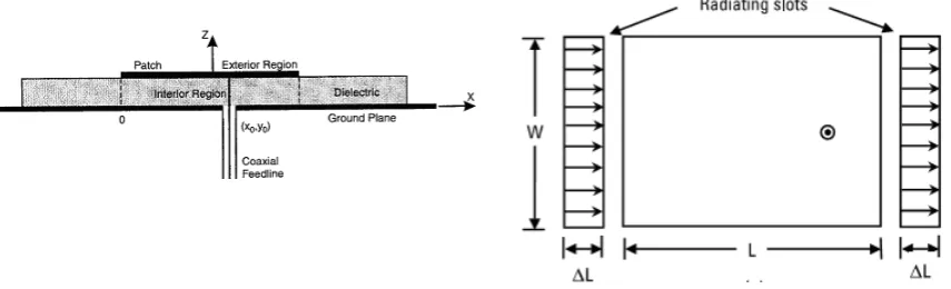
The basic RMSA is a strip conductor of dimensions L x W on a dielectric having dielectric constant r and thickness h backed by a ground plane. For RMSA width is comparable to wavelength to enhance radiation from edges. The substrate thickness is much smaller than the wavelength, therefore RMSA is considered to be 2D planar configuration for analysis.
Fields associated with MSA are divided into interior and exterior region as shown in Figure 1-a. Interior region is formed by the patch, portion of the ground plane under patch and walls formed by the projection of the patch periphery onto ground plane. Exterior region is formed by rest of the space which includes remainder of ground plane, remainder of dielectric, and top of the patch conducting surface [2]. The fields in the interior region can be modeled as a transmission line section. This gives rise to designation transmission line model (TLM). Fields in the exterior region comprise of radiation field, surface waves, and fringing field. The characteristic impedance Z0and the propagation constant j, for the line are determined by the patch size and substrate parameters. The periphery of the patch is described by four edges which are classified as radiating type or non-radiating type depending on the field variation along their length. Field variation along radiating edge is 2 and it’s constant along width (non-radiating edge) [1].
Figure 1-a. RMSA field distribution [2] Figure 1-b TLM representation of RMSA [1] The value of this effective dielectric constant is given by [1],
21 12 1 2 1 2 1 W h r r eff where, eff
is effective dielectric constant andr, h, W represent dielectric constant, height and width of the substrate, respectively.
For RMSA to be an efficient radiator, W should be taken equal to a half wavelength corresponding to the average of the two dielectric mediums (i.e., substrate and air) [1]
2 1
2 0
r f c W
For the fundamental TM10 mode, the length L should be slightly less than 2, whereis the wavelength in the dielectric medium. Here, 0 eff where 0is the free-space wavelength and eff is the effective dielectric
constant of the patch. From the voltage and current distribution shown in Figure 2-a it is clear that, voltage is maximum and current is minimum along the width of the patch due to the open ends. Therefore, the input impedance of the RMSA varies from zero value at its center to the maximum value (180-Ω) at its radiating edges.
Electromagnetic field lines at the edges as shown in Figure 2-b can be resolved into normal and tangential components with respect to ground plane.
Figure 2-a. Voltage and Current distribution Figure 2-b E-field distribution
The normal components of E-field at the two edges along the width are in opposite directions and thus out of phase since the patch is 2long and hence they cancel each other in broadside direction.
The tangential components are in phase; hence the resulting fields combine to give maximum radiated field normal to the surface of the structure. Hence edges along the width can be represented as two radiating slots,
2
equation.
From these equations, a RMSA was designed to operate over GSM frequency of 1.8 GHz. The optimized length and width of the RMSA was found to be 39 mm and 51 mm, respectively. This RMSA was simulated using Zeland’s MoM based EM Simulation Package, IE3D [3]. For simulations, the FR4 substrate with dielectric constant of 4.47 with thickness of 1.59 mm was considered.
3. Parametric Study of RMSA
The RMSA designed in earlier section was analyzed using software IE3D for studying its behaviour with respect to various parameters such as feed point location, width and length of the patch, height, loss tangent and dielectric constant of the substrate, diameter of feeding probe and size of ground plane.
3.1 Effect of feed-point location
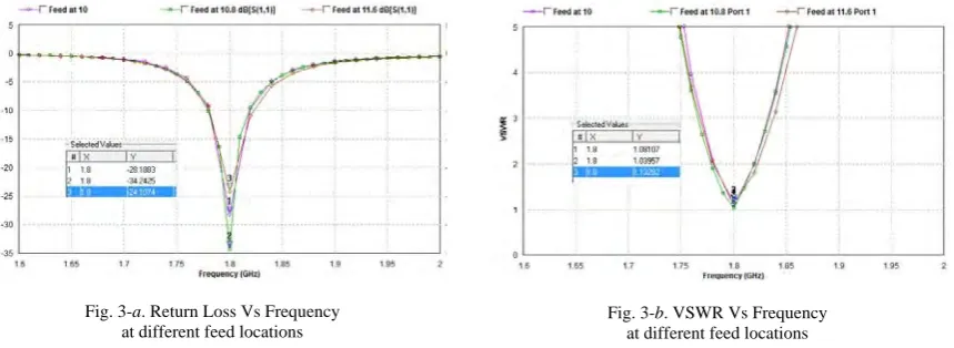
As discussed above, the input impedance of the RMSA varies from zero value at its center to the maximum value (180-Ω) at its radiating edges. The feed-point should be located on the patch at a point where input impedance is 50-Ω at resonance frequency. The center of the patch is taken at origin and feed-point location is given by coordinates (Xf, Yf) with respect to origin. There exists a point along the length of the patch, where RL is minimum [4]. In order to locate optimum location of feed point, return loss is calculated using IE3D at different locations on the patch and a point where RL is most negative is selected as a feed-point. Figure 3-a, -b show the curves obtained for return loss and VSWR Vs frequency at different feed locations. It is seen that the minimum value of RL, -34.24 dB, occurs at feed location (10.8, 0). VSWR at this point is 1.03. Therefore, this is considered as optimum feed point location.
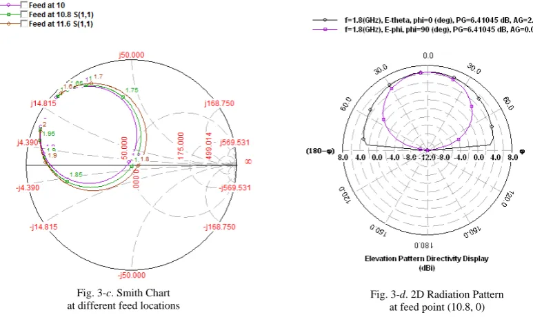
Figure 3-c shows Smith Chart obtained at different feed locations. It is seen that as Xf increases from 10 mm to 11.6 mm (i.e., the feed point is shifted toward the edge of the patch), the input impedance loci shifts in the right direction on the Smith chart implying that the impedance is increasing. It can be remembered that impedance at the center of the patch is 0 Ω and at edges it is 180 Ω. The 2D radiation pattern of RMSA obtained at feed location of (10.8, 0) shows that HPBW in E- and H-plane is 105 and 76 degrees respectively and directivity is 6.4 dB.
Thus it is clear that feed location (10.8, 0) is the optimum feed location for this RMSA at 1.8 GHz. Its various performance parameters are summarized in following table:
Feed location Return loss VSWR Directivity Bandwidth Input Impedance Fig. 3-a. Return Loss Vs Frequency
at different feed locations
3.2 Effect of patch width
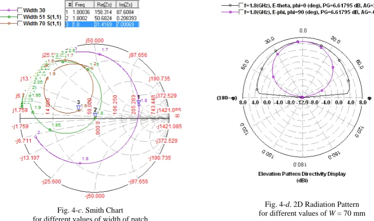
To study the effects of change in width of patch on its performance, its width varied from 30 mm to 70 mm, keeping the feed-point location same for all simulations at (10.8, 0) with respect to origin. It is observed that width of the patch has significant effect on BW, gain and input impedance of the RMSA.
Figure 4-a and –b shows the curves for return loss and VSWR Vs frequency, for different values of width of patch. From Figure 4-a, it is seen that, BW increases with increase in width of patch, however, RL decreases. The minimum value of RL, – 34.24 dB, occurs only for designed width of 51 mm, indicating perfect match of MSA with feed line.
Also resonance frequency decreases from 1.84 GHz to 1.79 GHz, with increase in W from 30 mm to 70 mm, because width is inversely proportional to resonance frequency. Similarly, from Figure 5-b, it is seen that VSWR at resonance frequency of 1.8 GHz is 1 only for designed width of 51 mm. However, effects of change in width of the patch on performance of MSA can be studied better, if feed-point is optimized for each design. Also, with increase in width of patch, the radiation from the radiating edges increase, therefore the radiation resistance decreases resulting in decrease in input impedance. This is apparent from the Smith Chart shown in Figure 4-c, for different values of width of patch.
Aperture area of MSA increases with increase in width, causing gain to increase, since gain is directly proportional to aperture area. For W=70 mm, directivity is 6.62 dB, which is slightly better than directivity at designed width of 51 mm. The HPBW in H-plane decreases but in E-plane is almost constant since beamwidth increases in H-plane.
Fig. 3-c. Smith Chart at different feed locations
Fig. 3-d. 2D Radiation Pattern at feed point (10.8, 0)
Fig. 4-a. Return Loss Vs Frequency for different values of width of patch
Thus with increase in width of patch, BW, directivity and gain increase, however, resonance frequency and input impedance decrease.
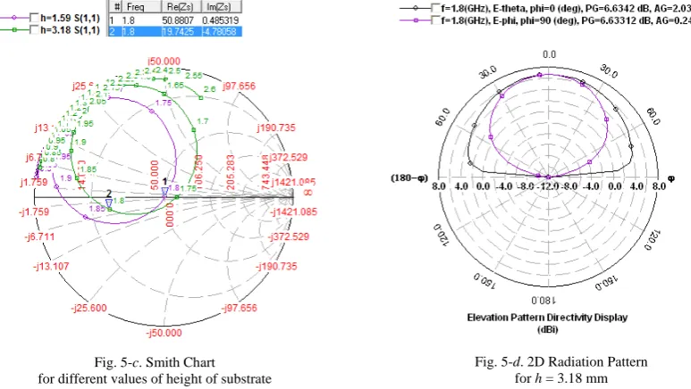
3.3 Effect of height of substrate
A substrate in MSA is principally required for the mechanical support of the antenna metallization. A thicker substrate besides being mechanically strong, will increase the radiated power, reduce conductor loss and improve impedance BW. However, it will also increase weight, dielectric loss, surface wave loss, and extraneous radiations from the probe feed. These effects are similar to decrease in substrate dielectric constant [2]. Resonance frequency, BW, gain and input impedance of RMSA were studied for increase in h.
From the RL Vs frequency curve in Figure 5-a, it’s seen that, with increase in h from 1.59 mm to 3.18 mm resonance frequency decreases from 1.8 GHz to 1.76 GHz. Because, with increase in h, the fringing fields from the edges increase. This increases the extension in length ∆L and hence the effective length, thereby decreasing the resonance frequency. Also, resonance freq reduces from 1.8 GHz to 1.76 GHz and BW increases to 62MHz, with increase in h.
Smith Chart shown in Figure 5-c, shows that with increase in h, input impedance curve moves clockwise (i.e., an inductive shift occurs), because coaxial feed probe length increases, increasing inductance. On the other hand with the increase in h, the W/h ratio reduces which decreases effective dielectric constant and hence increases the resonance frequency. However, the effect of the increase in ∆L is dominant over the decrease in effective dielectric constant. The 2 D radiation pattern in Figure 5-d, shows that the directivity of the antenna increases marginally to 6.6 dB, because the effective aperture area is increased slightly due to increase in ∆L.
Fig. 4-c. Smith Chart for different values of width of patch
Fig. 4-d. 2D Radiation Pattern for different values of W = 70 mm
Fig. 5-a. Return Loss Vs Frequency for different values of height of substrate
Thus with increase in height of substrate, BW and directivity of MSA increases but resonance frequency decreases. However, input impedance becomes more inductive.
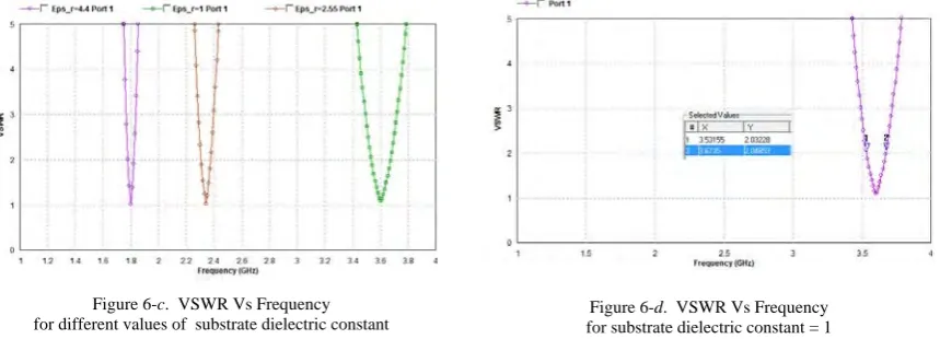
3.4 Effect of substrate dielectric constant
A low value of r will increase the fringing field at the patch periphery and thus the radiated power. An increase in h has similar effects on antenna characteristics as decrease inr[2]. Thus increase in h or decrease in rwill increase the radiated power, reduce conductor loss and improve impedance BW. VSWR, input impedance and return loss characteristics were studied for three different values ofr.
From RL Vs frequency curve shown in Figure 6-a, it is seen that when ris decreased from 4.4 to 1, the resonance frequency increases from 1.8 GHz to 3.6 GHz.
Fig. 5-c. Smith Chart for different values of height of substrate
Fig. 5-d. 2D Radiation Pattern for h = 3.18 mm
Figure 6-a. Return Loss Vs Frequency for different values of substrate dielectric constant
Figure 6-b. Smith Chart
Thus with decrease inr, BW and resonance frequency increase and input impedance becomes more inductive.
3.5 Effect of probe diameter
An RMSA can be fed with different types of connectors, such as SMA, TNC, and N type, depending upon the application. The diameters of these connectors are different. Input impedance and VSWR plots for two different connectors, with d = 1.2 mm and 4 mm are observed.
As the probe diameter increases, the probe inductance decreases for the same substrate thickness. With an increase in the probe diameter, the resonance frequency increases slightly (Figure 7-a) and the probe inductance decreases causing the impedance plot to move in the anticlockwise direction (Figure 7-b).
3.6 Effect of finite ground plane
For all the simulations and measurements discussed in earlier sections, we have considered RMSA with infinite ground plane, because the transmission line model is based on assumption of infinite ground plane [1]. However, in practice, MSAs are designed and fabricated with ground plane of sufficiently larger size but still this is not infinite. It is proved in [1] that when the size of the ground plane is greater than the patch dimensions by approximately six times the substrate thickness all around the periphery, the results are similar to that of the infinite ground plane. Thus for this RMSA, the length and width of finite ground plane are calculated as, 47.76 mm and 60.22 mm, respectively.
From RL and VSWR curves in Figure 8-a and -b, respectively, it is observed that the resonance frequency of the RMSA for finite and infinite ground plane is almost the same.
Figure 6-c. VSWR Vs Frequency for different values of substrate dielectric constant
Figure 6-d. VSWR Vs Frequency for substrate dielectric constant = 1
Figure 7-a. Return Loss Vs Frequency
However input impedance with finite ground plane is slightly higher than with infinite ground plane (Figure 9-c). The 2-D radiation pattern shown in Figure 9-d, indicates that there are back lobes present with finite ground plane, whereas there are no back lobes with infinite ground plane. Therefore, directivity with finite ground plane is less.
It was observed that software IE3D assumes infinite ground plane by default since it’s based on Method of Moment (MoM) which considers only infinite ground plane. Therefore, during simulations, with infinite ground plane, software performs meshing only on radiating patch and simulates it. Therefore, the simulation time for RMSA with infinite ground plane is small compared to RMSA with finite ground plane.
3.7 Effect of loss tangent
Substrates having a low dielectric loss are expensive. For initial testing or for designing new MSA configurations, sometimes low-cost substrates are used, but generally these have larger tan value [1]. Hence, it is important to know the effect of tan on the performance of the antenna. VSWR and input impedance of the designed RMSA was studied for three different values of tan (0.0001, 0.01 and 0.02).
From RL and VSWR Vs frequency curves in Figure 9-a and –b, show that with an increase in tan from 0.0001 to 0.02, the resonance frequency remains almost the same. In Figure 10-b, for tan = 0.0001 there is no point corresponding to VSWR≤2, therefore BW appears almost zero. However, with an increase in tan, the losses in the patch increase leading to an increase in BW, which is around 50 MHz for tan = 0.02. Due to increase in loss tangent, the losses in the dielectric material increase therefore input impedance decreases, shifting the impedance plot toward the left side Figure 9-c.
Fig. 8-a. Return Loss Vs Frequency
with finite and infinite ground plane Fig. 8-b. VSWR Vs Frequency with finite and infinite ground plane
Figure 8-c. Smith Chart with finite and infinite ground plane
However, 2 D radiation pattern and hence directivity for different values of tan remains almost the same. Thus with an increase in tan, BW increases, input impedance decreases and directivity remains the same.
3.8 Effect of dielectric cover
MSAs are sometimes covered with a dielectric layer to protect them from the environment, or painted with dielectric material. The dielectric layer influences the characteristics of the antenna and, in general, reduces the resonance frequency due to increase in the effective dielectric constant [5]. Effect of dielectric cover with
r
=4.4, on VSWR, return loss and input impedance of patch was studied for different values of height of superstrate, i.e. h1 = (0, 1.59, 3.18, 4.77).
Figure 9-a. Return Loss Vs Frequency for different values of tan
Figure 9-b. VSWR Vs Frequency for different values of tan
Figure 9-c. Smith Chart for different values of tan
As seen from the RL and VSWR plots shown Figure 10-a and –b, with increase in superstrate thickness from 0 mm to 4.77 mm, the resonance freq decreases from 1.8 GHz to 1.71 GHz. Also increase in superstrate thickness implies that the loss in the dielectric material and hence input impedance decreases, so the impedance plot shifts toward the left side.
Conclusion
In order to study performance of RMSA with change in various parameters such as, its length, width, height of substrate, location of feed position, effect of substrate dielectric constant and effect of finite ground plane, an RMSA was designed using transmission line model and analyzed using Method of Moment (MoM) based software IE3D. It was observed that the theoretical results obtained using IE3D are in good agreement with measured results presented in literature.
References
[1] Kumar G. and Ray K.P., Broadband Microstrip Antenna, Artech House, London, 2003.
[2] Garg, I. Bahl, A. Ittipiboon, and P. Bhartia, Microstrip Antenna Design Handbook, Artech House, London, 1980. [3] IE3D 12.0, Zeland Software Inc., Fremont, CA, USA, 2008.
[4] C. Balanis, Antenna Theory Analysis & Design, John Wiley & Sons, 2nd Ed., 1997.
[5] I. J. Bahl, et.al., “Design of Microstrip Antennas Covered with Dielectric Layer”, IEEE Trans. Antenna Propagation, Vol. 30, 1982, pp. 314-318.
[6] Bhartia P., Millimeter-Wave Microstrip and Printed Circuit Antennas, Artech House, London.
Author Biography
Rahul T. Dahatonde, received his B. E. and M. Tech. degrees in Electronics & Telecom. Engineering in the year 2001 and 2003 from North Maharashtra University, Jalgaon and Dr. B. A. Technological University, Lonere, respectively. He is currently pursuing his Ph.D. from Dr. B.A.T.U., Lonere in the area of Microstrip Patch Antennas. His research interests include antennas, microwaves and EMI/EMC.
He has published around 10 research papers in various international and national journals/conferences. He is life member of ISTE, India.
Dr. Shankar B. Deosarkar received M.Tech. and Doctorate Degree in the area of Microwave Communication in the year 1990 and 2004, respectively from S.G.G.S. Institute of Engineering and Technology, Nanded. Currently, he is a Professor of Electronics & Telecommunication Engineering at Dr. B. A. Technological University, Lonere. He is having around 21 years of experience in academics. He has about 50 research publications to his credit at the National and International level.