134
Design Of EMI Filter For Flash Lamp Power
Supply
Amrita Bhatt, Sunil Shah, Dr. M. S. Ansari
Abstract: Conducted and radiated electromagnetic interference in embedded and VLSI systems have become important in recent years with increase in clock frequency and reduction in physical dimensions of interconnects. It is important to understand the noise components in terms of current paths and the mitigation techniques. Although the common mode and differential mode components of conducted noise are analyzed in the context of a power electronics system, the analytical and theoretical techniques hold good for other domains as well such as embedded systems and VLSI. This paper deals with modelling, design, and development of an EMI filter for conducted mode noise in flash lamp power supply. Also, a design procedure of EMI filters sustaining to the military standard 461E is presented and it is based on practical measurement of conducted emissions. Design procedure in this paper considers common mode and differential mode separately. The paper also consists of considerations for magnetic core material, integrated common mode (CM), common mode choke size optimization, and differential mode (DM) choke etc. Design examples are given and are experimentally verified.
Index Terms: Common mode (CM), Differential mode (DM), Electromagnetic Interference (EMI), Equipment under Test (EUT), Line Impedance Stabilization Network (LISN).
————————————————————
1
INTRODUCTION
Electromagnetic interference (EMI) can be generated by any electrical or electronics devices or anything that uses
controls or produces electrical energy. When
electromagnetic energy enters where it is not required, it can interfere with device’s operation or use. It is therefore important to manage the production of electromagnetic noise in the product and the system design. If noise sources are not taken into account during initial design stage, it can result in expensive and time-consuming fixes. Electromagnetic interferences for instance are the major issue in flash lamp power supply [1-3]. In this paper, describes a design procedure of EMI filters for flash lamp power supply. This procedure is based on examination of conducted EMI problems and use of different EMI diagnostic tools. Current probes can be used to measure both common mode (CM) noise, differential mode (DM) noise, and conducted ode noise which makes the filter design process much easier [4]. In this paper, review of
conducted EMI problems, factors affecting EMI
performance and issues of filter design is discussed. A practical approach of designing EMI filter is described. Filter design was simulated with the help of PSPICE. Numerical examples will be given and are experimentally verified.
2 EMI ANALYSES
Origin and path of CM and DM are discussed. Switching of large voltage or current generates electromagnetic interference in different frequency range. In general emission below 30 MHz is transferred to other devices through conduction mode. Beyond 30 MHz the EMI transmission is through radiation. Conducted emission is divided into common mode and differential mode.
2.1 Components of Conducted EMI Noise
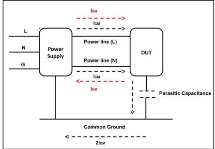
Conducted EMI noise is characterized as common-mode (CM) and differential-mode (DM) noise. CM noise is defined
as noise generated due to common mode current ICM on
line (L) and neutral (N). It returns through ground conductor wire. Common mode current flows in same direction from L and N and is coupled through parasitic capacitance to ground conductor wire. Total common mode current
through ground conductor is 2ICM whereas, DM noise is
generated due to differential mode current ( ).
Figure 2.1 Conducted Electromagnetic Interference
It follows from line (L) and returns back through neutral (N) conductor wire. Differential mode current propagates in opposite direction on L and N as shown in Fig. 2.1.
2.2 Measurement of Conducted EMI
Conducted mode noise is estimated by measuring noise current across a stabilized impedance of 50 Ω. Conducted emission regulated by FCC lies in the range of 450 kHz-30 MHz whereas for CISPR 22 this range is from 150 kHz- 30 MHz. When testing a device, for compatibility with FCC and CISPR 22 limits, a LISN is placed between device under test and power output. Due to difference in frequency ranges of FCC and CISPR regulations, LISN have similar layouts but different component values [6-7]. Figure 2.2 shows test setup for compliance test of conducted _________________________________
135
emission. As shown in the figure 2.2, ac powers to device under test are fed through LISN. Ports are available in LISN which is monitored by spectrum analyzer/DSO to estimate conducted noise on AC phases. Since the output current from device under test depends on load on AC power line, and this load is the impedance seen from the device looking into the AC power output. This certainly changes over the measurement frequency range from output-output. It is inadequate to measure noise currents on power line with current probe. The device under test is connected to LISN as mentioned earlier, the first purpose of LISN is to stabilize device under test. Second purpose is to block external noise that exit’s on the power supply line entering the device’s power line. Any noise currents from the power supply line that enters the device’s ac power line will add to conducted emission from device. It is important that the LISN prevents noise entering from power supply line to the device’s power line. LISN must satisfy objectives over entire frequency range of conducted emissions 450 kHz to 30 MHz for FCC regulations and 150 kHz to 30 MHz for CISPR 22 regulations.
Figure 2.2 Test setup for Conducted EMI measurement
2.3 EMI Standards
There are several standards for different types of applications in EMI analysis. These standards differ by their frequency range or amplitude of noise and whether the type of noise measured is in form of voltage or current. They have their own noise measurement experimental setup, and LISN circuits. Most common EMI standards begin at 150 kHz and end in megahertz range about 30 MHz, like DO160D standard [8]. However military standard 461E [9] starts at 10 kHz and end at 10 MHz. Government bodies have instituted standards which set specific limits on the quantities of radiated and conducted noise emissions in order to sell a product within a country. Federal Communications Commission and Department of Defense are regulatory bodies in United States whereas; European Economic Consortium (EEC) standards are set by the Europe. There also exists an international body known as International Special Committee on Radio Interference (CISPR) and a committee of the International Electron technical Commission (IEC), which sets standards that, is then adopted by individual nations to facilitate international trade.
3 PRACTICAL APPROACH OF DESIGNING
EMI FILTER
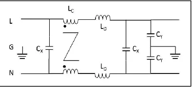
There are several types of filters, for example, passive EMI filter, active EMI filter and hybrid EMI filter. However, the passive EMI filter is simpler than others. A typical procedure used in [4, 5] is considered to design power line EMI filter. A basic network topology is used, C-L-C for DM filter and L-C for CM filter to attenuate both CM and DM noise. From figure 5.7 it is noted that some elements of filter affect either CM or DM noise and some affect both CM and DM noise.
The capacitors affect DM noise whereas;
capacitors attenuate both CM and DM noise.
The main component of the filter is common mode choke ( ) which attenuates only CM noise but
leakage inductance ( ) between two windings of
affect DM noise only. It could be helpful in some cases an additional inductor in series with the choke to increase the total DM inductance if the leakage produced by CM choke is too small [10].
Figure 3.1 Passive EMI Filter equivalent circuit
Equivalent circuit of the filter for CM and DM mode is represented in figure 6.3 and figure 6.4 respectively.
Network topology for CM filter is L-C type with
capacitors connected in parallel [1]. And, similarly for DM filter topology used is C-L-C or π type where two capacitors are used [1]. Main point to be noted is that the LISN is characterized for each line is, by connecting 50 Ω resistors and it is approximated by a 25 Ω for CM and 100 Ω for DM, by using two resistors in parallel or in series. After the circuit of filter is selected, component values are determined. Y- Capacitors are easily determined from the leakage current limit [4], which is given in the safety standards applicable to DUT. Simple calculations of
inductors and capacitors are needed. The is cut-off
frequency of common mode filter. and are total
common mode inductors and capacitors in EMI filter.
Common mode Inductance is presented by [5];
(3.1)
And is presented by . Since are in
parallel. dominates , so equation of common mode
path is expressed as;
√
(3.2)
√[ ]
136
Similarly, for differential mode noise is the cut-off
frequency of differential mode filter. and are
differential mode inductor and capacitor in EMI filter. In
equation (3.4) is represented by [ ] and
is represented by . is the leakage
inductance of common mode choke. Final equation of differential mode path is;
√
(3.4)
√
(3.5)
3.1 Design Flow
Based on preceding discussion, a flow chart for EMI filter is presented in figure 3.1. Block I is to determine CM and DM filter cut-off frequency. Based on the information provided in block I, component values of both CM and DM filter is determined separately. After deriving component values, is the assembling of both filters. The filter design obtained should meet both high frequency and low frequency specifications. However, high-frequency effects are difficult
to deal at the design stage of filter, and maycause violation
of high-frequency design specification. High-frequency effects include parasitic capacitance effect of inductor, permeability reduction of choke core, and parasitic inductance effect of filter capacitors. These effects are difficult to be predicted without experiments.
Figure 3.2 Flow chart for design of EMI filter
4 DESIGN PROCEDURE FOR EMI FILTER
Based on the discussion in above section, a procedure for
filter design is presented. Acommonly used filter topology
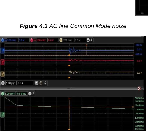
shown in Figure 3.2 is used to illustrate. Main objective of the procedure is to meet the high frequency specification. Once designed and built, modification can be made according to frequency range of noise. Above figure 4.1 shows the circuit diagram of Flash lamp power supply which is divided into two parts Trigger circuit and Capacitor bank circuit whereas, figure 4.2 shows the total conducted mode noise generated in flash lamp power supply, measured without EMI filter with the help of DSO/Spectrum Analyzer. Whereas, figure 4.3 and 4.4 shows the AC line ommon mode noise and AC line differential mode noise.
Figure 4.1 Circuit diagram of Flash lamp Power Supply
Figure 4.2 Conducted mode noise of flash lamp power supply without EMI filter
Determine CM & DM filter corner frequency
Design Common Mode choke
(Lcm) Mode Inductance (Ldm)Calculate Differential
Calculate value of Y capacitors
Calculate value of X capacitors
Assemble filter components
Assemble filter components
CM Filter DM Filter
Assemble CM & DM Filter
Test the complete filter
If specifications meet?
End YES
137 Figure 4.3 AC line Common Mode noise
Figure 4.4 AC line Differential Mode noise
4.1 DESIGN EXAMPLE
A design example is given below to illustrate the design steps described above. Filter topology shown in Figure 3.1 is used. One example is for the flash lamp power supply. The result of example is verified experimentally.
Step I- From Figure 4.3 and 4.4, = 900 kHz and
= 100 kHz
Step II a): Calculate CY according to equation (3.3)
[
( )]
Select and the leakage inductance
are obtained by measurement.
Step 4b): Using in (2), there are infinite
sets of solution for LDM and CDM. In this case an additional
inductor in series with the CM choke is placed to increase the total DM inductance if the leakage produced by CM
choke is too small [10]. and are differential mode
inductor and capacitor in EMI filter. In equation (3.5) is
represented by [ ] and is represented by
. is the leakage inductance of common
mode choke. Where, and
which makes ,
[ ( )]
X capacitors ( ) of value 63 nF each, .
Figure 4.5 (a) EMI filter ckt. For design example
Figure 4.5(b) Noise spectrum at 100 kHz without filter
Figure 4.5 (c) Noise spectrums at 100 kHz DM noise with EMI filter
Figure 4.5 (b) and 4.5 (c) is the noise spectrum graph for differential mode noise at 100 kHz.
138 Figure 4.5 (e) Noise spectrums at 900 kHz CM noise with
EMI filter
Figure 4.5 (d) and 4.5 (e) is the noise spectrum graph for common mode noise at 900 kHz.
Figure 4.5 (f) AC line Conducted Mode noise with EMI filter using DSO
Figure 4.5 (f) shows the graph plot for conducted mode noise with EMI filter and is displayed using digital
oscilloscope.
5 CONCLUSIONS
A practical procedure for EMI filter design is presented. This procedure leads to quick filter design which meets the high-frequency part of design specifications. This procedure facilitates the EMI filter design process and reduces cut-and-trial effort. A typical filter design methodology is used for the illustration in paper and procedure has been experimentally verified in flash lamp power supply applications. The same procedure can be extended to other filter topologies like m-derived filters, but it requires further work.
REFERENCES
[1] Richard Lee Ozenbaugh, Marcel Dekker Inc. “EMI filter
design”.
[2] P. V. Y. Jayasree, “Design of Active Electromagnetic
Interference Filter to Eliminate Common-mode Noise in Conducted Interference” April 2012.
[3] Shashwatee Paul, Sri. S. SrinivasaRao, “Power Line
Filter Design using equivalent circuit of passive lumped components”, 2014.
[4] Shih, Fu-Yuan; Yie-Tone Chen; Yan-Pei Wu; Yie-Tone
Chen, "A Procedure for Designing EMI Filters for AC
Line Applications," Power Electronics, IEEE
Transactions on , vol.11, no.1, pp.170,181, Jan 1996.
[5] J. Jiraprasertwong, and C. Jettanasen, “Practical
design of passive EMI filter for reduction of EMI
generation” Proceedings of the International
MultiConference of Engineers and Computer Scientists 2015 Vol II, IMECS 2015, March 18 - 20, 2015, Hong Kong.
[6] Pande D.C. “EMC measurements as per military
standards”, Electron & Radar Dev. Establ., Bangalore, India 1997.
[7] Kodali. W, “EMC Standards”, 2001.
[8] RTCA, Inc., “Environmental Condition and Test
Procedure for Airborne Equipment” in DO 160D, Dec 2004.
[9] Department of Defense, “Requirements for Control of
Electromagnetic Interference Characteristics of
Subsystems and Equipment” in Military Standard461E, Aug 1999.
[10]Yoann Y. Maillet, “High-Density Discrete Passive EMI