MULTIRATE DSP AND ITS TECHNIQUE FOR LOW POWER HIGH
SPEED VLSI OF INTERPOLATOR UNIT
Rajendra M. Rewatkar*Dr. Sanjay L. Badjate**
ABSTRACT
Paper Presents Multirate DSP and its techniques of the system which includes sampling rate
conversion. This technique is necessary for systems with different input and output sampling rates,
as the proposed multirate device is Interpolator; In order to build interpolator FIR filter with
upsampler: Shift register, D F/F and Multiplexer circuits are design and Simulation done on
Active HDL and ALTERA QUARTUS–II platform. The circuit obtained is verified and
implemented successfully. Then it is synthesized using 45 nm library in synopsis tool with
constraint of low power and area. The circuit uses device level and circuit level optimization to
obtain a very low power. Reduction of power consumption is important for VLSI system and also it
becomes one of the most critical design parameter. There are many reasons to change the sample
rate of a sampled data signal. Here, author discuss the two basic operations in a multirate system
i.e. decimation and interpolator. Also the use of multirate filters at the interfaces of continuous &
sampled data which results in a cost reduction components as well as improvement of signal
quality. The proposed approach achieves comparable reductions because of a hybrid allocation
scheme and multiple optimization iterations. The usefulness of the proposed system for low power
design of FIR filters in interpolator is shown
Keywords: VLSI-Very large scale integrated circuit, PCS -Personal communication services-,
Active HDL-Hardware description language, RTL-Register transfer logic, DSP-Digital signal
processing, VHDL-Very high speed hardware description language
I.INTRODUCTION
In single-rate systems, only one sampling rate is used throughout a digital signal processing systems, whereas in multirate systems the sampling rate is changed at least once. Multirate systems have gained popularity since the early 1980s and they are commonly used for audio and video processing,
Communication systems, and transform analysis, there are many reasons to change the sample rate of a sampled data signal. Applications include conversion of variable rate input data to fixed rate output data in a modulator and the inverse task of converting fixed rate input data to variable rate output data in a demodulator. Another application involves sample rate changes so that filtering can be performed at the Nyquiest rate of the signal being processed. In one major application, the multirate filter is used to increase the sample rate of a sampled data signal prior to its delivery for processing by the digital to analog converter involved in transferring the signal between the sampled data world and the continuous world. In the other major application, the multirate filter is used to decrease the sample rate of a sampled data signal after being formed at the output of an analog to digital converter so that filtering can be performed at the Nyquist rate of the signal being processed. [8]. In the other major application, the multirate filter is used to decrease the sample rate of a sampled data signal after being formed at the output
of an analog to digital converter. But due to the limited power-supply capability of current battery
technology, PCS devices needed low-power VLSI design to minimize the total power consumption, while maintaining the system performance [1]. In general, the direct implementation of the system has a constraint that the speed of the processing elements must greater than input data rate. It cannot compensate the speed penalty under low supply voltage. Therefore, the processing elements can be operated at a lower supply voltage to reduce the power dissipation and the data throughput rate is not degraded. Basic operations of multirate processing are Upsampler, Downsampler, Decimation and Interpolation.
Fig.1 Block-diagram representation
B.Downsampling:
A down-sampler with a down-sampling factor M, where M is a positive integer[3], develops an output sequence y[n] with a sampling rate that is (1/M)th of that of the input sequence x[n]. If the original sequence contains frequency components above π / M, the downsampler should be preceded by a low-pass filter with cutoff frequency π / M.
Fig.2Block diagram representation
C.Decimation: -Decimation is a technique for reducing the number of samples in a discrete-time signal [3]. The
element which implement this technique is referred to as a decimator.
D.Interpolation: Interpolation is the exact opposite of decimation. It is an information preserving operation, in that all samples of x[n] are present in the expanded signal y[n]. The mathematical definition of L-fold interpolation is defined by Equation 2 and the block diagram notation is depicted in Figure 4. Interpolation works by inserting (L–1) zero-valued samples for each input sample. The sampling rate therefore increases from Fs to LFs.Expansion process is followed by a unique digital low-pass filter called an anti-imaging filter. Although the expansion process does not cause aliasing in the interpolated signal, it does however yield undesirable replicas in the signal’s frequency spectrum. In Figure 3 below, it depicts 3-fold interpolation of the signal x[n] i.e.
II.MULTIRATE DESIGN METHODOLOGY
Since, the data rate in the multirate implementation is M-times slower than the original data rate while this feature to either the low-power implementation, or the speed-up of the DSP systems. This design methodology provides a systematic way to design low-power DSP systems at the architectural level. The multirate implementation provides a direct and efficient way to compensate the speed penalty in low-power designs at the architectural level.
Authors design the interpolator procedure can be extended for an arbitrary M.
III.RESULT
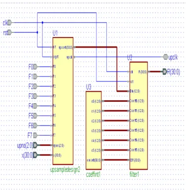
Implementation of the interpolator by using active HDL Quartus-II shown as follows
Simulation of Interpolator:
Simulation and Synthesis of Interpolator:
Then, it is synthesized using 45 nm library in synopsis tool with constraint of low power and area. The following report for power and area is obtained. Also, we obtained design vision schematic and encounter layout for interpolator as shown in figure 7 and figure 8.
Interpolator Area/Power Report
****************************************
Report: Area
Design: Interpolator_1
Version: B-2008.09
Date : Wed Apr 10 17:41:44 2013
**************************************** Library(s) Used:
gscl45nm (File: /home/raj/libfortech/45n/gscl45nm.db) Number of ports: 76
Number of nets: 1226 Number of cells: 155 Number of references: 52
Combinational area: 16781.698437 Noncombinational area: 825.968018
Net Interconnect area: undefined (No wire load specified) Total cell area: 17607.666454
Total area: undefined
Loading db file '/home/raj/libfortech/45n/gscl45nm.db'
Information: Propagating switching activity (low effort zero delay simulation). (PWR-6) ****************************************
Report: Power
-analysis effort low
Design: Interpolator_1
Version: B-2008.09
Date : Wed Apr 10 17:41:51 2013
****************************************
Power-specific unit information: Voltage Units = 1V
Capacitance Units = 1.000000pf Time Units = 1ns
Dynamic Power Units = 1mW (derived from V, C, T units) Leakage Power Units = 1nW
Cell Internal Power =139.4195 uW (81%) Net Switching Power = 33.0861uW (19%) Total Dynamic Power =172.5056 uW (100%) Cell Leakage Power =95.8968uW
IV.CONCLUSION
The low power and area constrain is verified for the implementation of module of interpolator after optimization with multirate signal processing approach is presented. Authors have used Active-HDL for simulation of design using Quartus –II platform. Authors have used synopsis tool of 45 nm library to design vision and the encounter layout. Also, design the model of interpolator with top level system design approach and low-power methodology and area for system. The results are found satisfactory. Also, the result of design of interpolator using optimization at device level and circuit level by factor M found satisfactory. Physical testing verified that implementation worked correctly for all factors. The low power design using multirate approach reduces the power consumption to a great extent. The proposed methodology provides a systematic way to derive low power and low area system.
REFERENCES
[1]An- Yeu Wut I, J. Ray Liu, Zhongying Zhang, Kazuo Nakajim, Arun Raghupathy “Low-Power Design Methodology for DSP Systems Using Multirate Approach”.
[2]Shyh-JyeJou, Shou-Yang Wu and Chorng-Kuang Wang “Low- Power Multirate IF Digital Frequency Down Converter”.
[5]P. Schaumont, S. Vernalde, M. Engels and I. Bolsens “Digital Upconversion Architecture for Quadrature Modulators”
[6]Sayfe Kiaei “Systematic Derivation of VLSI Arrays for Digital DSP Algorithms”.
[7] Dr. K.B. Khanchandani, Kundan Kumar “Design and Implementation of Custom Low Power DSP blocks for Biomedical Applications”.
[8]’ Multirate DSP and its technique to reduce the cost of the analog signal conditioning filters’ publish in IJCA-Aug 2010 by Richa Maheshwari Manisha Bharadia Meenakshi Gupta